
Summary of Contents for MeiGLnk SLM756P
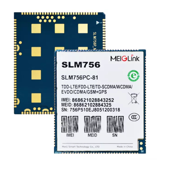
- Page 1 SLM756P User Manual Released Date:2019/3 File name: SLM756P User Manual Version Number:V1.00 Company:MeiG Smart Technology Co., Ltd MeiG Smart Technology Co., Ltd...
- Page 2 IMPORTANT NOTICE COPYRIGHT NOTICE Copyright © MeiG Smart Technology Co., Ltd. All rights reserved. All contents of this manual are exclusively owned by MeiG Smart Technology Co., Ltd(MeiG Smart for short), which is under the protection of Chineselawsandcopyrightlaws in international conventions. Anyone shall not copy, spread, distribute, modify or use in other ways with its contents without the written authorization of MeiG Smart.
- Page 3 SLM756P_Hardware Design Guide_V1.00...
- Page 4 Foreword Thank you for using the SLM756P module from Meg Smart. This product can provide data communication services. Please read the user manual carefully before use, you will appreciate its perfect function and simple operation method. The company does not assume responsibility for property damage or personal injury caused by improper operation of the user.
-
Page 5: Table Of Contents
1. Introduction ................................9 2. Module Overview ..............................9 2.1 Summary of features ............................9 2.2 Block diagram ..............................12 3. Module Encapsulation ............................. 13 3.1 Pin distribution diagram ..........................13 3.2 Pin definitions ..............................14 3.3 Mechanical Dimensions ........................... 1 4. - Page 6 6. Electrical & Reliability ............................33 6.1 Absolute Maximum ............................33 6.2 Working Temperature ............................. 33 6.3 Working Voltage............................. 34 6.4 Digital Interface Features ..........................34 6.5 SIM_VDD Characteristics ..........................34 6.6 PWRKEY Feature ............................34 6.7 VCOIN Feature .............................. 35 6.8 Current Consumption (VBAT = 3.8V) ......................
- Page 7 Version History Date Version Change description Author First edition Zheng Lei 2019-6 1.00...
-
Page 8: Introduction
2. Module Overview The SLM756P module uses the Qualcomm MSM8909 platform solution, the MSM8909 processor is manufactured in a 28nm LP CMOS process, the quad core clocked at 1.1GHz, and the memory supports 8GB+1GB (compatible with 16GB+2GB) LPDDR3. The chip can support WCDMA, FDD-LTE and other standards, and is a highly integrated product. - Page 9 A304 409.6MHz 8GB eMMC + 1GB LPDDR3/16GB eMMC + 2GB LPDDR3 System memory Android 5.1/ Android 7.1 44.0x39.0x3.0mm, 130pin Size SLM756P FDD-LTE: B2/4/5/7/12/13/17 Network (North WCDMA: B2/4/5 band America) Wi-Fi IEEE 802.11a/b/g/n 2.4G&5G Bluetooth BT4.1 Support GNSS GPS/Beidou/Glonass TDD-LTE Cat4 TDD-LTE 117/30Mbps...
- Page 10 I2C*4 For sensors/TP/others SPI*1 Master only ADC*2 Support Charging Built-in 5V/1.44A, support external charging function chip Motor Support GPIO VCOIN Real-time clock backup battery Multimode LTE main antenna Multimode LTE diversity antenna RF PIN The GPS antenna 2.4 G WiFi/BT antenna 2-way single-ended MIC (...
-
Page 11: Block Diagram
2.2 Block diagram The following figure lists the main functional parts of the module. MSM8909 Baseband PM8909 Power management Antenna interface MIPI interface Storage EMCP AUDIO interface Serial port, SD card interface, SIM card interface, I2C interface, etc. -
Page 12: Module Encapsulation
3. Module Encapsulation 3.1 Pin distribution diagram Figure 3.1:module pin diagram (top view) -
Page 13: Pin Definitions
Pin Name Pin number Description Comment The power supply The module provides four Externally, VBAT power pin pins. The SLM756P operates from a capacitor VBAT 49、50 single supply with a voltage and Zener range from 3.3V to 4.2V for diode need VBAT. - Page 14 MeiG hardware design guide MIPI_DSI0_LANE1_N MIPI_DSI0_LANE1_P MIPI_DSI0_LANE2_N MIPI_DSI0_LANE2_P MIPI_DSI0_LANE3_N MIPI_DSI0_LANE3_P LCD_RST_N LCD reset LCD_TE0 LCD frame sync signal UART UART_TX UART1 Data sent UART_RX UART1 Data reception UART_CTS UART1 Clear to send UART_RTS UART1 Request to send UART_MSM_TX UART2 Data sent debug UART_MSM_RX UART2 Data reception...
- Page 15 MeiG hardware design guide CDC_HPH_L Headphone left channel CDC_HS_DET Headphone plug detection CDC_HPH_REF Headphone reference ground CDC_EAR_P Earpiece output positive CDC_EAR_M Earpiece output negative Amplifier (0.85W) output SPKR_DRV_P Class_D positive Amplifier (0.85W) output SPKR_DRV_M Class_D negative SD Card Interface SDC2_SDCARD_DET SD card insertion detection SDC2_SDCARD_CMD SD CMD signal...
- Page 16 MeiG hardware design guide configuration GPIO8_SPI1_MOSI SPI interface GPIO9_SPI1_MISO SPI interface GPIO10_SPI1_CS SPI interface GPIO11_SPI1_CLK SPI interface Generic GPIO, without default GPIO14 configuration Generic GPIO, without default GPIO15 configuration Generic GPIO, without default GPIO16 configuration Generic GPIO, without default GPIO17 configuration Generic GPIO, without default GPIO36...
- Page 17 MeiG hardware design guide GPIO10_SPI_CS GPIO10 B-PD:nppukp Configurable I/O SPI or I2C CAM0_RST_N GPIO35* DO;B-PD:nppukp Rear camera reset; Configurable I/O CAM0_PWDN GPIO34* DO;B-PD:nppukp Rear camera pwdn;Configurable I/O CAM0_MCLK GPIO26 DO;B-PD:nppukp Rear camera clock; Configurable I/O MIPI_CSI0_LANE0_N AI, AO MIPI camera serial interface 0 lane 0 - negative MIPI camera serial interface 0 lane 0 –positive MIPI_CSI0_LANE0_P AI, AO...
- Page 18 MeiG hardware design guide VBAT PI,PO Battery VBAT PI,PO Battery VBUS USB VBUS Voltage KYPD_PWR_N Power on key RF_WIFI/BT AI,AO RF signal PM_RESIN_N PMIC reset GPIO7_I2C_SCL GPIO7 DO;B-PD:nppukp Configurable I/O I2C or GPIO GPIO6_I2C_SDA GPIO6 DO;B-PD:nppukp Configurable I/O I2C or GPIO RF_GPS RF signal-GPS ANT RF_FM...
- Page 19 MeiG hardware design guide RF_MAIN AI,AO RF signal-Main ANT UIM1_DET_N GPIO56 DI,B-PD:nppukp Configurable I/O UIM1 removal detection GPIO3 GPIO3 B-PD:nppukp Configurable I/O, MI2S_2_D1 GPIO2 GPIO2 B-PD:nppukp Configurable I/O,MI2S_2_D0 GPIO1 GPIO1 B-PD:nppukp Configurable I/O,MI2S_2_SCK GPIO0 GPIO0 B-PD:nppukp Configurable I/O,MI2S_2_WS VREG_L11_SDC PMIC output 2.95V SDC2_SDCARD_DET GPIO38* B-PD:nppukp...
- Page 20 MeiG hardware design guide MIPI display serial interface 0 lane 1 – negative MIPI_DSI0_LANE1_N AI, AO MIPI display serial interface 0 lane 1 –positive MIPI_DSI0_LANE1_P AI, AO MIPI display serial interface 0 lane 2 –negative MIPI_DSI0_LANE2_N AI, AO MIPI display serial interface 0 lane 2 –positive MIPI_DSI0_LANE2_P AI, AO GPIO36...
- Page 21 MeiG hardware design guide GPIO14 CS_N GPIO GPIO15 GPIO GPIO16 MOSI GPIO GPIO17 MISO GPIO GPIO18 CS_N GPIO GPIO19 GPIO GPIO20 MOSI GPIO GPIO21 MISO GPIO GPIO111 CS_N GPIO GPIO112 GPIO...
-
Page 22: Mechanical Dimensions
MeiG hardware design guide 3.3 Mechanical Dimensions TOP:... - Page 23 MeiG hardware design guide BOTTOM:...
- Page 24 MeiG hardware design guide Side: Figure 3.3:Recommended PCB package size (unit: mm)
-
Page 25: Interface Application
MeiG hardware design guide 4. Interface Application 4.1 Power Supply In the case of a battery device, the voltage input range of the module VBAT is 3.4V to 4.2V, and the recommended voltage is 3.8V. In the LTE band, when the module is transmitting at maximum power, the peak current can reach up to 3A, resulting in a large voltage drop on VBAT. -
Page 26: Power Pin
MeiG hardware design guide Figure 4.2:DC-DC power supply circuit Note: If the user does not use battery power, please note that a 10K resistor is connected to the 134 pin (BAT_THERM) of the module and pulled down to GND to prevent the software from judging the abnormal battery temperature after the module is turned on, resulting in shutdown. -
Page 27: Power On And Off
MeiG hardware design guide Figure 4.4:VBAT lowest voltage drop 4.2 Power on and off Do not turn on the module when the module's temperature and voltage limits are exceeded. In extreme cases, such operations can cause permanent damage to the module. 4.2.1 Module Boot The user can power up the module by pulling the PWRKEY pin (52) low. -
Page 28: Module Shutdown
15 seconds 4.2.3 Module Reset The SLM756P module supports a reset function that allows the user to quickly restart the module by pulling the module's PM_RESIN_N1 (PIN57) pin low. The RESET signal is used as the volume-key by default in Android. -
Page 29: Vcoin Power
MeiG hardware design guide Figure 4.8: Reset using the key circuit Figure 4.9:Reset Module Using External Signa When the pin is high, the voltage is typically 1.8V. Therefore, for users with a level of 3V or 3.3V, it is not possible to directly use the GPIO of the MCU to drive the pin. An isolation circuit is required. The hardware parameters of the RESET can refer to the following table: Table 4.1: RESET Hardware Parameters Description... -
Page 30: Power Output
This VCOIN power supply is typically 3.0V and consumes approximately 8uA when VBAT is disconnected. 4.4 Power Output The SLM756P has multiple power outputs. For LCD, Camera, touch panel, etc. In application, it is recommended to add parallel 33PF and 10PF capacitors to each power supply to effectively remove high frequency interference. -
Page 31: Serial Port
VREG_L8_2P9 VREG_L14_UIM1 1.75~3.337 1.8/3.3 VREG_L15_UIM2 1.75~3.337 1.8/3.3 4.5 Serial Port The SLM756P provides two serial ports for communication. UART1 with hardware flow control, UART2 default for debugging. Table 4.3: UART Pin Description Name Direction Function UART_TX UART1 Data Transmission UART_RX... - Page 32 MeiG hardware design guide Figure 4.14: TX Connection Diagram Figure 4.15: RX Connection Diagram Note: When using Levels 14 and 15 for level isolation, you need to pay attention to the output timing of VREG_L6_1P8. Only after VREG_L6_1P8 is output normally, the serial port can communicate normally.
-
Page 33: Mipi Interface
(Refer to the MIPI Alliance Specfication for D-PHY 7.6.5). 4.6.1 LCD Interface The SLM756P module supports the LCD display of the MIPI interface with an identification signal for the compatible screen. The resolution of the screen can be up to 1280*720. The signal interface is shown in the following table. -
Page 34: Power Supply
MeiG hardware design guide MIPI_DSI0_LANE2_P MIPI_DSI0_LANE3_N MIPI_DSI0_LANE3_P PM8909_MPP2 Backlight PWM ontrol signal LCD_TE Frame synchronization signal LDO6_1P8 1.8V power supply LDO17_2P85 2.85V power supply The LCD_ID of the module can use GPIO (only recognize high and low level) or ADC (PM8909_MPP4). - Page 35 4.6.2 MIFI camera Interface The SLM756P module supports the MIPI interface Camera and provides a dedicated camera power supply. The main camera is a CSI0 interface that supports two sets of data lines and can support 8M pixels. The front camera is a CSI1 interface that supports a set of data lines and can support 5M pixels.
- Page 36 MeiG hardware design guide CAM_I2C_SDA I2Csignal,CAMdedicated CAM_I2C_SCL I2Csignal,CAMdedicated VREG_L6_1P8 1.8V IOVDD VREG_L17_2P85 2.8V AVDD ) powering the focus motor VREG_L8_2P9 2.9V AFVDD( VREG_L2_1P2 1.2V DVDD If the user designs to use the CAMERA module with autofocus function, please note that the I2C of the module cannot be directly connected to the AF device.
- Page 37 MeiG hardware design guide Figure 4.19: MIPI Camera Reference Circuit When designing the camera function, you need to pay attention to the position of the connector. There will be a small person in the specification of the camera to indicate the imaging direction. You need to ensure that the villain stands on the long side of the LCD.
- Page 38 MeiG hardware design guide Figure 4.20: Camera imaging diagram 4.7 Resistive Touch Interface The module does not provide a resistive touch screen interface. If the user needs to use a resistive touch, an external dedicated chip is required. The module can provide an I2C interface.The reference circuit is as follows: Figure 4.21: RTP Reference Circuit 4.8 CapacitiveTouch Interface...
- Page 39 MeiG hardware design guide The capacitive touch I2C interface GPIO10_TP_I2C3_SDA needs to be pulled up GPIO11_TP_I2C3_SCL toVREG_L5_1P8 GPIO65_TP_INT_N Interrupt GPIO64_TP_RST_N Reset VREG_L17_2P85 2.8V Power Note: The interface definition of the capacitive touch can be adjusted by software, and the user can change the GPIO and I2C according to the design needs.
- Page 40 MeiG hardware design guide 4.9.1 Receiver Interface Circuit Figure 4.21: Receiver Interface Circuit 4.9.1 Microphone receiving Circuit Below is the MEMS microphone interface circuit, which has more BIAS power supply than the electret MIC. Figure 4.22: Microphone Differential Interface Circuit 4.9.2 Headphone Interface Circuit The module integrates a stereo headphone jack.
- Page 41 MeiG hardware design guide Figure 4.23: Headphone Interface Circuit note: 1. The earphone holder in Figure 4.23 is normally closed. If the user is using the normally open mode earphone holder, please modify the detection circuit according to the actual pin and modify the software accordingly. 2.
- Page 42 GPIO0 4.10 USB Interface The SLM756P supports a USB 2.0 High speed interface. It must control the 90 ohm differential impedance during Layout and control the external trace length according to the internal trace length of the module.The module supports OTG function at the same time (requires external circuit to provide external 5V power supply).The voltage input range during charging is as follows:...
- Page 43 Figure 4.26: USB Connection Diagram 4.10.1 USB OTG The SLM756P module provides USB OTG functionality and requires an external charging chip or power chip to output 5V power to external devices. The work The pins that can be used are as follows: Table 4.10: USB OTG Pin Description...
- Page 44 Figure 4.28: Battery connection diagram 4.11.2 Charge Control The SLM756P module can charge the over-discharged battery. The charging process includes trickle charge, constant current, and constant voltage charging. Trickle charge: it is divided into 2 parts, trickle charge-A: charge current 90mA when the battery voltage is lower than 2.8V;...
- Page 45 MeiG hardware design guide 4.12 UIM Card Interface The SLM756P can support two SIM cards at the same time to achieve dual card dual standby. Support SIM card hot swap, can automatically recognize 1.8V and 3.0V cards. The figure below shows the recommended interface circuit for the SIM card.
- Page 46 4.15 Analog to Digital Converter (ADC) The SLM756P module provides two MPP function signals from the power management chip. MPP4 is the ADC input signal and MPP2 is the PWM signal. The ADC signal is 16-bit resolution, and its performance parameters are as follows: Table 4.12: ADC Performance Parameters...
- Page 47 MeiG hardware design guide 4.17 Motor The SLM756P supports motor functions that can be implemented by the user with GPIO control power. The reference schematic is as follows: Figure 4.32: Motor interface circuit 4.18 Antenna Interface The module provides four antenna interfaces: MAIN antenna, DRX antenna, GPS antenna and WiFi/BT antenna.
- Page 48 MeiG hardware design guide In the figure, R101, C101, and C102 are antenna matching devices, and the specific component values can be determined after the antenna factory debugs the antenna. Among them, R101 defaults to 0R, C101 and C102 do not paste by default. If there are fewer components between the antenna and the module output, or if the RF test head is not needed in the design, the antenna matching circuit can be simplified as shown below: Figure 4.34: MAIN Antenna Interface Simplified Connection Circuit...
- Page 49 MeiG hardware design guide If there are fewer components between the antenna and the module output, or if the RF test head is not needed in the design, the antenna matching circuit can be simplified as shown below: Figure 4.36: DRX Antenna Interface Simplified Connection Circuit In the above figure, R102 defaults to 0R, C103 and C104 are not attached by default.
- Page 50 MeiG hardware design guide Figure 4.38: Connecting Active Antennas 4.18.4 WiFi/BT antenna The module provides the WiFi/BT antenna pin RF_WIFI/BT. The antenna on the user's motherboard should be connected to the antenna pin of the module using a 50 ohm microstrip line or strip line. In order to facilitate antenna debugging and certification testing, an RF connector and antenna matching network should be added.
- Page 51 SLM756P module is much higher than the previous 2G module, please read this chapter carefully, reduce the subsequent hardware debugging cycle. When using the SLM756P module, the user is required to use at least 4 layers of via design for the impedance control and signal line shielding.
- Page 52 MeiG hardware design guide 5.2.1. Antenna Antenna part design, SLM756P module has a total of 5 antenna interfaces, they are: RF_MAIN, RF_DRX, RF_GPS, RF_WIFI, RF_FM. Pay attention to component placement and RF routing: The RF test head is used to test the conducted RF performance and should be placed as close as possible to the antenna pins of the module;...
- Page 53 MeiG hardware design guide 5.2.4. MIPI MIPI is a high-speed signal line. Users must pay attention to protection during the layout phase, so that they are away from the signal lines that are easily interfered. The GND processing must be performed on the upper and lower sides, and the traces are differential pairs.
- Page 54 MeiG hardware design guide The LTE antenna is the main source of coupling interference for FDD, so users should pay attention to keeping the audio trace away from the LTE antenna and VBAT during PCB layout and routing. The filter capacitor of the audio is preferably placed close to the module end and placed next to the interface end.
- Page 55 MeiG hardware design guide Storage ℃ temper ature 6.3 Working Voltage Table 6.3: Module Operating Voltage Parameter Minimum Typical Maximum Unit VBAT VBUS Hardware shutdown voltage 6.4 Digital Interface Features Table 6.4: Digital Interface Features (1.8V) Parameter Description Minimum Typical Maximum Unit Input high level...
- Page 56 MeiG hardware design guide low level Effective time 2000 6.7 VCOIN Feature Table 6.6: VCOIN Characteristics Paramet Description Minimum Typical Maximum Unit VCOIN VCOIN input voltage 3.25 VCOINCurrent RTC-IN consumption VCOIN VCOIN Output voltage VCOIN Output current RTC-OUT 6.8 Current Consumption (VBAT = 3.8V) Table 6.8: Current consumption Param Descrip...
- Page 57 MeiG hardware design guide 6.9 Electrostatic Protection The module is not specifically protected against electrostatic discharge. Therefore, users must pay attention to electrostatic protection when producing, assembling, and operating modules. 6.10 Module Operating Frequency Band The table below lists the operating frequency bands of the module and complies with the 3GPP TS 05.05 technical specification.
- Page 58 MeiG hardware design guide 6.11 RF Characteristics The following table lists the conducted RF output power of the module, in accordance with 3GPP TS 05.05 technical specification, 3GPP TS 134121-1 standard. Table 6.10: Conducted Output Power 6.12 Module Conduction Receiving Sensitivity The table below lists the conducted receive sensitivity of the module and is tested under static conditions.
- Page 59 MeiG hardware design guide Table 6.11: Conducted Receive Sensitivity Receive sensitivity Frequency band Receive sensitivity (maximum) (typical) 3GPP Claim WCDMAB5 <-109 dBm 3GPP Claim TDSCDMA1.9G <-110 dBm 3GPP Claim TDSCDMA2G <-110 dBm See table 6.12 3GPP Claim LTEFDD/TDD Table 6.12: LTE Reference Sensitivity 3GPP Dual Antenna Requirements (QPSK) E-UTRA Frequency band 1.4 MHz...
- Page 60 MeiG hardware design guide -103.2 -100.2 -100.2 -98.5 -95.5 -93.7 -99.0 -95.7 -93.5 -100 -95.2 -100 -95.2 -106.2 -102.2 -100 -95.2 -106.2 -102.2 -100 -95.2 -100 -95.2 -100 -95.2 -100 -95.2 -100 -95.2 -93.2 6.13 WIFI Main RF Performance The table below lists the main RF performance under WIFI conduction. Table 6.13: Main RF performance parameters under WIFI conduction Transmission performance 802.11B...
- Page 61 MeiG hardware design guide Receiving performance Receiving sensitivity 802.11B 802.11N Minimum rate Maximum rate 6.14 BT Main RF Prformance The table below lists the main RF performance under BT conduction. Table 6.14: Main RF performance parameters under BT conduction Transmission performance 2DH5 3DH5 Target power...
- Page 62 Figure 49: Module recommended soldering furnace temperature curve 7.3. Humidity Sensitivity (MSL) The SLM756P module meets moisture sensitivity level 3. The dry package is subjected to the J-STD- 020C specification in accordance with the IPC/JEDEC standard under ambient conditions of <30...
- Page 63 96 hours at temperatures above 90 ° C and as high as 125 ° C. 7.4. Baking Requirements The MEIG Smart Module has a moisture rating of three. The SLM756P should be fully baked before reflow soldering, otherwise the module may cause permanent damage during reflow. The SLM756P can use the following three baking conditions.
- Page 64 MeiG hardware design guide ILI9881C HOLITECH ILI9881C Table 8.2: List of supported camera models Vendor Drive IC GXKJ SP5506 GXKJ SP2509 Table 8.3: List of supported touch screen models Vendor Drive IC GT5688 HOLITECH GT5688 DIXIAN GT970 Table8.4:List of supported G sensor models Vendor Model Specification...
- Page 65 MeiG hardware design guide Identification CHINA-VISION Sweeping the pier Zeba 9. Appendix 9.1. Related Documents Table 9.1: Related documents Serial File name Comment number Digital cellular telecommunications (Phase 2+); AT command set for GSM Mobile 07.07: Equipment (ME) Support GSM 07.10 multiplexing protocol 07.10:...
- Page 66 MeiG hardware design guide Circuit Switched Data Clear to Send Data Terminal Equipment (typically computer, terminal, printer) Data Terminal Ready Discontinuous Transmission Enhanced Full Rate Electrostatic Discharge European Telecommunication Standard Full Rate Half Rate IMEI International Mobile Equipment Identity Li-ion Lithium-Ion Mobile Originated Mobile Station (GSM engine), also referred to as TE...
- Page 67 MeiG hardware design guide Phone book Explanations abbreviation SIM fix dialing phonebook SIM last dialing phonebook (list of numbers most recently dialed) Mobile Equipment list of unanswered MT calls (missed calls) SIM (or ME) own numbers (MSISDNs) list Mobile Equipment list of received calls SIM phonebook Not connect 9.3.
- Page 68 MeiG hardware design guide GPIO111 CS_N GPIO GPIO112 GPIO 9.4. Safety Warning Pay attention to the following safety precautions when using or repairing any terminal or mobile phone that contains modules. The user should be informed of the following safety information on the terminal device.
- Page 69 This module can be used in POS and other equipment. The input voltage to the module should be nominally 3.5~4.2 VDC ,typical value 3.8VDC and the ambient temperature of the module should not exceed 60℃. SLM756P has four External fixed rubber antenna with max antenna gain 5dBi . If the antenna needs to be changed, the certification should be re-applied.
- Page 70 If not, a second label must be placed on the outside of the final device that contains the following text: “Contains FCC ID: 2APJ4-SLM756P” “Contains IC: 23860- SLM756P“ The FCC ID/IC can be used only when all FCC ID/IC compliance requirements are met.
- Page 71 MeiG hardware design guide devices or drivers are not available. When testing for emissions from the unintentional radiator, the transmitter shall be placed in the receive mode or idle mode, if possible. If receive mode only is not possible then, the radio shall be passive (preferred) and/or active scanning.
Need help?
Do you have a question about the SLM756P and is the answer not in the manual?
Questions and answers