Table of Contents
Advertisement
Quick Links
Click
here
for production status of specific part numbers.
MAX2771
General Description
The MAX2771 is a next-generation Global Navigation
Satellite System (GNSS) receiver covering E5/L5, L2,
E6, E1/L1 bands and GPS, GLONASS, Galileo, QZSS,
IRNSS, and BeiDou navigation satellite systems on a
single chip.
Designed on Maxim's advanced, low-power SiGe BiCMOS
process technology, the MAX2771 offers the highest
performance and integration at a low cost. Incorporated
on the chip is the complete receiver chain, including
a dual-input LNA and mixer, followed by filter, PGA,
and multi-bit ADC, along with a fractional-N frequency
synthesizer, and crystal oscillator. The total cascaded
noise figure of this receiver is as low as 1.4dB.
The MAX2771 completely eliminates the need for exter-
nal IF filters by implementing on-chip monolithic filters
and requires only a few external components to form a
complete, low-cost GNSS RF receiver solution.
The MAX2771 is the most flexible receiver on the
market. The integrated delta-sigma fractional-N frequency
synthesizer allows programming of the IF frequency within
a ±30Hz (f
= 32MHz) accuracy while operating with
XTAL
any reference or crystal frequencies that are available in
the host system. The ADC outputs CMOS logic levels with
one or two quantized bits for both I and Q channels, or up
to 3 quantized bits for the I channel. The on-chip ADCs
can be bypassed and the analog I and Q signals output
for sampling with external ADCs. An analog monitoring
feature is provided that allows simultaneous output of the
on-chip ADC samples and the I analog signal.
The MAX2771 is packaged in a 5mm x 5mm, 28-pin,
TQFN package with an exposed paddle.
Applications
● Location-Enabled Mobile Handsets
● PNDs (Personal Navigation Devices)
● Telematics (Asset Tracking, Inventory Management)
● Marine/Avionics Navigation
● Software GPS
● Laptops and Netbooks
● Surveying Equipment
● Digital Still Cameras and Camcorders
● Vehicle Tracking and Fleet Management
19-100378; Rev 0; 7/18
Multiband Universal GNSS Receiver
Benefits and Features
● Multi-Constellation Support
• GPS, Galileo, GLONASS, BeiDou, IRNSS, QZSS,
SBAS
● Multiband Support
• L1, L2, L5, E1, E5, E6, B1, B2, B3
● Programmable IF Bandwidths of 2.5MHz, 4.2MHz,
8.7MHz, 16.4MHz, 23.4MHz, 36MHz
• Supports Wide-Band Carriers for Precision
Applications (e.g., GPS L5, Galileo E5)
● Operates in Low IF or Zero IF Mode
• Programmable IF Center Frequency
● Fractional-N Synthesizer with Integrated VCO
Supports Wide Range of Reference Frequencies
● On-Chip LNAs to Support Multiple Bands
● 1.4dB Cascaded Noise Figure and 110dB of
Cascaded Gain with Gain Control Range of 59dB
from PGA
● Integrated Crystal Oscillator
● Supply Voltage Range: 2.7V to 3.3V
● 28-Pin, RoHS-Compliant, Thin QFN Lead-Free
Package (5mm x 5mm)
Ordering Information
appears at end of data sheet.
EVALUATION KIT AVAILABLE
Advertisement
Table of Contents

Summary of Contents for Maxim Integrated MAX2771
-
Page 1: General Description
ADCs. An analog monitoring feature is provided that allows simultaneous output of the on-chip ADC samples and the I analog signal. The MAX2771 is packaged in a 5mm x 5mm, 28-pin, TQFN package with an exposed paddle. Applications ●... -
Page 2: Block Diagram
MAX2771 Multiband Universal GNSS Receiver Block Diagram LANIN_HI MAX2771 LANOUT_HI MIXIN_HI FILTER VCCADC CLKOUT SHDN XTAL Maxim Integrated │ 2 www.maximintegrated.com... -
Page 3: Table Of Contents
PLL Fractional Division Ratio (0x5) ............40 Maxim Integrated │ 3... - Page 4 Figure 6. Three-Wire Interface Timing Diagram ........... . . 27 Maxim Integrated │ 4...
- Page 5 Table 16. External Component List ............. . . 49 Maxim Integrated │ 5...
-
Page 6: Absolute Maximum Ratings
, IDLE bit is 1, SHDN = high μA Shutdown mode, SHDN= low Digital Input Logic-High Measure at the SHDN pin Digital Input Logic-Low Measure at SHDN pin Idle Mode is a trademark of Maxim Integrated Products, Inc. Maxim Integrated │ 6 www.maximintegrated.com... - Page 7 MAX2771 Multiband Universal GNSS Receiver Electrical Characteristics (continued) (MAX2771 EV kit, V = 2.7V to 3.3V, T = -40°C to +85°C. Registers are set to the specified default states. LNA input is driven from a 50Ω source. All RF measurements are done in the analog output mode with ADC bypassed. PGA gain is set to GAININ = 111010 through SPI interface, unless otherwise noted.
- Page 8 MAX2771 Multiband Universal GNSS Receiver Electrical Characteristics (continued) (MAX2771 EV kit, V = 2.7V to 3.3V, T = -40°C to +85°C. Registers are set to the specified default states. LNA input is driven from a 50Ω source. All RF measurements are done in the analog output mode with ADC bypassed. PGA gain is set to GAININ = 111010 through SPI interface, unless otherwise noted.
- Page 9 ADC Integral Nonlinearity AGC enabled, 3-bit output ±0.1 Note 1: MAX2771 is production tested at T = 25ºC. User must program the registers to the specified default settings upon power-up. Note 2: Default mode of the IC. PLL is an an integer-N mode with f /16 = 1.023MHz and I...
-
Page 10: Typical Operating Characteristics
MAX2771 Multiband Universal GNSS Receiver Typical Operating Characteristics (MAX2771 EV kit, V = 2.7V to 3.3V, T = -40°C to +85°C. Registers are set to the default power-up states. LNA input is driven from a 50Ω source. LNA input has specified external matching circuit. All RF measurements are done in the analog output mode with ADC bypassed. - Page 11 MAX2771 Multiband Universal GNSS Receiver Typical Operating Characteristics (continued) (MAX2771 EV kit, V = 2.7V to 3.3V, T = -40°C to +85°C. Registers are set to the default power-up states. LNA input is driven from a 50Ω source. LNA input has specified external matching circuit. All RF measurements are done in the analog output mode with ADC bypassed.
- Page 12 MAX2771 Multiband Universal GNSS Receiver Typical Operating Characteristics (continued) (MAX2771 EV kit, V = 2.7V to 3.3V, T = -40°C to +85°C. Registers are set to the default power-up states. LNA input is driven from a 50Ω source. LNA input has specified external matching circuit. All RF measurements are done in the analog output mode with ADC bypassed.
- Page 13 MAX2771 Multiband Universal GNSS Receiver Typical Operating Characteristics (continued) (MAX2771 EV kit, V = 2.7V to 3.3V, T = -40°C to +85°C. Registers are set to the default power-up states. LNA input is driven from a 50Ω source. LNA input has specified external matching circuit. All RF measurements are done in the analog output mode with ADC bypassed.
-
Page 14: Pin Configuration
SCLK Digital Input the SCLK and output on the falling-edge of SCLK. Chip-Select Input of 3-Wire Serial Interface. Set CSN low to select device. Digital Input Set CS high when the SPI transaction is completed. Maxim Integrated │ 14 www.maximintegrated.com... - Page 15 IF Section Supply Voltage. Bypass to ground with a 100nF capacitor as close as VCCIF Power possible to the pin. VCO Supply Voltage. Bypass to ground with a 100nF capacitor as close as possible VCCVCO Power to the pin. Maxim Integrated │ 15 www.maximintegrated.com...
-
Page 16: Functional Diagrams
MAX2771 Multiband Universal GNSS Receiver Functional Diagrams LANIN_HI MAX2771 LANOUT_HI MIXIN_HI FILTER CLKOUT XTAL Maxim Integrated │ 16 www.maximintegrated.com... -
Page 17: Detailed Description
Table 1. Required Register Bit Field 1227MHz. Values Mixer REGISTER BINARY The MAX2771 includes a quadrature mixer to output low- ADDRESS RANGE VALUE IF, or zero-IF, I and Q signals. There are two inputs to the mixer; one for high-band and the other for low-band. -
Page 18: Synthesizer
The LD output provides an indication of the PLL lock values for different LO frequencies, please refer to the state. Note that the lock detector requires a reference Design Resources section of the MAX2771 product page clock in order to operate. on the Maxim Integrated website. The desired integer... -
Page 19: Programmable Gain Amplifier
The PGA gain can either be controlled autono- Configuration 1 register. See Table mously by the MAX2771 using the AGC function, or The two-sided 3dB corner bandwidth can be selected be directly controlled by the host through programming of the GAININ bits in the Configuration 3 register. The to be 2.5MHz, 4.2MHz, 8.7MHz, 16.4MHz, 23.4MHz, or... -
Page 20: Adc
MAX2771 Multiband Universal GNSS Receiver Table 9. ADC Output Data Format Settings The MAX2771 features an on-chip ADC to digitize the FORMAT down-converted GNSS signal. The ADC supports the ADC OUTPUT DATA (CONFIGURATION 2 digital output in three different formats: unsigned binary,... -
Page 21: Figure 1. Adc Quantization Levels For 2 And 3-Bit Cases
MAX2771 Multiband Universal GNSS Receiver T = 1 Figure 1. ADC Quantization Levels for 2 and 3-Bit Cases Maxim Integrated │ 21 www.maximintegrated.com... -
Page 22: Adc Fractional Clock Divider
ADC clock. Alternatively, the source of the clock tional division ratio cannot exceed 0.5. This divider can may not necessarily be a MAX2771 but could be some be enabled or bypassed by using the FCLKIN bit in clock source elsewhere in the system. -
Page 23: Figure 2. Dsp Interface Top Level Connectivity And Control Signals
DATA_SYNC BIT 3 TIME_SYNC STRM_EN STRM_EN STRM_START STRM_STOP STRM_COUNT<2:0> CONTROL SIGNALS DIEID<1:0> FROM 3-WIRE INTERFACE STRM_BITS<1:0> FRM_COUNT<27:0> STAMP_EN DAT_SYNCEN TIME_SYNCEN STRM_RST CLK_ADC CLK_SER CLK_ADC CLK_SER Figure 2. DSP Interface Top Level Connectivity and Control Signals Maxim Integrated │ 23 www.maximintegrated.com... -
Page 24: Reference Clock
ADC_CLKIN pin. This tional division ratio cannot exceed 0.5. This divider can be feature allows multiple MAX2771 devices connected to a enabled or bypassed by setting the PREFRACDIV_SEL common baseband IC to have synchronized ADC outputs. -
Page 25: Serial Interface
MAX2771 tri-states SDATA, and the host subsequently 13th bit transferred from master to MAX2771 is the R/W brings CSN high completing the transaction. bit. If R/W = 1, the transaction is a read and the MAX2771 Maxim Integrated │ 25 www.maximintegrated.com... -
Page 26: Figure 4. Register Read Functional Timing
CSN high completing the transaction. register address preceded by 8 zeros and starts toggling If the host does not assert CSN, the MAX2771 will SCLK. The MAX2771 samples the bits on SDATA on the ignore any activity on SCLK or SDATA. This allows multiple rising edge of SCLK. -
Page 27: Figure 6. Three-Wire Interface Timing Diagram
SCLK falling edge to SDATA tri-stated SCLK falling edge to SDATA active Last SCLK rising edge to rising edge of CSN SCLK falling edge to data out propagation delay CSN rising edge to next SPI transaction CSN falling edge CSNOFF Maxim Integrated │ 27 www.maximintegrated.com... -
Page 28: Register Map
TIME DATA STAM Configuration 3[7:0] RESERVED[1:0] STRMBITS[1:0] MRST PLL Configuration[31:24] REFDIV[2:0] LOBAND SERVED SERVED SERVED OUTEN Configuration[23:16] RESERVED[1:0] IXTAL[1:0] RESERVED[4:2] SERVED 0x03 PLL Configuration[15:8] RESERVED[1:0] RESERVED[2:0] SERVED SERVED PLL Configuration[7:0] RESERVED[2:0] INT_PLL SERVED SERVED SERVED Maxim Integrated │ 28 www.maximintegrated.com... - Page 29 REFCLK_M_CNT[3:0] FCLKIN ADCCLK MODE [7:0] SERVED Test Mode 1[31:24] RESERVED[1:0] RESERVED[3:0] SERVED SERVED Test Mode 1[23:16] RESERVED[3:0] RESERVED[3:0] 0x08 Test Mode 1[15:8] RESERVED[3:0] RESERVED[4:2] SERVED Test Mode 1[7:0] RESERVED[1:0] SERVED SERVED SERVED SERVED SERVED SERVED Maxim Integrated │ 29 www.maximintegrated.com...
- Page 30 Test Mode 2[7:0] RESERVED[4:0] SERVED SERVED SERVED Clock Configuration 2 RESERVED[2:0] ADCCLK_L_CNT[11:8] [31:24] SERVED Clock Configuration 2 ADCCLK_L_CNT[7:0] [23:16] 0x0A Clock Configuration 2 ADCCLK_M_CNT[11:4] [15:8] CLK- Clock Configuration 2 ADCCLK_M_CNT[3:0] FRAC OUT_ RESERVED[1:0] [7:0] DIV_SEL Maxim Integrated │ 30 www.maximintegrated.com...
-
Page 31: Register Details
Mixer pole selection. Set to 1 to put the pas- 0x0: Mixer pole at 13MHz MIXPOLE sive filter pole at mixer output at 36MHz or set 0x1: Mixer pole at 36MHz to 0 to put the pole at 13MHz. Maxim Integrated │ 31 www.maximintegrated.com... - Page 32 0x0: 5th order filter F3OR5 Filter order selection 0x1: 3rd order filter 0x0: Lowpass filter FCENX Polyphase filter selection 0x1: Complex bandpass filter 0x0: Filter gain reduced 6dB FGAIN IF filter gain setting 0x1: Normal filter gain Maxim Integrated │ 32 www.maximintegrated.com...
-
Page 33: Configuration 2 (0X1)
AGC gain reference value expressed by the GAINREF 26:15 number of MSB counts (magnitude bit density) 0x0: Nothing applied SPI_SDIO_ 0x1: Pull-down resistor applied 14:13 SPI SDIO pin configuration when tri-stated CONFIG 0x2: Pull-up resistor applied 0x3: Bus-hold applied Maxim Integrated │ 33 www.maximintegrated.com... - Page 34 DRVCFG output driver configuration 0x2: Analog outputs (ADC bypass mode) 0x3: Analog outputs (ADC bypass mode) RESERVED Reserved: DO NOT CHANGE VALUE RESERVED RESERVED Reserved: DO NOT CHANGE VALUE RESERVED DIEID Identifies version of IC Maxim Integrated │ 34 www.maximintegrated.com...
-
Page 35: Configuration 3 (0X2)
Reserved: DO NOT CHANGE VALUE RESERVED RESERVED Reserved: DO NOT CHANGE VALUE RESERVED Enable of highpass coupling between filter 0x0: Disable coupling FHIPEN and PGA. 0x1: Enable coupling RESERVED Reserved: DO NOT CHANGE VALUE RESERVED Maxim Integrated │ 35 www.maximintegrated.com... - Page 36 Each pulse is coincident with the SYNCEN beginning of the 16-bit data word that cor- responds to a given output bit. This command resets all the counters irre- STRMRST spective of the timing within the stream cycle. Maxim Integrated │ 36 www.maximintegrated.com...
-
Page 37: Pll Configuration (0X3)
0x1: L2/L5 band RESERVED Reserved: DO NOT CHANGE VALUE RESERVED RESERVED Reserved: DO NOT CHANGE VALUE RESERVED RESERVED Reserved: DO NOT CHANGE VALUE RESERVED 0x0: Disable clock buffer REFOUTEN Output clock buffer enable 0x1: Enable clock buffer Maxim Integrated │ 37 www.maximintegrated.com... - Page 38 PLL mode. 0x1: Integer-N PLL 0x0: Disable PLL power-save mode PWRSAV Enable PLL power-save mode 0x1: Enable PLL power-save mode RESERVED Reserved: DO NOT CHANGE VALUE RESERVED RESERVED Reserved: DO NOT CHANGE VALUE RESERVED Maxim Integrated │ 38 www.maximintegrated.com...
-
Page 39: Pll Integer Division Ratio (0X4)
Write, Read Write, Read BITFIELD BITS DESCRIPTION DECODE RESERVED 31:28 Reserved: DO NOT CHANGE VALUE RESERVED NDIV 27:13 PLL integer division ratio RDIV 12:3 PLL reference division ratio RESERVED Reserved: DO NOT CHANGE VALUE RESERVED Maxim Integrated │ 39 www.maximintegrated.com... -
Page 40: Pll Fractional Division Ratio (0X5)
RESERVED Reserved: DO NOT CHANGE VALUE RESERVED RESERVED Reserved: DO NOT CHANGE VALUE RESERVED RESERVED Reserved: DO NOT CHANGE VALUE RESERVED RESERVED Reserved: DO NOT CHANGE VALUE RESERVED RESERVED Reserved: DO NOT CHANGE VALUE RESERVED Maxim Integrated │ 40 www.maximintegrated.com... -
Page 41: Reserved (0X6)
RESERVED[15:8] Reset 0x8000000 Access Type Write, Read Field RESERVED[7:0] Reset 0x8000000 Access Type Write, Read BITFIELD BITS DESCRIPTION DECODE RESERVED 31:28 Reserved: DO NOT CHANGE VALUE RESERVED RESERVED 27:0 Reserved: DO NOT CHANGE VALUE RESERVED Maxim Integrated │ 41 www.maximintegrated.com... -
Page 42: Clock Configuration 1 (0X7)
0x1: Take ADC clock from fractional divider 0x0: Use output of reference clock divider/multiplier ADCCLK ADC clock selection 0x1: Bypass reference clock divider/multiplier RESERVED Reserved: DO NOT CHANGE VALUE RESERVED MODE DSP interface mode selection Maxim Integrated │ 42 www.maximintegrated.com... -
Page 43: Test Mode 1 (0X8)
RESERVED Reserved: DO NOT CHANGE VALUE RESERVED RESERVED Reserved: DO NOT CHANGE VALUE RESERVED RESERVED Reserved: DO NOT CHANGE VALUE RESERVED RESERVED Reserved: DO NOT CHANGE VALUE RESERVED RESERVED Reserved: DO NOT CHANGE VALUE RESERVED Maxim Integrated │ 43 www.maximintegrated.com... -
Page 44: Test Mode 2 (0X9)
12:8 Reserved: DO NOT CHANGE VALUE RESERVED RESERVED Reserved: DO NOT CHANGE VALUE RESERVED RESERVED Reserved: DO NOT CHANGE VALUE RESERVED RESERVED Reserved: DO NOT CHANGE VALUE RESERVED RESERVED Reserved: DO NOT CHANGE VALUE RESERVED Maxim Integrated │ 44 www.maximintegrated.com... -
Page 45: Clock Configuration 2 (0Xa)
Sets the value for the M counter M_CNT 0x0: Bypass fractional clock divider FRACDIV_ Fractional clock divider selection 0x1: Enable fractional divider CLKOUT_ 0x0: Integer divider/multiplier output CLKOUT selection 0x1: ADC clock RESERVED Reserved: DO NOT CHANGE VALUE RESERVED Maxim Integrated │ 45 www.maximintegrated.com... -
Page 46: Applications Information
TXCO clock by 2 giving an ADC clock DC. For the case of the GPS L1 P(Y) signal, the required frequency of 32.7MHz. LO frequency is 1575.42MHz. As an example, assume the TXCO frequency is 16.368 MHz. Assume the PLL Maxim Integrated │ 46 www.maximintegrated.com... -
Page 47: Determining Agc Gain Setpoint
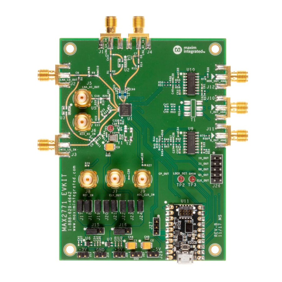
PCB Layout Considerations application note General Layout Guidelines for RF and Mixed-Signal PCBs, available on the MAX2771 product The MAX2771 EV kit can be used as a starting point for page for more information. layout. For best performance, take into consideration grounding and routing of RF, baseband, and power Maxim Integrated │... -
Page 48: Typical Application Circuit
MAX2771 Multiband Universal GNSS Receiver Typical Application Circuit Circuit 1 LANIN_HI MAX2771 LANOUT_HI MIXIN_HI FILTER VCCADC CLKOUT SHDN REFERENCE CLOCK OUTPUT XTAL REFERENCE CLOCK INPUT Maxim Integrated │ 48 www.maximintegrated.com... -
Page 49: External Component List
1.7 pF RF matching capacitor for high-band LNA input 1.1 pF RF matching capacitor for low-band LNA input Ordering Information PART NUMBER TEMP RANGE PIN-PACKAGE MAX2771ETI+ -40°C to +85°C 28 TQFN-EP* +Denotes a lead(Pb)-free/RoHS-compliant package. *EP = Exposed pad. Maxim Integrated │ 49 www.maximintegrated.com... -
Page 50: Revision History
Maxim Integrated cannot assume responsibility for use of any circuitry other than circuitry entirely embodied in a Maxim Integrated product. No circuit patent licenses are implied. Maxim Integrated reserves the right to change the circuitry and specifications without notice at any time. The parametric values (min and max limits) shown in the Electrical Characteristics table are guaranteed.
Need help?
Do you have a question about the MAX2771 and is the answer not in the manual?
Questions and answers
Hi everyone! i want to use differential analog output ANAINOUT ANAIPOUT in my development. Does anyone know its electrical parameters (common mode and differential voltage, permissible current, etc.)