Table of Contents
Advertisement
Quick Links
Advertisement
Table of Contents

Summary of Contents for ozQRP DDS VFO 2
- Page 1 DDS VFO 2 ONSTRUCTION ANUAL DDS VFO 2 Construction Manual – Issue 1 Page 1...
- Page 2 If these are not available then at least ensure you have discharged yourself by touching an earthed metal surface. Try not to directly touch the pins of the devices. Ensure your soldering iron has an earthed tip. DDS VFO 2 Construction Manual – Issue 1 Page 2...
-
Page 3: Table Of Contents
Voltage display calibration ........................23 10 Notes ..................................24 10.1 Overclocking ..............................24 10.2 DDS output ..............................24 10.3 Frequency range ............................24 10.4 LCD ................................... 24 10.5 Firmware upgrades ........................... 24 DDS VFO 2 Construction Manual – Issue 1 Page 3... - Page 4 Figure 3 LCD, Rotary Encoder and Power Supply ....................9 Figure 4 Component overlay ............................ 14 Figure 5 Installing in a MST ............................20 Figure 6 MST3 cable ..............................21 Figure 7 LCD operating display ..........................22 DDS VFO 2 Construction Manual – Issue 1 Page 4...
-
Page 5: Introduction
NTRODUCTION The DDS VFO 2 is designed as a companion for the MST3 transceiver board although it could be used with many other Superhet or Direct Conversion radios. It is simple to use having only one control yet offers many advanced features. A kit of parts, with the DDS chip already loaded onto PCB and blue backlit LCD, is available from www.ozQRP.com. -
Page 6: Circuit Description
The incoming power supply is regulated to 5V by a 7805 1A regulator which mounts flat on the PCB to act as a heatsink. DDS VFO 2 Construction Manual – Issue 1 Page 6... -
Page 7: Figure 1 Cpu
Figure 1 CPU DDS VFO 2 Construction Manual – Issue 1 Page 7... -
Page 8: Figure 2 Dds Generator
Figure 2 DDS generator DDS VFO 2 Construction Manual – Issue 1 Page 8... -
Page 9: Figure 3 Lcd, Rotary Encoder And Power Supply
Figure 3 LCD, Rotary Encoder and Power Supply DDS VFO 2 Construction Manual – Issue 1 Page 9... -
Page 10: Kit Supplied Parts List
2 pin plug + pins 12mm long 3mm nylon spacer 2.5mm x 20mm screws 2.5mm nuts 16 way SIL male pin header 16 way SIL female pin header 3mm x 10mm screw 3mm nut DDS VFO 2 Construction Manual – Issue 1 Page 10... -
Page 11: The Dds Vfo And The Superhet
The DDS output frequency will now become 10.0003MHz - 7.100MHz = 2.9003MHz, and the final transmitted signal will be 10.0003MHz - 2.9003MHz = 7.100MHz. The displayed frequency now correctly matches the transmitted signal frequency. DDS VFO 2 Construction Manual – Issue 1 Page 11... -
Page 12: Construction
Step 3: Capacitors Install the capacitors with minimal lead length. The electrolytic is the only polarized capacitor and the positive lead points towards the edge of the PCB. DDS VFO 2 Construction Manual – Issue 1 Page 12... - Page 13 The LCD can then be mounted onto the DDS VFO and mate with the 16 way male pin header. Place four 12mm long nylon spacers between the LCD and DDS VFO PCB at each corner and secure the assembly with 2.5mm screws and nuts. DDS VFO 2 Construction Manual – Issue 1 Page 13...
-
Page 14: Figure 4 Component Overlay
Figure 4 Component overlay DDS VFO 2 Construction Manual – Issue 1 Page 14... -
Page 15: First Time Power On
As the DDS VFO has not been configured the LCD will display default settings. These are frequency of 7.1MHz and a 1KHz Step. Verify with an oscilloscope or a frequency counter that the DDS is outputting a 2.9MHz sine wave signal of around 300mV pk-pk. DDS VFO 2 Construction Manual – Issue 1 Page 15... -
Page 16: Configuration
IF frequencies. Using these values the DDS VFO firmware automatically adjusts the output frequency when sidebands are changed. DDS VFO 2 Construction Manual – Issue 1 Page 16... - Page 17 When the IF Offset option is set to No the DDS VFO displayed frequency is the same as the transmit frequency. This option allows the initial frequency to be set. DDS VFO 2 Construction Manual – Issue 1 Page 17...
-
Page 18: Using The Rotary Encoder
Pressing the encoder button for less than 1 second will step the cursor onto the next digit. Once completed press the encoder button for longer than 1 second and release. DDS VFO 2 Construction Manual – Issue 1 Page 18... - Page 19 1 second will toggle the plus/minus sign. Once completed press the encoder button for longer than 1 second and release. 12. The DDS VFO will then store the values in non-volatile memory and return to normal operation. DDS VFO 2 Construction Manual – Issue 1 Page 19...
-
Page 20: Installing In Amst
The general mounting arrangement is shown in Figure 5. 10mm x 3mm tapped 12mm x 3mm tapped nylon spacer nylon spacer 3mm x 16mm C/S screw 3mm x 6mm screw Front panel Figure 5 Installing in a MST DDS VFO 2 Construction Manual – Issue 1 Page 20... -
Page 21: Wiring
USB/LSB Figure 6 MST3 cable 8.4 O UTPUT The DDS VFO output is via a 2 pin connector. The ground pin is indicated with a ‘G’ on the PCB overlay. DDS VFO 2 Construction Manual – Issue 1 Page 21... -
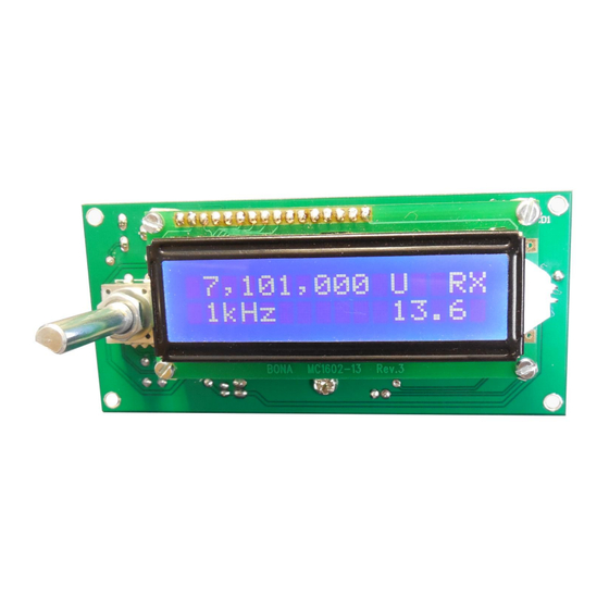
Page 22: Operation
The power supply voltage is displayed in the lower right hand side of the LCD. This is updated every 500mS. If the voltage falls below 8V a low voltage warning message is displayed to indicate the power supply is too low for proper operation. DDS VFO 2 Construction Manual – Issue 1 Page 22... -
Page 23: Frequency Calibration
4. Pressing the encoder button for less than 1 second will toggle the sign indicator. 5. Rotating the encoder will increase or decrease the difference value. 6. Once set press the encoder button for longer than 1 second. DDS VFO 2 Construction Manual – Issue 1 Page 23... -
Page 24: Notes
A non-backlit display will also not be as deep and this needs to be taken into account when mounting to the front panel. 10.5 F IRMWARE UPGRADES The PCB contains a functioning 6 pin ISP header to allow future firmware upgrades. DDS VFO 2 Construction Manual – Issue 1 Page 24...
Need help?
Do you have a question about the DDS VFO 2 and is the answer not in the manual?
Questions and answers