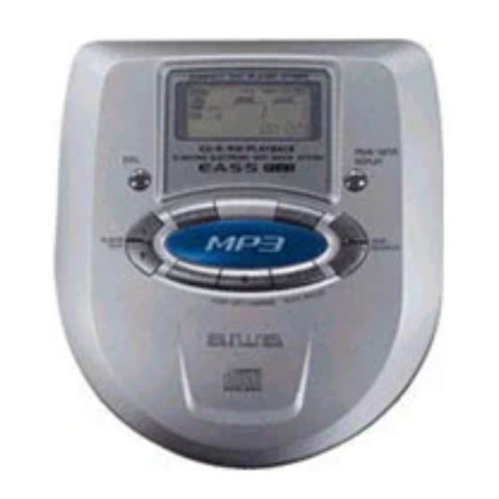
Aiwa XP-MP3 Service Manual
Hide thumbs
Also See for XP-MP3:
- Operating instructions manual (28 pages) ,
- Operating instructions manual (146 pages) ,
- Service manual (38 pages)

Related Manuals for Aiwa XP-MP3


Summary of Contents for Aiwa XP-MP3
- Page 1 XP-MP3 AU, AEZ SER VICE MANUAL COMPACT DISC PLAYER BASIC CD MECHANISM : DA23LN S/M Code No. 09-00A-350-5N2...
-
Page 2: Specification
SPECIFICATION <AU> • Design and specifications are subject to change without notice. SPECIFICATION <AEZ> Tracking system 3-beam laser «AC Adaptor AC-A56E» Laser pickup Semiconductor laser Rated input AC 230 V, 50 Hz D/A conversion Multi-bit DAC Supplied headphones HP-M043 Frequency response Type: In-ear type 20 –20,000 Hz (47 k ohms) Impedance: 16 ohms... -
Page 3: Protection Of Eyes From Laser Beam During Servicing
PROTECTION OF EYES FROM LASER BEAM DURING SERVICING This set employs laser. Therefore, be sure to follow carefully the CAUTION instructions below when servicing. Use of controls or adjustments or performance of procedures other than those specified herein may result in hazardous WARNING! radiation exposure. -
Page 4: Accessories List
ACCESSORIES LIST REF. NO PART NO. KANRI DESCRIPTION 1 8A-HP1-905-010 IB,EZ(6L)S<AEZ> 1 8A-HP1-901-010 IB,U(3L)S<AU> 2 87-B30-124-110 HEADPHONE,HP-M028<AU> 2 87-B30-265-010 HEADPHONE,HP-M043<AEZ> ! ! ! ! ! 3 87-042-207-010 AC ADAPTOR,AC-A56 U<AU> ! ! ! ! ! 3 87-042-210-210 AC ADAPTOR,AC-A56E<AEZ> 4 86-YK1-001-310 ADAPTOR,CAP-6<AU>... -
Page 5: Electrical Main Parts List
ELECTRICAL MAIN PARTS LIST - 1/3 REF. NO PART NO. KANRI DESCRIPTION REF. NO PART NO. KANRI DESCRIPTION C0208 87-A10-504-080 C-CAP,U 0.047-16 K B C0209 87-012-199-080 C-CAP,U 220P-50 J CH 8A-HP1-607-010 C-IC,UPD784216AYGC-105-8EU C0210 87-A10-827-080 C-CAP,U 0.47-6.3 K B 87-A21-941-030 C-IC,UT62L1024LC-70LL C0211 87-010-831-080 C-CAP,U 0.1-16 Z F... - Page 6 ELECTRICAL MAIN PARTS LIST - 2/3 REF. NO PART NO. KANRI DESCRIPTION REF. NO PART NO. KANRI DESCRIPTION C0539 87-010-831-080 C-CAP,U 0.1-16 Z F J0501 87-A61-447-010 JACK,DC DJ26B BLK 6 C0540 87-010-831-080 C-CAP,U 0.1-16 Z F J0801 87-A61-446-010 JACK,3.5 GRN ST W/REM C0541 87-012-274-080 C-CAP,U 1000P-50 K B...
- Page 7 ELECTRICAL MAIN PARTS LIST - 3/3 • Regarding connectors, they are not stocked as they are not the initial order items. The connectors are available after they are supplied from connector manufacturers upon the order is received. CHIP RESISTOR PART CODE Chip Resistor Part Coding Figure Resistor Code...
-
Page 8: Transistor Illustration
TRANSISTOR ILLUSTRATION 2SA1162 2SB1412 UMH4N 2SA1586 2SC4116 CPH3106 CPH3206 RN1302 RN1308 RN1311 RN2311... - Page 9 SCHEMATIC DIAGRAM - 1 (MAIN-1/2 SECTION) VC1.5V 3.1V VC1.5V (SLCON) 3.1V 3.1V Q505 DC/DC CONVERTER(SW) 3.1V DC/DC CONVERTER 3.4V MP3 POWER SW 3.0V 3.1V DC/DC CONVERTER 3V REGULATOR LR6(AA)
- Page 10 SCHEMATIC DIAGRAM - 2 (MAIN-2/2 SECTION) 3.4V 3.4V PR SIG MAKE CIRCUIT 3.1V 3.1V 105-8EU START MODE OP/CL <AU>: 3.3 <AEZ>: 12 3.0V <AU>: 3.3 <AEZ>: 12 1.25V 3.4V 3.4V 3.0V 3.1V 3.1V 3.0V TO LCD C.B CN901 VIA FFC1 -10-...
- Page 11 WIRING - 1 (MAIN C.B 1/2) This wiring diagram show a 4-layer boards. a ~ g marks show the connections between the usual double-face patterns and the patterns on the internal layers that cannot be seen. The patterns with marks are connected to +B patterns. The patterns with marks are connected to GND patterns.
- Page 12 WIRING - 1 (MAIN C.B 2/2) This wiring diagram show a 4-layer boards. a ~ g marks show the connections between the usual double-face patterns and the patterns on the internal layers that cannot be seen. The patterns with marks are connected to +B patterns. The patterns with marks are connected to GND patterns.
- Page 13 SCHEMATIC DIAGRAM - 3 (LID SECTION) -13-...
- Page 14 WIRING - 2 (LID C.B) -14-...
- Page 15 WAVEFORMS - 1/2 IC201 Pin 67 (BCK) IC251 Pin 17 (RF O) 1V/200ns DIV 500mV/200ns DIV IC251 Pin 14 (TA O) IC201 Pin 66 (PCMD) 50mV/1ms DIV 1V/1µs DIV IC251 Pin 16 (FE O) IC201 Pin 65 (LRCK) 50mV/1ms DIV 1V/10µs DIV IC201 Pin 71 (XTAI) IC201 Pin 25 (MDP)
- Page 16 WAVEFORMS - 2/2 IC651 Pin 27 (SDATA) IC601 Pin 26 (SOC) 1V/200ms DIV 1V/200ns DIV IC701 Pin 14 (CLKO) (14.725MHz) IC601 Pin 14 (PR) 1V/50ns DIV 1V/:50µs DIV IC601 Pin 24 (SOD) 1V/:5µs DIV IC601 Pin 25 (SOI) 1V/20µs DIV -16-...
-
Page 17: Test Mode
TEST MODE - 1/2 The servo circuit in this model does not need adjustment: It is entirely controlled inside an IC. Therefore, each time TOC is read, adjustment and disc detection will automatically be performed. Do not use MP3 recorded discs in the test mode. 1. - Page 18 TEST MODE - 2/2 (2) Tracking balance/gain check Press the PRGM button during playback of disc: The display in the LCD will switch from F-BIAS to T-BAL, T-GAIN, and to playback time. Playback time display Tracking gain Focus bias Tracking bias (adjustment value is not displayed) * Caution: Since the adjustment values are determined inside the IC, they will vary depending on the disc: Only the displayed values will be checked for adjustment.
-
Page 19: Ic Block Diagram
IC BLOCK DIAGRAM - 1/3 IC, SN74LV244APW IC, S-80825ANNP-EDN Vref 3 NC INPUTS OUTPUT H : Hight Level L : Low Level X : Unless specified Z : Hight Impedance IC, CXA1791N LDON FE BIAS 1.25V -19-... - Page 20 IC BLOCK DIAGRAM - 2/3 IC, BH6508FS IN-SP CN-SP O-SPF O-SPR O-SLR O-SLF CN-SL IN-SL 3.75k Thermal shut down H BRIDGE4 H BRIDGE3 LOGIC4 LOGIC4 DRIVER4 DRIVER3 LOGIC1 LOGIC2 DRIVER1 DRIVER2 H BRIDGE1 H BRIDGE2 VREF IN-FO CN-FO O-FOF O-FOR O-TOR O-TOF CN-TO IN-TO VREF...
- Page 21 IC BLOCK DIAGRAM - 3/3 IC, S8324A33MC-EON-T2 VOUT VREF CONTROL SOFT START (ON/OFF) IC, AK4352VT DIF0 DIF1 EMPH LRCK Serial Input De-emphasis VCML Interface DATA Control ∑ OUTL Interpolator Modulator ∑ OUTR Interpolator Modulator Clock Divider VCMR VREF IC, TA2120FN BIAS BEEP BIAS...
- Page 22 IC DESCRIPTION - 1/6 (µPD784216AYGC-105-8EU) - 1/3 Pin No. Pin Name Description CHARGE Goes "H" to start charging. P-OFF Outputs one-shot "L" (approx. 50 ms) to turn off the CD system power. WAKE UP Outputs one-shot "H" (approx. 50 ms) to turn on the CD system power. LCD RST Reset output to LCD driver ECLK...
- Page 23 IC DESCRIPTION - 1/6 (µPD784216AYGC-105-8EU) - 2/3 Pin No. Pin Name Description DECRST RESET output to ROM decoder AVREF1 ─ Connected to VDD since D/A converter is not used. DEBUG1 DEBUG2 For debugging ("L" when hyper terminal is not used) DEBUG3 ̲̲̲̲̲̲̲̲̲̲̲̲̲ MP3ON Data switching output. "H": CD-DA; "L": MP3 ─ Not used ̲̲̲̲̲̲̲ STNBY Standby output to H.PAMP. "H": ON; "L": STANDBY ̲ DSL1/2 DSL1/2 switching output. "H": DSL1; "L": DSL2 BEEP BEEP output to H.PAMP C DATA A-MUTE MUTE output to H.PAMP. "H": MUTE C CLOCK 48 〜 55 A0 〜...
- Page 24 IC DESCRIPTION - 1/6 (µPD784216AYGC-105-8EU) - 3/3 Pin No. Pin Name Description EMPH EMPHASIS ON/OFF output to DAC. "H": ON; "L": OFF PICKUP-SEL Pickup select pin. "H": DA-23L; "L": DA-23LN SW-EASS MODE SW detection. "H": NORMAL; "L": QUICK. ACIN AC adapter input detection. "H": With input; "L": Without input. IC, µPD784216AYGC-105-8EU A/D input set values: Reference voltages in ( ) with VDD 3.1 V K-FUNC1 K-FUNC2...
- Page 25 IC DESCRIPTION - 2/6 (SM5904BF) - 1/1 Pin No. Pin Name Description VDD2 – input; "L": Without input ________ Power supply EASSON RF peaking SW switching output. "L": EASS ON CDRW _____ LDON CDRW SW switching output. "H": CD-RW mode VGMUTE Pickup laser ON/OFF switching output. "L": Laser ON Driver VG voltage ON/OFF switching output. "H": VG power ON – – Connect to ground _____ TEST – Not used MCLK – 16.9344MHz clock input DATAI Connect to ground Audio serial data input LRCKI Audio serial input (LR clock data) BCKI...
- Page 26 IC DESCRIPTION - 3/6 (MAS3507D-G10) - 1/2 Pin No. Pin Name Description Test enable _______ Reset, active “L” 12CC C clock low 12CD C data line – Positive supply for digital parts – Ground supply for digital parts DCEN Enable DC/DCconverter _______ PIO end of DMA, active “L”...
- Page 27 IC DESCRIPTION - 3/6 (MAS3507D-G10) - 2/2 Pin No. Pin Name Description Start-up 1): Enable layer 3/Disable layer 3 decoding, Operation 2): MPEG header bit 20 (Sampling frequency) Start-up 1): Enable layer 2/Disable layer 2 decoding, PI12 Operation 2): MPEG header bit 21 (Sampling frequency) Start-up 1): SDO: select 32-bit mode/16-bit I S mode PI11...
- Page 28 IC DESCRIPTION - 4/6 (LC89513K) - 1/1 Pin No. Pin Name Description – Ground 2 ~ 8 RA0 ~ RA6 Address signal outputs to data buffer RAM – Ground 10 ~ 16 RA7 ~ RA13 Address signal outputs to data buffer RAM –...
- Page 29 IC DESCRIPTION - 5/6 (CXD2585Q) - 1/2 Pin No. Pin Name Description – Digital power supply XRST System reset. Rest at “L”. MUTE Muting input. Mute at “H”. DATA Serial data input from CPU XLAT Latch input from CPU. Latched at falling edge. CLOK Serial data transfer clock input from CPU SENS...
- Page 30 IC DESCRIPTION - 5/6 (CXD2585Q) - 2/2 Pin No. Pin Name Description Tracking error signal input Middle point servo analog input RFDC RF signal input ADIO Testing pin (Not used) AGND – Analog GND IGEN Constant current input for OP amplifier AVDD – Analog power supply ASYO EFM full swing output “L”...
- Page 31 IC DESCRIPTION - 6/6 (DAC3550A-C2) - 1/2 Pin No. Pin Name Description AGNDC Analog reference voltage AVSS1 VSS 1 for audio back-end. AVSS0 VSS 0 for audio output amplifiers. – Not used OUTL Audio output: Headphone left or speaker + –...
- Page 32 IC DESCRIPTION - 6/6 (DAC3550A-C2) - 2/2 Pin No. Pin Name Description FOPR Right filter op amp inverting input FINR Input for FOUTR or filter op amp output (line out) VREF Analog reference ground -32-...
-
Page 33: Mechanical Exploded View
MECHANICAL EXPLODED VIEW 1/1 DAN23LN -33-... - Page 34 MECHANICAL MAIN PARTS LIST 1/1 REF. NO PART NO. KANRI DESCRIPTION 1 8A-HP1-009-010 PANEL,LID CD 2 8A-HP1-007-010 WINDOW,DISPLAY<AEZ> 2 8A-HP1-018-010 WINDOW,DISPLAY MP3C<AU> 3 8A-HP1-001-010 LID,CD 4 8A-HP1-609-010 LCD,AHP-1 5 8A-HP1-202-010 GUIDE,LCD 6 8A-HP1-008-010 HLDR,PWB LID 7 8A-HP1-005-010 KEY,PLAY 8 8A-HP1-006-010 KEY,MODE 9 8A-HP1-205-010 SPR-T,LID(L)
-
Page 35: Color Name Table
COLOR NAME TABLE COLOR NAME TABLE Basic color symbol Color Basic color symbol Color Basic color symbol Color Black Cream Orange Green Gray Blue Transparent Blue Gold Pink Silver Titan Silver Brown Violet White Transparent White Yellow Transparent Yellow Metallic Blue Light Blue Transparent Green Dark Blue... -
Page 36: Mechanism Exploded View
MECHANISM EXPLODED VIEW 1/1 <DA23LN> -36-... - Page 37 MECHANISM MAIN PARTS LIST 1/1 <DA23LN> REF. NO PART NO. KANRI DESCRIPTION 1 S0-A41-A20-604 PICKUP ASSY LASER P200L 2 S0-M10-A10-800 MOTOR SPINDLE ASSY 3 S0-M10-A10-900 MOTOR SLED ASSY 4 S2-311-A12-200 CHASSIS 5 S2-511-A23-200 GEAR MIDDLE 6 S2-511-A23-100 GEAR,SCREW 7 S2-511-A23-400 GEAR,RACK 8 S2-511-A07-901 SPINDLE SCREW...
- Page 38 2–11, IKENOHATA 1–CHOME, TAITO-KU, TOKYO 110-8710, JAPAN TEL:03 (3827) 3111 920074 Printed in Singapore...
Need help?
Do you have a question about the XP-MP3 and is the answer not in the manual?
Questions and answers