Table of Contents
Advertisement
Advertisement
Table of Contents

Related Manuals for Inventec B800

Summary of Contents for Inventec B800
- Page 1 About This Manual Board B800 May, 2012 (Revision A,1)
-
Page 2: Copyright Notice
No one may, transmit, adapt, assign, compile, rent, sale, change, copy, reproduce, distribute, publish, display, broadcast, or use in any way the content of this manual, in whole or in part, for any other purpose whatsoever without the prior written permission of Inventec (Pudong) Technology Corporation. - Page 3 About This Manual...
-
Page 4: Table Of Contents
About This Manual Contents About This Manual ....................... i Conventions ......................... i Safety Symbols ........................ii Safety Precautions ......................iii Operation Safety ......................iii Electrical Safety ......................iii Battery Replacement Safety ................... iv Laser Peripherals or Devices Safety ................v Intended Application Uses .................... - Page 5 About This Manual Connectors, Jumpers and Switches ................32 Power Management Connector (J98)..............32 Power connector (J89) ....................33 Fan Connectors (J106, J107, J108, J109, J110, J111, J112, J113, J114, J115, J116, J117, J118, J119) ......................34 P12V Power Connector (J88, J20) ................38 SATA Connectors (J40, J41, J42, J43, J44, J45) .............39 SGPIO Connector (J46) ..................42 Mini SAS Connectors (J104, J105) .................43 Front Panel Connector (J90) ...................45...
- Page 6 About This Manual Figure 2-4 Opening the Load Plate ................17 Figure 2-5 Lifting the Processor out of the Socket ............17 Figure 2-6 Closing the Load Plate ................18 Figure 2-7 Pointing the Golden Corner toward the Socket ..........18 Figure 2-8 Location of System Memories ..............20 Figure 2-9 DIMM Socket Location ................21 Figure 3-1 Power Management Connector ..............32 Figure 3-2 Power Connector ..................33...
- Page 7 About This Manual Table 3-12 Pin Definition of Fan Connector (J115) [Optional] ........36 Table 3-13 Pin Definition of Fan Connector (J116) ............36 Table 3-14 Pin Definition of Fan Connector (J117) [Optional] ........36 Table 3-15 Pin Definition of Fan Connector (J118) ............36 Table 3-16 Pin Definition of Fan Connector (J119) [Optional] ........37 Table 3-17 Pin Definition of P12VA Power Connector (J88) ........38 Table 3-18 Pin Definition of P12VB Power Connector (J20) ........38...
-
Page 8: About This Manual
About This Manual About This Manual Conventions Safety Symbols Safety Precautions Regulatory and Integration Information... - Page 9 About This Manual Conventions To make sure that you perform certain tasks properly, take note of the following symbols used throughout this manual. Information to prevent injury to yourself when trying to complete a Warning: task. Information to prevent damage to the components when trying to Caution: complete a task.
- Page 10 Safety Symbols Before troubleshooting, you must be familiar with the safety information listed below. In order to avoid any potential hazards, the following symbols may be placed on some components of the server. The shape and the color of symbols shown below are mainly for your reference. Please take the actual shipment as standard.
-
Page 11: Operation Safety
Safety Precautions Observe the following safety precautions when you are connecting or disconnecting any device. Regarding the standards of workstation regulations, do not place the server in the visual field of the user, because of the glossy front of the case. The product is non-consumer product and for profession technical person used only. -
Page 12: Battery Replacement Safety
Use one hand, when possible, to connect or disconnect signal cables to prevent a possible shock from touching two surfaces with different electrical potentials. This product is equipped with a three-wire power cord and plug for user safety. Use the power cord with a properly Grounded electrical outlet to avoid electric shock. -
Page 13: Laser Peripherals Or Devices Safety
Batteries should not be littered along with the general household waste. Please use the public collection system or return them to the supplier. Laser Peripherals or Devices Safety To avoid risk of radiation exposure and/or personal injury: Do not open the enclosure of any laser peripheral or device. Laser peripherals or devices are not user serviceable. -
Page 14: Regulatory And Integration Information
Regulatory and Integration Information Regulatory Compliance Identification Numbers For the purpose of regulatory compliance certifications and identification, this motherboard is assigned a serial number. This server serial number can be found on the product label, along with the required approval markings and information. When requesting certification information for this product, always refer to this serial number. - Page 15 reasonably be expected to be installed in a residential environment (for example, personal computers). The FCC requires devices in both classes to bear a label indicating the interference potential of the device as well as additional operating instructions for the user. The rating label on the device shows which class (A or B) the equipment falls into.
- Page 16 Canadian Notice (Avis Canadien) Class A Equipment Japanese Notice Taiwanese Notice viii...
- Page 17 Chapter 1 Introduction Audience Assumptions Manual Organization Product Features Boards Layout System LED Information...
-
Page 18: Introduction
1.1 Audience Assumptions This document is for the person who installs, administers, and troubleshoots motherboard. Inventec (Pudong) Technology Corporation assumes you are qualified in the servicing of computer equipment and trained in recognizing hazards in products with hazardous energy levels. -
Page 19: Product Features
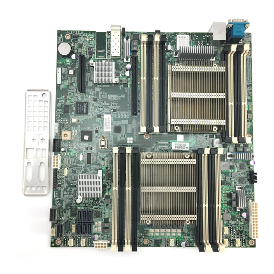
1.3 Product Features This chapter provides the detailed features for processor, chipset, and system memory, onboard LAN, VGA, I/O and PCI-E with pictures for your reference. Figure 1-1 Motherboard Overview B800G2 MLB has five kinds of SKU. Each system can be identified through SKU_ID configuration. -
Page 20: Table 1-3 Product Features
Table 1-3 Product Features Processor Dual Processors Intel® Xeon E5-2600 Chipset Intel C600 Patsburg-A or Patsburg-D System Memory 16x DDR3 DIMM slots Two DIMMs per channel Four DDR3 channels per CPU Onboard Storage Use PCH SCU Controllers BIOS ROM... -
Page 21: Boards Layout
1.4 Boards Layout The layout of mother board is shown as below. Each connector and major component is identified by number. Figure 1-2 Connectors and Component Locations of Motherboard Table 1-4 Connectors and Component Locations of Motherboard DIMM slots (J13, J14, J15, J16) Power Management connector (J98) Power Connector (J89) - Page 22 Fan connectors (J114, J115, J116, J117, J118, J119) [J115,J117,J119 are optional] DIMM slots (J1, J2, J3, J4) Fan connector (J113) [Optional] Fan connector (J112) CPU 0 (U4) DIMM slots (J5, J6, J7, J8) P12VA Power connector (J88) SATA connectors (J40, J41, J42, J43, J44, J45) FAN connectors (J107, J108, J109, J110, J111) [J107,J109,J111 are optional] SGPIO connector (J46)
- Page 23 PCI-E Slot 6 X 16 (J64) DIMM slots (J9, J10, J11, J12) UID BTN / LED (CR42) CPU 1 (U1) Gbe NIC1 / 2 (up/down) ports (J21) [for Gbe SKU] Dedicate NIC(up) and Rear USB(down) (J95) COM(up) / VGA(down) connector (J92)
-
Page 24: System Led And Button Information
1.5 System LED and Button Information 1.5.1 LED and Button Information of Motherboard Rear LED information of motherboard rear displays details regarding the NIC LEDs. Each NIC port contains two LEDs that show the status of network activity, link or speed. Figure 1-3 LEDs of Motherboard Rear Dedicate NIC Link LED Dedicate NIC Activity LED... - Page 25 LAN link / No access Green Blink LAN link / Access Link / Activity Green No connection Gbe NIC1 Linked to the network at 100Mbps Green Linked to the network at 1Gbps Gbe Speed Amber Linked to the network at 10Mbps LAN link / No access Green Blink...
- Page 26 Chapter 2 Hardware Operations Before You Start Screw Holes System Battery Processor System Memory System Configuration Jumpers...
-
Page 27: Hardware Operations
Hardware Operations 2 Hardware Operations This chapter provides the detailed information and replacement steps for motherboard, including system battery, processor, system memory, and system configuration jumper. The components shown in this chapter are mainly for your reference. Please take the actual shipment as standard. All descriptions in this chapter are based on one motherboard except special statement. -
Page 28: Screw Holes
Hardware Operations 2.2 Screw Holes 2.2.1 Motherboard Screw Holes The motherboard is designed with totally nine screw holes as the picture shows. Figure 2-1 Screws Placement of Motherboards Screw Hole Do not overly tighten the screws. Doing so may damage the motherboard. - Page 29 Hardware Operations...
-
Page 30: System Battery
Hardware Operations 2.3 System Battery The location of system battery is shown below: Figure 2-2 System Battery Location... -
Page 31: To Remove And Install The System Battery
Hardware Operations 2.3.1 To remove and install the system battery Release the battery form its holder by squeezing the metal clamp that extends above one edge of the battery. Lift the system battery up. To install the system battery, slide one edge of the battery under the holder’s lip with the positive side up. -
Page 32: Processor
Hardware Operations 2.4 Processor ® This motherboard supports one Intel Sandy Bridge-DT processor. Below set removing and installing heat sink and processor of motherboard. The location of processors on the motherboard is shown below: Figure 2-2 Location of Processors Processor... -
Page 33: To Remove The Heat Sink
Hardware Operations 2.4.1 To remove the heat sink Loosen four securing screws. Lift the heat sink up from the installed processor. Figure 2-3 Remove Heat Sink 2.4.2 To install the heat sink Reverse the steps above to install the heat sink. Before you put the heat sink on top of the installed processor, please do not forget to check if the grease is complete on bottom of the heat sink. -
Page 34: To Remove The Processor
Hardware Operations 2.4.3 To remove the processor Unlock the load lever and lift it up. Open the load plate. Figure 2-4 Opening the Load Plate Lift the processor out of the socket. Figure 2-5 Lifting the Processor out of the Socket... -
Page 35: To Install The Processor
Hardware Operations Close the load plate. Lock the load lever. Figure 2-6 Closing the Load Plate 2.4.4 To install the processor Reverse the steps above to install the processor. However, when inserting the processor into the socket, make sure that the golden corner on the processor is pointed toward the socket as picture shows: Figure 2-7 Pointing the Golden Corner toward the Socket When the processor is in place, press it firmly on the socket while you push down... - Page 36 Hardware Operations socket to avoid bending the pins and damaging the processor. If the processor does not fit completely, check its orientation or check for bent pins.
-
Page 37: System Memory
Hardware Operations 2.5 System Memory The motherboard supports 16 DDR3 DIMM slots, including Registered DIMMs (RDIMM), Load Reduced DIMMs (LRDIMM) and Unbuffered DIMMs (UDIMM). There are four DIMM channels per CPU, and 2 DIMM slots per channel. Data transfer rates can support DDR3 800/1066/1333/1600. -
Page 38: Figure 2-9 Dimm Socket Location
Hardware Operations Figure 2-9 DIMM Socket Location... -
Page 39: System Memory Organization Modes
Hardware Operations 2.5.1 System Memory Organization Modes The Romley-EP/EP 4S platform supports four different memory RAS modes: Independent Channel Mode, Rank Sparing Mode, Mirrored Channel Mode, and Lockstep Channel Mode. The rules on channel population and channel matching vary by the RAS mode used. - Page 40 Hardware Operations Channel 0 and Channel 1, and Channel 2 and Channel 3 must be populated identically with regards to size and organization. DIMM slot populations within a channel do not have to be identical but the same DIMM slot location across Channel 0 and Channel 1 and across Channel 2 and Channel 3 must be populated the same.
-
Page 41: Dimm Population Rule
Hardware Operations 2.5.2 DIMM Population Rule For two slots per channel configurations, the Romley-EP platform requires DIMMs within a channel to be populated starting with the DIMMs farthest from the processor in a “fill-farthest” approach. In addition, when populating a Quad-rank DIMM with a Single- or Dual-rank DIMM in the same channel, the Quad-rank DIMM must be populated farthest from the processor. - Page 42 Hardware Operations DDR3 RDIMM Population: DDR3 UDIMM Population: DDR3 LRDIMM Population:...
- Page 43 Hardware Operations DDR3L RDIMM Population (1.35V): DDR3L UDIMM Population (1.35V):...
- Page 44 Hardware Operations...
-
Page 45: To Remove A Dimm
Hardware Operations 2.5.2 To remove a DIMM Unlock a DIMM socket by pressing the retaining clips outward. This action releases the module and partially lifts it out of the socket. Lift out the DIMM. Figure 2-12 Lifting the DIMM out of the Socket 2.5.3 To install a DIMM Unlock a DIMM socket by pressing the retaining clips outward. - Page 46 Hardware Operations Figure 2-14 Inserting the DIMM into the Socket DIMMs fit in only one direction. DO NOT force a DIMM into the socket to avoid damaging the DIMM.
-
Page 47: System Configuration Jumpers
Hardware Operations 2.6 System Configuration Jumpers The motherboard involves one function jumper. The jumper is divided into seven pin groups. Figure 2-15 Location of Function Jumpers Table 2-1 Function of Function Jumpers Jumper Function BIOS Recovery Jumper Intruder header BIOS CMOS Clear Password Clear... - Page 48 Chapter 3 Connectors, Jumpers and Switches Mini SAS Connectors Power Management Connector Front Panel connector Power Connector Front USB Connector Fan Connectors PCI-E Slots P12V Power Connector SFP Connectors SATA Connectors NIC LAN and USB Ports SGPIO Connector COM and VGA Ports...
-
Page 49: Connectors, Jumpers And Switches
3 Connectors, Jumpers and Switches The locations of all the connectors described in this chapter are shown in “1.4 Connectors and Component Locations”. “Key” stands for foolproof feature; “NC” stands for unused. 3.1 Power Management Connector (J98) Figure 3-1 Power Management Connector Table 3-1 Pin Definition of Power Management Connector (J98) Signal Name I2C_PSU_SCL... -
Page 50: Power Connector (J89)
3.2 Power connector (J89) Figure 3-2 Power Connector Table 3-2 Pin Definition of Power Connector (J89) Signal Name Signal Name P3V3 P3V3 P3V3 N12V Ground Ground PS_EN_PSU_N Ground Ground Ground Ground Ground PGD_PSU_PWROK_5V P5V_AUX P12V P12V P3V3 Ground... -
Page 51: Fan Connectors (J106, J107, J108, J109, J110, J111, J112, J113, J114, J115, J116, J117, J118, J119)
3.3 Fan Connectors (J106, J107, J108, J109, J110, J111, J112, J113, J114, J115, J116, J117, J118, J119) Figure 3-3 Fan Connector Table 3-3 Pin Definition of Fan Connector (J106) Signal Name BMC_FAN_PWM_1_R BMC_FAN_TACH_1_R P12VA Ground Table 3-4 Pin Definition of Fan Connector (J107) [Optional] Signal Name BMC_FAN_PWM_8_R BMC_FAN_TACH_8_R... -
Page 52: Table 3-7 Pin Definition Of Fan Connector (J110)
Signal Name BMC_FAN_PWM_9_R BMC_FAN_TACH_9_R P12VA Ground Table 3-7 Pin Definition of Fan Connector (J110) Signal Name BMC_FAN_PWM_3_R BMC_FAN_TACH_3_R P12VA Ground Table 3-8 Pin Definition of Fan Connector (J111) [Optional] Signal Name BMC_FAN_PWM_10_R BMC_FAN_TACH_10_R P12VA Ground Table 3-9 Pin Definition of Fan Connector (J112) Signal Name BMC_FAN_PWM_4_R BMC_FAN_TACH_4_R... -
Page 53: Table 3-10 Pin Definition Of Fan Connector (J113) [Optional]
Table 3-10 Pin Definition of Fan Connector (J113) [Optional] Signal Name BMC_FAN_PWM_11_R BMC_FAN_TACH_11_R P12VA Ground Table 3-11 Pin Definition of Fan Connector (J114) Signal Name BMC_FAN_PWM_5_R BMC_FAN_TACH_5_R P12VA Ground Table 3-12 Pin Definition of Fan Connector (J115) [Optional] Signal Name BMC_FAN_PWM_12_R BMC_FAN_TACH_12_R P12VA... -
Page 54: Table 3-16 Pin Definition Of Fan Connector (J119) [Optional]
Signal Name P12VA Ground Table 3-16 Pin Definition of Fan Connector (J119) [Optional] Signal Name BMC_FAN_PWM_14_R BMC_FAN_TACH_14_R P12VA Ground... -
Page 55: P12V Power Connector (J88, J20)
3.4 P12V Power Connector (J88, J20) Figure 3-4 P12VB Power Connector Table 3-17 Pin Definition of P12VA Power Connector (J88) Signal Name Signal Name Ground P12VA Ground P12VA Ground P12VA Ground P12VA Table 3-18 Pin Definition of P12VB Power Connector (J20) Signal Name Signal Name Ground... -
Page 56: Sata Connectors (J40, J41, J42, J43, J44, J45)
3.5 SATA Connectors (J40, J41, J42, J43, J44, J45) Figure 3-5 SATA Connectors Table 3-19 Pin Definition of SATA Connectors (J40) Signal Name Ground SATA_TX1_C_DP SATA_TX1_C_DN Ground SATA_RX1_C_DN SATA_RX1_C_DP Ground Ground Ground Table 3-20 Pin Definition of SATA Connectors (J41) Signal Name Ground SATA_TX0_C_DP... -
Page 57: Table 3-21 Pin Definition Of Sata Connectors (J42)
Table 3-21 Pin Definition of SATA Connectors (J42) Signal Name Ground SATA_TX3_C_DP SATA_TX3_C_DN Ground SATA_RX3_C_DN SATA_RX3_C_DP Ground Ground Ground Table 3-22 Pin Definition of SATA Connectors (J43) Signal Name Ground SATA_TX2_C_DP SATA_TX2_C_DN Ground SATA_RX2_C_DN SATA_RX2_C_DP Ground Ground Ground... -
Page 58: Table 3-23 Pin Definition Of Sata Connectors (J44)
Table 3-23 Pin Definition of SATA Connectors (J44) Signal Name Ground SATA_TX5_C_DP SATA_TX5_C_DN Ground SATA_RX5_C_DN SATA_RX5_C_DP Ground Ground Ground Table 3-24 Pin Definition of SATA Connectors (J45) Signal Name Ground SATA_TX4_C_DP SATA_TX4_C_DN Ground SATA_RX4_C_DN SATA_RX4_C_DP Ground Ground Ground... -
Page 59: Sgpio Connector (J46)
3.6 SGPIO Connector (J46) Figure 3-6 SGPIO Connector Table 3-25 Pin Definition of SGPIO Connector (J46) Signal Name SGPIO_SATA_CLK SGPIO_SATA_LOAD SGPIO_SATA_DOUT0 SGPIO_SATA_DOUT1... -
Page 60: Mini Sas Connectors (J104, J105)
3.7 Mini SAS Connectors (J104, J105) Figure 3-7 Mini SAS Connectors Table 3-26 Pin Definition of Mini SAS Connectors (J104) Signal Name Signal Name SAS_PCH_TX_C_DP<3> SAS_PCH_RX_C_DP<3> SAS_PCH_TX_C_DN<3> SAS_PCH_RX_C_DP<3> SAS_PCH_TX_C_DP<2> SAS_PCH_RX_C_DP<2> SAS_PCH_TX_C_DN<2> SAS_PCH_RX_C_DP<2> SAS_PCH_TX_C_DP<1> SAS_PCH_RX_C_DP<1> SAS_PCH_TX_C_DN<1> SAS_PCH_RX_C_DP<1> SAS_PCH_TX_C_DP<0> SAS_PCH_RX_C_DP<0> SAS_PCH_TX_C_DN<0> SAS_PCH_RX_C_DP<0> TP_PCH_SAS1_SIDEBAND6 B11 SGPIO_SAS1_DATAIN_F Ground... -
Page 61: Table 3-27 Pin Definition Of Mini Sas Connectors (J105) [For Patsburg-D Sku]
Signal Name Signal Name Ground Ground Table 3-27 Pin Definition of Mini SAS Connectors (J105) [for Patsburg–D SKU] Signal Name Signal Name SAS_PCH_TX_C_DP<7> SAS_PCH_RX_C_DP<7> SAS_PCH_TX_C_DN<7> SAS_PCH_RX_C_DN<7> SAS_PCH_TX_C_DP<6> SAS_PCH_RX_C_DP<6> SAS_PCH_TX_C_DN<6> SAS_PCH_RX_C_DN<6> SAS_PCH_TX_C_DP<5> SAS_PCH_RX_C_DP<5> SAS_PCH_TX_C_DN<5> SAS_PCH_RX_C_DN<5> SAS_PCH_TX_C_DP<4> SAS_PCH_RX_C_DP<4> SAS_PCH_TX_C_DN<4> SAS_PCH_RX_C_DN<4> TP_PCH_SAS2_SIDEBAND6 B11 SGPIO_SAS2_DATAIN_F Ground SGPIO_SAS2_DATAOUT_F... -
Page 62: Front Panel Connector (J90)
3.8 Front Panel Connector (J90) Figure 3-8 Front Panel Connector Table 3-28 Pin Definition of Front Panel Connector (J90) Signal Name Signal Name P3V3_STBY P3V3_STBY P5V_STBY LED_PWR_GRN_N BMC_UID_LED_R_N P3V3 FP_HLTH_GRN_LED_N LED_HDD_ACT_R_N FP_HLTH_RED_LED_N BTN_FP_PWR_N P3V3_STBY Ground LED_NIC1_LINK_ACT_R_N BTN_FP_RST_N I2C_SDA_SENS_FP_BUF Ground I2C_SCL_SENS_FP_BUF BTN_UID_N INTRUDER_N LED_PWR_AMBER_R_N 21... -
Page 63: Front Usb Connector (J17)
3.9 Front USB Connector (J17) Figure 3-9 Front USB Connector Table 3-29 Pin Definition of Front USB Connector (J17) Signal Name Signal Name P5V_USB89 P5V_USB89 USB8_SB_L_DN USB9_SB_L_DN USB8_SB_L_DP USB9_SB_L_DP Ground Ground... -
Page 64: Pci-E Slots (J64, J80)
3.10 PCI-E Slots (J64, J80) There are four kinds of PCI-E slot on the motherboard. They are shown as below: 3.10.1 PCI-Ex16 Slot (J64) Figure 3-10 PCI-Ex16 Slot Table 3-30 Pin Definition of PCI-Ex16 Slot (J64) Signal Name Signal Name P12VB P3V3 P12VB... -
Page 65: Pci-Ex8 Slot (J80)
Signal Name Signal Name Ground Ground Ground Ground Ground Ground Ground Ground Ground Ground Ground Ground Ground Ground Ground Ground Ground Ground Ground Ground Ground Ground Ground Ground Ground Ground Ground Ground Ground Ground Ground Ground Ground Ground Ground Ground Ground Ground Ground... - Page 66 Signal Name Signal Name PE3_CPU0_SLOT2_TX_DP<7..0> PE3_CPU0_SLOT2_RX_DP<7..0> PE3_CPU0_SLOT2_TX_DP<7..0> PE3_CPU0_SLOT2_RX_DP<7..0> PE3_CPU0_SLOT2_TX_DP<7..0> PE3_CPU0_SLOT2_RX_DP<7..0> PE3_CPU0_SLOT2_TX_DP<7..0> PE3_CPU0_SLOT2_RX_DP<7..0> PE3_CPU0_SLOT2_TX_DP<7..0> PE3_CPU0_SLOT2_RX_DP<7..0> PE3_CPU0_SLOT2_TX_DP<7..0> PE3_CPU0_SLOT2_RX_DP<7..0> PE3_CPU0_SLOT2_TX_DP<7..0> PE3_CPU0_SLOT2_RX_DP<7..0> PE3_CPU0_SLOT2_TX_DP<7..0> PE3_CPU0_SLOT2_RX_DP<7..0> PE3_CPU0_SLOT2_TX_DN<7..0> PE3_CPU0_SLOT2_RX_DN<7..0> PE3_CPU0_SLOT2_TX_DN<7..0> PE3_CPU0_SLOT2_RX_DN<7..0> PE3_CPU0_SLOT2_TX_DN<7..0> PE3_CPU0_SLOT2_RX_DN<7..0> PE3_CPU0_SLOT2_TX_DN<7..0> PE3_CPU0_SLOT2_RX_DN<7..0> PE3_CPU0_SLOT2_TX_DN<7..0> PE3_CPU0_SLOT2_RX_DN<7..0> PE3_CPU0_SLOT2_TX_DN<7..0> PE3_CPU0_SLOT2_RX_DN<7..0> PE3_CPU0_SLOT2_TX_DN<7..0> PE3_CPU0_SLOT2_RX_DN<7..0> PE3_CPU0_SLOT2_TX_DN<7..0> PE3_CPU0_SLOT2_RX_DN<7..0> CLK_100M_PM_SLOT2_DP Ground CLK_100M_PM_SLOT2_DN PE_SE_PRSNT_N RST_PERST0_N PE_SE_PRSNT_N IRQ_LVC3_WAKE_N...
-
Page 67: Sfp Connectors (J28, J29)
3.11 SFP Connectors (J28, J29) SFP connectors are for 10Gbe SKU and the J28 is optional. Figure 3-12 SFP Connectors Table 3-32 Pin Definition of SFP connector (J28) [Optional for 10Gbe SKU] Signal Name Signal Name Ground Ground NIANTIC_SPD1_7_TX_FAULT NIANTIC_TX_P1_L0_DN NIANTIC_SPD1_3_TX_DISABLE NIANTIC_TX_P1_L0_DP I2C_NIC_SDA_P1_R... - Page 68 Signal Name Signal Name NIANTIC_SPD0_0_RX_LOS NIANTIC_RX_P0_L0_DP NIANTIC_SPD0_6_RS0/1_SENSE NIANTIC_RX_P0_L0_DN Ground Ground...
-
Page 69: Nic Lan And Usb Ports (J95, J21)
3.12 NIC LAN and USB Ports (J95, J21) 3.12.1 Dedicate NIC and Rear USB Connector (J95) Figure 3-13 Dedicate NIC and Rear USB Connector Table 3-34 Pin Definition of Dedicate NIC and Rear USB Connector (J95) Signal Name P5V_USB1011 USB10_SB_L_DN USB10_SB_L_DP Ground P5V_USB1011... -
Page 70: Gbe Nic Lan Port (J21)
Signal Name LED_BCM5221_LINKUP_R_N P3V3_STBY LED_BCM5221_ACT_R_N P3V3_STBY 3.12.2 Gbe NIC LAN port (J21) Gbe NIC LAN port is for Gbe SKU. Figure 3-14 Gbe NIC Ports Table 3-35 Pin Definition of Gbe NIC Ports (J21) [for Gbe SKU] Signal Name NIC2_MDI_0_DN NIC2_MDI_0_DP NIC2_MDI_1_DN NIC2_MDI_1_DP... - Page 71 Signal Name NIC1_MDI_3_DN NIC1_MDI_3_DP P1VB_STBY Ground NIC2_1000M_ORG_N NIC2_100M_GRN_N NIC2_ACT_N NIC2_LINK_N NIC1_1000M_ORG_N NIC1_100M_ORG_N NIC1_ACT_N NIC1_LINK_N Ground Ground Ground Ground...
-
Page 72: Com And Vga Ports (J92)
3.13 COM and VGA Ports (J92) Figure 3-15 VGA and COM Ports Table 3-36 Pin Definition of COM (Up) Port (J92) Signal Name COM1_RES_DCD COM1_RES_RX_N COM1_RES_TX_N COM1_RES_DTR Ground COM1_RES_DSR COM1_RES_RTS COM1_RES_CTS COM1_RES_RI Table 3-37 Pin Definition of VGA (Down) Port (J92) Signal Name VGA_G0_RED_L VGA_G0_GREEN_L... - Page 73 Signal Name VGA_DDCDAT_R VGA_HSYNC_LSHFTR_L VGA_VSYNC_LSHFTR_L VGA_DDCCLK_R...
- Page 74 Chapter 4 BIOS Setup BIOS Setup Utility Utility and POST Code...
-
Page 75: Bios Setup
BIOS Setup 4 BIOS Setup This section describes the BIOS Setup Utility options. You can run BIOS Setup with or without an operating system being present. Onboard devices are configured with the BIOS Setup utility that is embedded in flash ROM. The configuration utilities allow you to modify the CMOS RAM and NVRAM. -
Page 76: Bios Setup Utility
BIOS Setup 4.1 BIOS Setup Utility Note: In following table, Settings with (*) are BIOS Setup Defaults. 4.1.1 Main Aptio Setup Utility –Copyright © 2010 American Megatrends, Inc. Advanced Boot Security Save&Exit Event Logs Server Mgmt Main BIOS Information Set the Data/Time, Use Tab to BIOS Vendor American Megatrends switch... -
Page 77: Advanced
BIOS Setup 4.1.2 Advanced Aptio Setup Utility –Copyright © 2010 American Megatrends, Inc. Advanced Boot Security Save&Exit Event Logs Server Mgmt Main Intel(R) VT-d [Disabled] Restore AC Power Loss [Power off] ▶ Trusted Computing ▶ CPU Configuration ▶ Runtime Error Logging ▶... - Page 78 BIOS Setup 4.1.2.1 Trusted Configuration Aptio Setup Utility –Copyright © 2010 American Megatrends, Inc. Advanced Configuration TPM SUPPORT [Enable] TPM State [Disabled] Pending operation [None] Current Status Information TPM Enabled Status: [Disabled] TPM Active Status: [Deactivated] →←: Select Screen TPM Owner Status: [UnOwned] ↑↓: Select Item Enter: Select...
-
Page 79: Cpu Configuration
BIOS Setup 4.1.2.2 CPU Configuration Aptio Setup Utility –Copyright © 2010 American Megatrends, Inc. Advanced CPU Configuration ▶ Socket 0 CPU Information Socket 1 Not Present CPU Speed XXXX MHz 64-bit Supported Hyper-threading [Enabled] Active Processor Cores [All] →←: Select Screen Limit CPUID Maximum [Disabled] ↑↓: Select Item... - Page 80 BIOS Setup [Disabled] Limit CPUID Maximum Disabled for Window XP [Enabled] XD can prevent certain classes of malicious buffer [Disabled] overflow attacks when combined with a supporting OS Execute Disable Bit (Windows Server 2003 SP1, Windows XP SP2, SuSE [Enabled] Linux 9.2, RedHat Enterprise 3 Update 3).
- Page 81 BIOS Setup L2 Cache xx kB x 6 +/-: Change Opt. L3 Cache xx kB F1: General Help F2: Previous Values F3: Optimized Defaults F4: Save & Exit ESC: Exit Version 2.02.1205. Copyright © 2010 American Megatrends, Inc.
-
Page 82: Cpu Power Management Configuration
BIOS Setup 4.1.2.2.2 CPU Power Management Configuration Aptio Setup Utility –Copyright © 2010 American Megatrends, Inc. Advanced CPU Power Management Configuration Max Freq Ratio Power Technology [Custom] EIST [Enabled] Turbo Mode [Disabled] P-STATE Coordination [HW_ALL] CPU C3 Report [Disabled] CPU C6 report [Enabled] CPU C7 report [Disalbed]... - Page 83 BIOS Setup [Disabled] CPU C3 Report Enable/Disable CPU C3(ACPI C2) report to OS [Enabled] [Disabled] CPU C6 report Enable/Disable CPU C6(ACPI C3) report to OS [Enabled] [Disabled] Enable/Disable CPU C7(ACPI C3) report CPU C7 report to OS [Enabled] Package C State Limit Package C State limit No Limit [Performance]...
-
Page 84: Qpi Configuration
BIOS Setup 4.1.2.2.3 QPI Configuration Aptio Setup Utility –Copyright © 2010 American Megatrends, Inc. Advanced Current QPI Link Speed Slow Current QPI Link Freq Unknown QPI Link Frequency Select [Auto] QPI Link1 [Enabled] →←: Select Screen ↑↓: Select Item Enter: Select +/-: Change Opt. -
Page 85: Runtime Error Logging
BIOS Setup 4.1.2.3 Runtime Error Logging Aptio Setup Utility –Copyright © 2010 American Megatrends, Inc. Advanced Runtime Error Logging Support [Enabled] Memory Corr. Error Threshold PCI Error Logging Support [Disabled] →←: Select Screen ↑↓: Select Item Enter: Select +/-: Change Opt. F1: General Help F2: Previous Values F3: Optimized Defaults... -
Page 86: Sata Configuration
BIOS Setup 4.1.2.4 SATA Configuration Aptio Setup Utility –Copyright © 2010 American Megatrends, Inc. Advanced SATA Configuration SATA Port0 Not present SATA Port1 Not present SATA Port2 Not present SATA Port3 Not present SATA Port4 Not present SATA Port5 Not present SATA Mode [AHCI Mode] →←: Select Screen... -
Page 87: Sas Configuration
BIOS Setup [Compatible] [Disabled] Serial-ATA Controller 1 (2) Enabled/disable serial ATA Controller 1 [Enhanced] Note: 1* The “Hot Plug” option is shown when “SATA Mode” is AHCI Mode or RAID Mode; 2* The “Serial-ATA Controller 0 and 1” is only shown when “SATA Mode” is IDE Mode; 4.1.2.4.1 SAS Configuration Aptio Setup Utility –Copyright ©... -
Page 88: Usb Configuration
BIOS Setup 4.1.2.5 USB Configuration Aptio Setup Utility –Copyright © 2010 American Megatrends, Inc. Advanced USB Configuration USB Devices: 1 Keyboard, 1 Mouse, 2 Hubs Legacy USB Support [Enabled] EHCI Hand-off [Disabled] Port 60/64 Emulation [Enabled] →←: Select Screen USB hardware delays and time-outs: ↑↓: Select Item USB transfer time-out [20 sec]... - Page 89 BIOS Setup [10 sec] [20 sec] [10 sec] [20 sec] USB mass storage device Start Unit command Device reset time-out time-out. [30 sec] [40 sec] Maximum time the device will take before it [Auto] properly reports itself to the Host Controller. 'Auto' Device power-up delay uses default value: for a Root port it is 100 ms, for [Manual]...
- Page 90 BIOS Setup 4.1.2.6 Runtime Memory Hole Setting Aptio Setup Utility –Copyright © 2010 American Megatrends, Inc. Advanced Runtime Memory Hole Switch [Enabled] →←: Select Screen ↑↓: Select Item Enter: Select +/-: Change Opt. F1: General Help F2: Previous Values F3: Optimized Defaults F4: Save &...
- Page 91 BIOS Setup 4.1.2.7 Info Report Configuration Aptio Setup Utility –Copyright © 2010 American Megatrends, Inc. Advanced Info Report Configuration Post Report Post Report [Enabled] Delay Time Error Message Report Info Error Message [Disabled] Summary Screen →←: Select Screen Summary Screen [Disabled] ↑↓: Select Item Enter: Select...
-
Page 92: Super Io Configuration
BIOS Setup 4.1.2.8 Super IO Configuration Aptio Setup Utility –Copyright © 2010 American Megatrends, Inc. Advanced Super IO Configuration Super IO Chip AST2300 Serial Port 0 (COMA) [Enabled] Device Settings IO=3F8h; IRQ=4; Serial Port 1(COMB) [Enabled] Device Settings IO=2F8h; IRQ=3; →←: Select Screen ↑↓: Select Item Enter: Select... - Page 93 BIOS Setup 4.1.2.9 PCI Express Settings Aptio Setup Utility –Copyright © 2010 American Megatrends, Inc. Advanced ASPM Support [Disabled] →←: Select Screen ↑↓: Select Item Enter: Select +/-: Change Opt. F1: General Help F2: Previous Values F3: Optimized Defaults F4: Save & Exit ESC: Exit Version 2.02.1205.
- Page 94 BIOS Setup 4.1.2.10 ME Subsystem Aptio Setup Utility –Copyright © 2010 American Megatrends, Inc. Advanced Intel ME Subsystem Configuration ME BIOS Interface Version ME Version 2.1.2.10 ME FW Status Value 0x1f0345 ME FW State SPS ME FW Active ME FW Operation State M0 without UMA ME FW Error Code No Error...
- Page 95 BIOS Setup 4.1.2.11 Memory Configuration Aptio Setup Utility –Copyright © 2010 American Megatrends, Inc. Advanced Memory Configuration Total Memory XXXX MB(DDR3 1333) Current Memory Mode Independent Current Memory Speed XXXX MHz Mirroring Not Possible Sparing Not Possible Memory Mode [Independent] Numa [Disabled] DDR Speed...
- Page 96 BIOS Setup [Force DDR3 1866] [Auto] [1 Way] Select different Channel Interleaving Channel Interleaving [2 Way] setting. [3 Way] [4 Way] [Auto] [1 Way] Rank Interleaving [2 Way] Select different rank Interleaving setting. [3 Way] [4 Way] [Disabled] Patrol Scrub Enable/Disable Patrol Scrub [Enabled] [Disabled]...
- Page 97 BIOS Setup 4.1.2.12 Onboard Device Configuration Aptio Setup Utility –Copyright © 2010 American Megatrends, Inc. Advanced Legacy OpROM Support Launch PXE OpROM [Enabled] Launch Storage OpROM [Disabled] Onboard Device Configuration Ethernet Controller [Enabled] LAN1 [Enabled] LAN2 [Enabled] →←: Select Screen ↑↓: Select Item Enter: Select +/-: Change Opt.
-
Page 98: Serial Port Console Redirection
BIOS Setup 4.1.2.13 Serial Port Console Redirection Aptio Setup Utility –Copyright © 2010 American Megatrends, Inc. Advanced COM0 Console Redirection [Disabled] ▶ Console Redirection Settings COM1 Console Redirection [Disabled] ▶ Console Redirection Settings →←: Select Screen ↑↓: Select Item Enter: Select +/-: Change Opt. -
Page 99: Console Redirection Settings
BIOS Setup 4.1.2.13.1 Console Redirection Settings Aptio Setup Utility –Copyright © 2010 American Megatrends, Inc. Advanced COM0 Console Redirection Settings Terminal Type [ANSI] Bits per second [115200] Data bits Parity [None] Stop Bits Flow Control [None] VT-UTF8 Combo Key Support [Enabled] →←: Select Screen Recorder Mode... - Page 100 BIOS Setup A parity bit can be sent with the data bits to detect [None] some transmission errors. Even: parity bit is 0 if the [Even] num of 1's in the data bits is even. Odd: parity bit is [Odd] Parity 0 if num of 1's in the data bits is odd.
-
Page 101: Boot
BIOS Setup 4.1.3 Boot Aptio Setup Utility –Copyright © 2010 American Megatrends, Inc. Advanced Boot Security Save&Exit Event Logs Server Mgmt Main Boot Configuration Setup Prompt Timeout Bootup NumLock State [On] Quiet Boot [Disabled] CSM16 Module Version xx.xx GateA20 Active [Upon Request] Option ROM Message [Force BIOS]... - Page 102 BIOS Setup [Enabled] UPON REQUEST - GA20 can be disabled [Upon Request] using BIOS services. ALWAYS - do not GateA20 Active allow disabling GA20; this option is useful [Always] when any RT code is executed above 1MB. [Force BIOS] Option ROM Message Set display mode for Option ROM [Keep Current] [Disabled]...
- Page 103 BIOS Setup Aptio Setup Utility –Copyright © 2010 American Megatrends, Inc. Boot Set the system boot order Boot Option #1 [xxxxxxxxxxxxx] Boot Option #2 [xxxxxxxxxxxxx] Boot Option #3 [xxxxxxxxxxxxx] Boot Option #4 [xxxxxxxxxxxxx] →←: Select Screen ↑↓: Select Item Enter: Select +/-: Change Opt.
-
Page 104: Security
BIOS Setup 4.1.4 Security Aptio Setup Utility –Copyright © 2010 American Megatrends, Inc. Advanced Boot Security Save&Exit Event Logs Server Mgmt Main Password Description Setup Administrator Password If ONLY the Administrator's password is set, then this only limits access to Setup and is only asked for when entering Setup. -
Page 105: Save&Exit
BIOS Setup 4.1.5 Save&Exit Aptio Setup Utility –Copyright © 2010 American Megatrends, Inc. Advanced Boot Security Save&Exit Event Logs Server Mgmt Main Save Changes and Exit Discard Changes and Exit Save Changes and Reset Discard Changes and Reset Save Option Save Changes Discard Changes →←: Select Screen... -
Page 106: Event Logs
BIOS Setup Save the changes done so far as User Save as User Defaults Defaults. Restore the User Defaults to all the setup Restore User Defaults options. Boot Override Choose Boot Path 4.1.6 Event Logs Aptio Setup Utility –Copyright © 2010 American Megatrends, Inc. Advanced Boot Security Save&Exit... -
Page 107: Server Mgmt
BIOS Setup 4.1.7 Server Mgmt Aptio Setup Utility –Copyright © 2010 American Megatrends, Inc. Advanced Boot Security Save&Exit Event Logs Server Mgmt Main FRB-2 Timer [Enabled] FRB-2 Timer timeout [6 minutes] FRB-2 Timer Policy [Reset] ▶ System Event Log ▶ View FRU information ▶... - Page 108 BIOS Setup 4.1.7.1 System Event Log Aptio Setup Utility –Copyright © 2010 American Megatrends, Inc. Server Mgmt Enabling/Disabling Options Erasing Settings Erase SEL [No] When SEL is Full [Do Nothing] Custom EFI Logging Options Log EFI Status Codes [Both] NOTE: All values changed here do not →←: Select Screen take effect until computer is ↑↓: Select Item...
- Page 109 BIOS Setup 4.1.7.2 View FRU information Aptio Setup Utility –Copyright © 2010 American Megatrends, Inc. Server Mgmt FRU Information System Manufacturer xxxxxx System Product Name xxxxxx System Version xxxxxx System Serial Number xxxxxx Board Manufacturer xxxxxx Board Product Name xxxxxx Board Version xxxxxx Board Serial Number...
-
Page 110: Bmc Network Configuration
BIOS Setup 4.1.7.3 BMC network configuration Aptio Setup Utility –Copyright © 2010 American Megatrends, Inc. Server Mgmt BMC network configuration Lan channel 1 Configuration Address source [Unspecified] Station IP address xxx.xxx.xxx.xxx Subnet mask xxx.xxx.xxx.xxx Station MAC address xx-xx-xx-xx-xx-xx Router IP address xxx.xxx.xxx.xxx Router MAC address xx-xx-xx-xx-xx-xx... -
Page 111: Utility And Post Code
BIOS Setup 4.2 Utility and POST Code 4.2.1 BIOS Requirements Table 4-1 BIOS Requirements Description Utilities File Name Description Flash BIOS Image AFUDOS.EXE Under DOS ROM image file AMIBIOS Flash Utility & ROM image FB.BAT FBB.BAT Recovery Mode AMIBOOT.ROM ROM image 4.2.2 Rom Flash 4.2.2.1 Update under DOS prompt:... - Page 112 Appendix China RoHS Regulations...
-
Page 113: Appendix China Rohs Regulations
Appendix Appendix China RoHS Regulations Appendix Figure I China RoHS Regulations...
Need help?
Do you have a question about the B800 and is the answer not in the manual?
Questions and answers