Table of Contents

Related Manuals for KD1JV Designs AT Sprint 3B

Summary of Contents for KD1JV Designs AT Sprint 3B
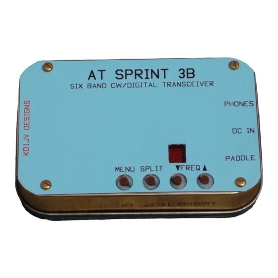
- Page 1 The AT Sprint 3B A very small, very effective, 6 band HF CW rig “DIGITAL READY” Operation and Assembly Manual for version 3B.1 By KD1JV Designs Steven Weber 633 Champlain St Berlin, NH 03570 kd1jv@moose.ncia.net http://kd1jv.qrpradio.com...
-
Page 2: Table Of Contents
Table of Contents Basic operation:...................................5 Turning the rig on and off:..............................5 Band selection and power up:.............................5 Control switches:................................5 Frequency tuning: .................................5 SPLIT MODES:................................6 Frequency annunciation while in Split modes:......................6 MENU:...................................6 Quick selections: ..............................6 DFE Mode: ................................6 Tune Mode: ................................7 Battery Voltage:................................7 MENU switch only selected functions:.........................7 Frequency readout: ..............................7 S: Selecting Keyer code speed;... - Page 3 Specifications: Frequency coverage: 80/40/30/20/17/15 meter bands Receiver MDS, 0.2 uV Small signal bandwidth 500 Hz Receive current, no signal 35 ma. Transmit power output: 2.5 watts at 9V, 4.5 watts at 12 V Transmit current: 460 ma at 9 V, 610 ma at 12 V Supply voltage: 5.5 volts minimum, 12 volts maximum...
-
Page 4: Basic Operation
Operation: Basic operation: Turning the rig on and off: As there is no power switch, the rig is turned on and off by inserting or removing the power plug from the jack. Make sure the plug is firmly and fully inserted into the jack. Try not to put any sideways pressure on the plug, it the jack may become intermittent. -
Page 5: Split Modes
Tuning limits: The tuning range includes the entire band, though SSB reception is not possible since it will be received on the wrong sideband. A double beep will sound when the band edges are reached and tuning will stop there, preventing out of band transmission. -
Page 6: Tune Mode
When four digits have been entered, the rig will re-tune to that frequency. If the frequency entered is beyond the tuning limits, DFE mode will simply terminate and the frequency will remain where it was. NOTE: DFE mode is not available if the rig is in Straight key mode. ●... -
Page 7: M: Keyer Memory Entry
gives a quick means of changing the code speed to more or less match another stations code speed during contests. Increase speed: Close RIGHT paddle or Tune Up switch. Decrease speed: Close the LEFT paddle or the Tune Down switch. NOTE: If the rig is in Straight key mode, the Tune up and Tune down switches are used to change code speed. -
Page 8: D: Digital Modes
Message 3 is sent by clicking the MENU switch within 1/2 of a second after releasing the Split switch. Message Pause, Stop and Beacon mode: After a message has started being transmitted, it maybe paused or stopped using the paddle. Pause: Closing the RIGHT paddle or Tune Up switch will pause the message for as long as the paddle is held closed. -
Page 9: A: Alternative Paddle
selections: (F will appear on the display) Frequency readout method: The method used for frequency readout maybe selected using these switches: SPLIT switch: Both Morse and display readout. Tune Up switch: Morse only readout. “MO” annunciated. Tune Down switch: LED Display only readout. “DO” annunciated. To store the preferences you have selected, click the MENU switch. - Page 10 very careful when using a fully charged gell cell to power the rig! Spare DC power plug: Mouser part number 171-3218-EX $1.22 Reprogramming the MPU. There is a row of pads above the MPU labeled “programmer”. These bring out the programming pins for the MPU, so that the firmware can be upgraded or changed.
-
Page 11: Assembly
Assembly: Your work area should be reasonably clean and uncluttered. Good lighting is a must. ● Empty the packets containing the parts into small paper bowls. This will ensure that they do not get lost. Some ● people like to do the assembly over a cookie sheet, as the lip around the edge helps to keep parts from going far. The metal sheet also provides some measure of static control, especially if you ground it. - Page 12 Using the parts placement guides: The parts placement guides on the following pages are color coded to show the location of the various parts. Parts which are not yet to be installed or already have been installed are colored the same as the background color. The guides are scaled so that the writing on them is easy to see on a computer monitor and come out crisper after the conversion to pdf.
-
Page 13: Reference Pictures Of The Front And Back Sides Of Completed Board
Reference pictures of the front and back sides of completed board:... -
Page 14: Overall Placement Diagrams
Overall placement diagrams. The front and back parts placement guides below should be printed out for convenient reference while building. Color coded locations match the colors of the corresponding part carrier. Part outlines with numbers inside indicate resistors and the resistor value to be placed there. Also refer to the photos of the completed board. -
Page 15: Parts Check List
Parts check list COLOR IS MARKER OR STICKER ON PART CARRIER PACKAGE VALUE/ SIZE MARKINGS OR COLOR VALUE MARKINGS OR COLOR 51 OHM 0805 270 OHMS 0805 22 p ORANGE 470 OHMS 0805 BROWN 2.2 K 0805 100 p PURPLE/Black stripe 3.6 K 0805 470 p... -
Page 16: Resistors
Resistors: Resistor locations are highlighted in yellow. Number shown in outline is the same as marked on body of part. When all the resistors have been installed (front and back), you will find there are five extras. These will be used on the filter module boards. - Page 17 Resistors Front side: 51 ohms 0805 10 K 0805 0805 13.7K 1% 1372 0805 0805 0805 0805 0805 47 K 0805 0805 100 K 0805 0805 Orange 10 uH 1206 0805 Yellow 0.15uH 1206 0805 L7: Orange sticker L4: Yellow sticker...
-
Page 18: Capacitors
Capacitors: Capacitors part carriers are color coded as the part its self has no markings to identify its value directly. Install all the capacitors of a given value (if required, both sides of the board) before starting to install another value. This will prevent mixing up values. -
Page 19: Semiconductors
Semiconductors: Little details you will need to know: Finding Pin 1. Some of the ICs used in this kit have a dot or indentation at the Pin 1 corner of the chip. For others, the Pin 1 locations isn't as obvious. The manufactures logo is sometimes used (as is the case for U1 and U2) or sometimes there is a line along the Pin 1 end of the chip. - Page 20 BACK SIDE U11: Green sticker, SLFJ (last two characters maybe different on actual part) D1: S2, larger black rectangle Note polarity! Faint line on one end of part faces line on board. D3 not installed at this time.
-
Page 21: Through Hole Parts
Through hole parts The SMT LED display should be soldered down first. Carefully note the end of the display which has the decimal point . Make sure that it is in the lower right corner, towards the switches, before soldering! Use a small tipped iron and try to make the solder wick up into the little solder cups on the display. -
Page 22: Filter Boards
Filter boards: First, separate the filter boards from the groups of three by snapping along the scored line. You should have five resistors (0805 size, each a different value) left over from the main board assembly. These will be used on the filter boards so that the processor can identify which module is for which band. -
Page 23: Check Out And Calibration
Check out and Calibration: Clean the board of any flux residue. This will help in inspecting all the solder connections. “Electrical Parts Cleaner”, available at most commercial electrical parts suppliers works well to remove flux. Denatured alcohol will also work. Avoid rubbing alcohol, as this leaves a white residue. -
Page 24: Local Oscillator Frequency Trim
10. The side tone will now announce “CO” A low pitched tone will be heard in the headphones. Local Oscillator frequency trim: This is used to trim the LO frequency to exactly match the center response of the IF crystal filter. This will ensure the best sensitivity of the receiver. - Page 25 though all kinds of weather. If it can stand up to this kind of abuse, it will defiantly stand up to typical daily use. A drill template as shown below is included on the CD located in the “front panel templates” file folder so that the various holes can be marked on the tin for drilling.
-
Page 26: Troubleshooting
Troubleshooting: Hopefully, your rig performed flawlessly during the above tests and calibration. Unfortunately, this is not always the case. Specific trouble shooting advice is hard to give, the best we can do is go over some basics. 99.99% of the time, the reason a kit does not work is due to soldering issues. Therefore, this is the first thing to look for. -
Page 27: Ic Voltage Tables: Receive Mode
IC Voltage tables: Receive mode 1.4V RFIN 5.0V 2.5V 5.0V 1.4V RFIN 4.3V 2.5V 2.5V 4.9V 2.5V 2.5V 3.9V 3.9V 2.5V U1/U2 SA612 mixer oscillator U3 LM4808 audio amp 2.2V Audio in P6 3.5V Control P1 5.0V 0.96V Audio out ---- ST in 2.2V Audio out... -
Page 28: Schematics
Schematics Receiver section schematic;... -
Page 30: Theory Of Operation
Theory of Operation: Controller: A Texas Instruments MSP430 micro controller (MPU) is used to control the rig. This is a 16 bit processor, with 8K of Flash memory, 256 bytes of RAM, two 64 byte “information” Flash memory locations, 23 I/O ports, and internal 8 MHz R/C clock oscillator. -
Page 31: Transmitter
The use of the MOSFET QSK switching greatly reduces or eliminates IMD problems which can be caused by a passive series L/C network with back to back limiting diodes at the L/C junction. This scheme is used in many QRP rigs, including the previous versions of this rig. -
Page 32: Digital Mode Operation
Digital mode operation: Before any digital mode can be used, you must build the digital interface shown below. The op amp must be a rail to rail output type which can operate at 3.5 volts, such as a ST microdevices TS-952. At the moment, kits are not available for this interface, but maybe at some time. -
Page 33: Calibration
bottom section is the transmitted text screen. If your using a PDA, when you activate the on screen keyboard, these windows will shrink so the keyboard is not covering up anything. Along the bottom of the screen are the menus. These are [Tools] [Channels] Macros] and [CAT] each has a pull up sub menu when selected. - Page 34 Now that the offset has been set, you can talk between your other rig and the ATS-3B. Try sending the macros and try different modulation modes. Using the CAT function. This function allows for setting the operating frequency of the rig. Selecting CAT then [Frequency] will bring up a numeric keypad.
Need help?
Do you have a question about the AT Sprint 3B and is the answer not in the manual?
Questions and answers