Table of Contents
Advertisement
Quick Links
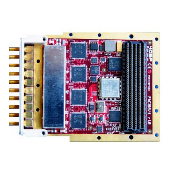
UM031 FMC168/4/2
r1.7
FMC168/4/2
User Manual
FMC168 / FMC164 / FMC162
Abaco Systems
Support Portal
This document is the property of Abaco Systems and may not be copied nor communicated to a
third party without the written permission Abaco Systems.
© Abaco Systems 2017
UM031
www.abaco.com
page 1 of 28
Advertisement
Table of Contents

Subscribe to Our Youtube Channel
Related Manuals for abaco systems FMC168

Summary of Contents for abaco systems FMC168
- Page 1 User Manual FMC168 / FMC164 / FMC162 Abaco Systems Support Portal This document is the property of Abaco Systems and may not be copied nor communicated to a third party without the written permission Abaco Systems. © Abaco Systems 2017 UM031 www.abaco.com...
- Page 2 UM031 FMC168/4/2 r1.7 Revision History Document Changes Author Peer Quality Date Review Approval Revision Release 2013/07/05 Added LPC compatibility 2013/07/25 Added FMC162, 2-channel 2014/03/18 variant Revised some descriptions 2014/04/07 and fixed typos. Correction main 2014/06/17 characteristics table. Corrected CPLD information...
-
Page 3: Table Of Contents
Onboard monitoring....................16 Environment ........................16 Temperature ......................16 Monitoring ......................16 Cooling ........................16 6.3.1 Convection cooling ..................17 6.3.2 Conduction cooling ..................17 Safety...........................17 EMC ..........................17 Ordering information ....................17 Warranty ........................17 Appendix A FMC168/4/2 connector pin-out – QDR mode ..........19 UM031 www.abaco.com page 3 of 28... - Page 4 UM031 FMC168/4/2 r1.7 Appendix B FMC168/4/2 connector pin-out – DDR mode ..........23 Appendix C CPLD Register map ...................27 UM031 www.abaco.com page 4 of 28...
-
Page 5: Acronyms And Related Documents
UM031 FMC168/4/2 r1.7 1 Acronyms and related documents 1.1 Acronyms Analog-to-Digital Converter Double Data Rate Digital Signal Processing EPROM Erasable Programmable Read-Only Memory FBGA Fineline Ball Grid Array FPGA Mezzanine Card FPGA Field Programmable Gate Array JTAG Join Test Action Group... -
Page 6: General Description
* HPC connections Figure 1: FMC168 block diagram Note1: Although the FMC168/4/2 is equipped with a HPC connector, it can be used in LPC carrier hardware. The LVDS interface on LPC runs at 500MHz DDR for 250Msps sampling rate. On HPC carriers the LVDS interface can be reduced to 250MHz DDR for 250Msps sampling. -
Page 7: Installation
Do not flex the card, and do not exceed the maximum torque specification on the SSMC connectors. • The FMC168/4/2 daughter card must be installed on a carrier card compliant to the FMC standard. • The FMC carrier card must support the low-pin count connector (160-pins) and may support the high-pin count connector (400-pins). - Page 8 The tables below provide the front label to A/D converter and FMC signal mappings. For the FMC168, the mapping is 1-to-1.For the reduced channel variants, the front panel labels don’t always match the FMC connector signal names. For example, data sampled from FMC162 input B is present on FMC connector CHC_D[3..0] (QDR mode).
-
Page 9: Electrical Specifications
Table 4: FMC162 Connector function assignment 4.2 Electrical specifications The FMC168/4/2 card is designed to operate in LVDS mode. The connections on FMC bank LA allow simultaneous sampling of eight (FMC168), four (FMC164), or two (FMC162) channels. This is referred to as QDR LVDS mode. With the use of the connections on FMC bank HA and HB, the digital interface rate can be reduced by a factor of two. -
Page 10: Jtag
4.2.5 JTAG The FMC168/4/2 has a CPLD device in the JTAG chain. The TDO pin of the CPLD is normally connected to the TDO pin of the top FMC connector through a buffer to ensure continuity of the JTAG chain. -
Page 11: Analog Input Channels
Table 5 : FMC168/4/2 daughter card main characteristics 4.4 Analog input channels The analog input signals are connected to the FMC168/4/2 via SSMC connectors on the front panel. Each channel can be assembled as an AC-coupled or DC-coupled input. Optionally, the FMC164/2 supports differential inputs using two connectors per channel. A 125MHz low-pass input filter can be assembled.. -
Page 12: External Clock Input
Note 2: When external clock is enabled, the onboard VCO might cause interference. The VCO cannot be powered down on the FMC168/4 r1.0. Please contact Abaco to have the onboard VCO disabled for external clock applications. - Page 13 UM031 FMC168/4/2 r1.7 reduce degradation of the data conversion performance. The user may choose to use an external sampling clock or an internal sampling clock. The AD9517 PLL and clock distribution device is the base of the clock tree. The external clock input is routed through RF switches and transformers that drive the reference input on the AD9517 (REFIN) and the primary clock input on the AD9517 (CLK).
-
Page 14: Pll Design
CLV1225A Figure 9: VCO loop filter design 4.9 Power supply Power is supplied to the FMC168/4/2 card through the FMC connector. The pin current rating is 2.7A, but the overall maximum is limited according to Table 6. Voltage # Pins... -
Page 15: Cpld
GA1. EEPROM address bit 1 connects to GA0. 5.1 CPLD The FMC168/4/2 has an onboard CPLD (XC2C256 CP132) used to control different devices on board. The CPLD communicates with the carrier hardware via an I C interface and acts as an I C-to-SPI bridge. -
Page 16: Onboard Monitoring
UM031 FMC168/4/2 r1.7 5.2 Onboard monitoring The FMC168/4/2 holds one AD7291 device for monitoring several power supply voltages and temperature on the board. The device can be programmed and read out through the I connection on the FMC connector. Parameter:... -
Page 17: Convection Cooling
6.3.1 Convection cooling The air flow provided by the fans of the chassis the FMC168/4/2 is enclosed in will dissipate the heat generated by the onboard components. A minimum airflow of 300 LFM is recommended. Optional Heat Sync Available, Contact sales and ask for Custom Option - C108. - Page 18 UM031 FMC168/4/2 r1.7 (optional) UM031 www.abaco.com page 18 of 28...
-
Page 19: Appendix Afmc168/4/2 Connector Pin-Out - Qdr Mode
UM031 FMC168/4/2 r1.7 Appendix A FMC168/4/2 connector pin-out – QDR mode AV57.1 LPC Pin Signal AV57.1 HPC Pin Signal AV57.1 HPC Pin Signal CLK0_M2C_N CLK_TO_FPGA_N HA00_N_CC CHA_FRM_N HB00_N_CC CHF_CLK_N CLK0_M2C_P CLK_TO_FPGA_P HA00_P_CC CHA_FRM_P HB00_P_CC CHF_CLK_P CLK1_M2C_N EXT_TRIGGER_N HA01_N_CC N.C. HB01_N N.C. - Page 20 I2C_SCL I2C_SCL DP9_C2M_N DP_C2M_N<9> I2C_SDA I2C_SDA DP9_C2M_P DP_C2M_P<9> PG_C2M PG_C2M DP9_M2C_N DP_M2C_N<9> DP9_M2C_P DP_M2C_P<9> Table 10: FMC168/4/2 - QDR MODE (yellow cells are N.C. on FMC164 and FMC162, blue cells are N.C. on FMC162) UM031 www.abaco.com page 20 of 28...
- Page 21 UM031 FMC168/4/2 r1.7 Signal Group Direction I/O Std Description CLK_TO_FPGA_P/N STATUS Output LVDS Spare clock output from AD9517 (OUT6). May be used for monitoring. EXT_TRIGGER_P/N TRIGGER Output LVDS Representation of the signal connected to the external trigger input. SYNC_FROM_FPGA_P/N SYNC...
- Page 22 N.A. Refer to section 4.2.2 GBTCLK1_M2C_P/N N.A. N.A. Refer to section 4.2.2 DP<0..9>_C2M_P/N N.A. N.A. Refer to section 4.2.2 DP<0..9>_M2C_P/N N.A. N.A. Refer to section 4.2.2 Table 11: Signal description FMC168/4/2 – QDR mode UM031 www.abaco.com page 22 of 28...
-
Page 23: Appendix B Fmc168/4/2 Connector Pin-Out – Ddr Mode
UM031 FMC168/4/2 r1.7 Appendix B FMC168/4/2 connector pin-out – DDR mode AV57.1 LPC Pin Signal AV57.1 HPC Pin Signal AV57.1 HPC Pin Signal CLK0_M2C_N CLK_TO_FPGA_N HA00_N_CC CHA_D12_N HB00_N_CC CHF_D6_N CLK0_M2C_P CLK_TO_FPGA_P HA00_P_CC CHA_D12_P HB00_P_CC CHF_D6_P CLK1_M2C_N EXT_TRIGGER_N HA01_N_CC CHA_D0_N HB01_N... - Page 24 DP9_C2M_N DP_C2M_N<9> PG_M2C PG_M2C DP9_C2M_P DP_C2M_P<9> I2C_SCL I2C_SCL DP9_M2C_N DP_M2C_N<9> I2C_SDA I2C_SDA DP9_M2C_P DP_M2C_P<9> Table 12: FMC168/4/2 - DDR MODE (yellow cells are N.C. on FMC164 and FMC162, blue cells are N.C. on FMC162) UM031 www.abaco.com page 24 of 28...
- Page 25 UM031 FMC168/4/2 r1.7 Signal Group Direction I/O Std Description CLK_TO_FPGA_P/N STATUS Output LVDS Spare clock output from AD9517 (OUT6). May be used for monitoring. EXT_TRIGGER_P/N TRIGGER Output LVDS Representation of the signal connected to the external trigger input. SYNC_FROM_FPGA_P/N SYNC...
- Page 26 Group Direction I/O Std Description GBTCLK1_M2C_P/N N.A. N.A. Refer to section 4.2.2 DP<0..9>_C2M_P/N N.A. N.A. Refer to section 4.2.2 DP<0..9>_M2C_P/N N.A. N.A. Refer to section 4.2.2 Table 13: Signal description FMC168/4/2 – DDR mode UM031 www.abaco.com page 26 of 28...
-
Page 27: Appendix C Cpld Register Map
UM031 FMC168/4/2 r1.7 Appendix C CPLD Register map Register Description 0x00 Command register (Write only, defaults to 0x00) Bit 0 Clock tree (AD9517) reset, This bit is self-clearing Bit 1 ADC (ADS42LB69) reset Bit 2..7 Reserved 0x01 Control register (Read/Write, defaults to 0x1D) Bit 0 VCO Enable (not available on r1.0 boards) - Page 28 UM031 FMC168/4/2 r1.7 to the selected device, outputting the 24-bit control word. Bit 7..0 x”01” for selecting AD9517 x”04” for selecting ADS42LB69 #0 (Channel A and C) x”08” for selecting ADS42LB69 #1 (Channel B and D) x”10” for selecting ADS42LB69 #2 (Channel E and G) x”20”...
Need help?
Do you have a question about the FMC168 and is the answer not in the manual?
Questions and answers