Table of Contents
Advertisement
Quick Links
Advertisement
Table of Contents

Summary of Contents for Artesyn ATCA-F140
- Page 1 ATCA-F140 Installation and Use P/N: 6806800M67R March 2017...
- Page 2 Artesyn reserves the right to revise this document and to make changes from time to time in the content hereof without obligation of Artesyn to notify any person of such revision or changes.
-
Page 3: Table Of Contents
2.9.2 Removing QSFP+ Transceiver Modules......... . 64 ATCA-F140 Installation and Use (6806800M67R) - Page 4 Base Channel Interface ............. . 96 ATCA-F140 Installation and Use (6806800M67R)
- Page 5 5.3.2 Configuring U-Boot to Boot from RAM Disk........117 ATCA-F140 Installation and Use (6806800M67R)
- Page 6 5.10 ATCA-F140-Specific U-Boot Environment Variables ........
- Page 7 Tested SFP+ Modules ............101 ATCA-F140 Installation and Use (6806800M67R)
- Page 8 Table 5-9 ATCA-F140 Specific U-Boot Environment Variables ....... .126 Table B-1 Artesyn Embedded Technologies - Embedded Computing Publications .
- Page 9 ATCA-F140 Block Diagram ........
- Page 10 List of Figures ATCA-F140 Installation and Use (6806800M67R)
-
Page 11: About This Manual
This document uses the following abbreviations: Abbreviation Description ATCA Advanced Telecom Computing Architecture Advanced Mezzanine Card BITS Building Integrated Timing Supply Base Interface Switch DDR3 Dual Data Rate 3 DIMM Dual In-line Memory Module DRAM Dynamic Random Access Memory ATCA-F140 Installation and Use (6806800M67R) - Page 12 Stacked Chip Scale Package SDRAM Synchronous Dynamic Random Access Memory Small Form Factor Pluggable SFP+ Small Form Factor Pluggable Plus SGMII Serial Gigabit Media Independent Interface Single Mode Fiber Service Processor Serial Present Detect Serial Peripheral Interface ATCA-F140 Installation and Use (6806800M67R)
- Page 13 File > Exit Notation for selecting a submenu <text> Notation for variables and keys [text] Notation for software buttons to click on the screen and parameter description Repeated item for example node 1, node 2, ..., node ATCA-F140 Installation and Use (6806800M67R)
- Page 14 Indicates a hazardous situation which, if not avoided, may result in minor or moderate injury Indicates a property damage message No danger encountered. Pay attention to important information ATCA-F140 Installation and Use (6806800M67R)
-
Page 15: Table
Added a new section Real Time Clock on page 114. 6806800M67K June 2014 Updated Chapter 6 Switches. 6806800M67J May 2014 Re-branded to Artesyn template and updated Table 4-6 on page 102. 6806800M67H November 2013 Updated Table 2-1 on page 6806800M67G... - Page 16 About this Manual About this Manual ATCA-F140 Installation and Use (6806800M67R)
-
Page 17: Safety Notes
Artesyn Embedded Technologies and our suppliers take significant steps to make sure that there are no bent pins on the backplane or connector damage to the boards prior to leaving the factory. - Page 18 (EMI) shielding to maintain EMC compliance. Board products are tested in a representative system to show compliance with the above mentioned requirements. A proper installation in a compliant system maintains the required performance. ATCA-F140 Installation and Use (6806800M67R)
- Page 19 Before installing or removing additional devices or modules, read the respective documentation and use appropriate tools. Blade Damage Incorrect installation of the blade can cause damage of the blade, Only use handles when installing/removing the blade to avoid damage/deformation to the faceplate and/or PCB. ATCA-F140 Installation and Use (6806800M67R)
- Page 20 Overheating and Blade Damage Operating the blade without forced air cooling may lead to overheating and thus damage of the blade. When operating the blade, make sure that forced air cooling is available in the shelf. ATCA-F140 Installation and Use (6806800M67R)
- Page 21 Setting/resetting the switches during operation can cause damage to the product. Check and change switch settings before you install the product. Product Damage Too much force may damage the reset switch. Use minimal force when pressing the reset switch. ATCA-F140 Installation and Use (6806800M67R)
- Page 22 Installing AMC modules with small operating temperature ranges into the ATCA-F140 may further restrict the operating temperature range of the ATCA-F140. Make sure that the operating temperature of any installed AMC modules and the ATCA-F140 as a bundle are within allowed limits...
- Page 23 SFP/SFP+/QSFP+ module inoperable. Only remove the optical plug when you are ready to connect a cable to the SFP/SFP+/QSFP+ module. When no cable is connected, cover the port with an optical port plug. ATCA-F140 Installation and Use (6806800M67R)
- Page 24 Do not use a screw driver to remove the battery from its holder. Environment Environmental Damage Improperly disposing of used products may harm the environment. Always dispose of used products according to your country’s legislation and manufacturer’s instructions. ATCA-F140 Installation and Use (6806800M67R)
-
Page 25: Sicherheitshinweise
Installieren Sie keine Ersatzteile oder führen Sie keine unerlaubten Veränderungen am System durch, sonst verfällt die Garantie. Wenden Sie sich für Wartung oder Reparatur bitte an die für Sie zuständige Geschäftsstelle von Artesyn Embedded Technologies. So stellen Sie sicher, dass alle sicherheitsrelevanten Aspekte beachtet werden. - Page 26 Sie sicher, dass ausreichend Schutz vor Störstrahlung vorhanden ist. Die Blades müssen mit der Frontblende installiert und alle freien Steckplätze müssen mit Blindblenden abgedeckt sein. Änderungen, die nicht ausdrücklich von Artesyn Embedded Technologies erlaubt sind, können Ihr Recht das System zu betreiben zunichte machen. ATCA-F140 Installation and Use (6806800M67R)
- Page 27 Beschädigung des Produktes und der Zusatzmodule Fehlerhafter Ein- oder Ausbau von Zusatzmodulen führt zu Beschädigung des Produktes oder der Zusatzmodule. Lesen Sie deshalb vor dem Ein- oder Ausbau von Zusatzmodulen die Dokumentation und benutzen Sie angemessenes Werkzeug. ATCA-F140 Installation and Use (6806800M67R)
- Page 28 Betreiben Sie das Blade nur innerhalb der angegebenen Grenzwerte für die relative Luftfeuchtigkeit und Temperatur. Stellen Sie vor dem Einschalten des Stroms sicher, dass sich auf dem Blade kein Kondensat befindet und betreiben Sie das Blade nicht unter -5°C. ATCA-F140 Installation and Use (6806800M67R)
- Page 29 Das Verstellen von Schaltern während des laufenden Betriebes kann zur Beschädigung des Produktes führen. Prüfen und ändern Sie die Schaltereinstellungen, bevor Sie das Produkt installieren. Beschädigung des Produktes Zu viel Druck kann den Reset Schalter beschädigen. Drücken Sie den Reset Schalter nur leicht. ATCA-F140 Installation and Use (6806800M67R)
- Page 30 Ein leerer AMC-Steckplatz kann zu verminderter Kühlung des Shelfs sowie starker elektromagnetischer Strahlung führen und somit eine Überschreitung von EMV-Grenzwerten zur Folge haben. Installieren Sie daher immer ein Filler-Panel in einen anderweitig nicht verwendeten AMCSteckplatz. ATCA-F140 Installation and Use (6806800M67R)
- Page 31 Bestimmungen für Laserprodukte eingehalten werden. Verletzungsgefahr der Augen Optische SFP/SFP+-Module können Laserstrahlen aussenden, wenn kein Kabel angeschlossen ist. Blicken Sie daher nicht direkt in die Öffnung eines SFP/SFP+-Moduls, um Verletzungen der Augen zu vermeiden. ATCA-F140 Installation and Use (6806800M67R)
- Page 32 Benutzen Sie keinesfalls einen Schraubendreher, um die Batterie aus der Halterung zu nehmen. Umweltschutz Umweltverschmutzung Falsche Entsorgung der Produkte schadet der Umwelt. Entsorgen Sie alte Produkte gemäß der in Ihrem Land gültigen Gesetzgebung und den Empfehlungen des Herstellers. ATCA-F140 Installation and Use (6806800M67R)
-
Page 33: Introduction
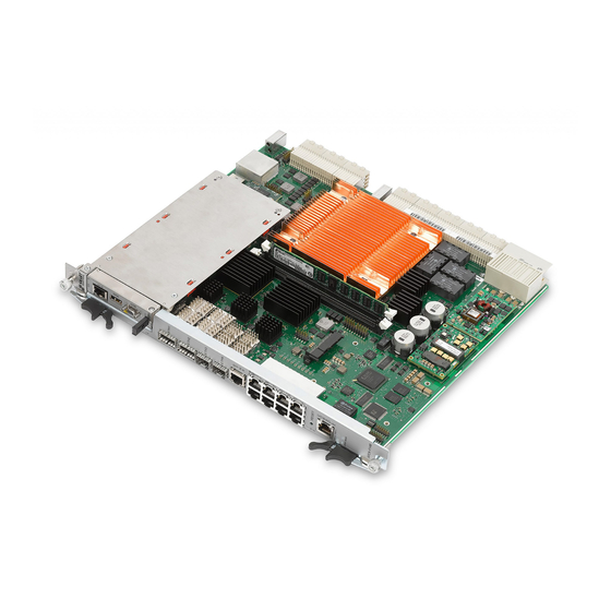
Introduction Features The ATCA-F140 is a hub board as defined in PICMG 3.0 Revision 3.0 Advanced TCA Base Specification and PICMG 3.1 Revision 1.0 Specification Ethernet/Fiber Channel for AdvancedTCA Systems. It supports several Base and Fabric Channel Ethernet interfaces to the Zone 2 backplane. -
Page 34: Table 1-1 Standard Compliances
ETSI public transportation requirement on system level Class 2.3 Telcordia GR-1089-CORE Electromagnetic Compatibility and Electrical Safety - Generic Criteria for Network Telecommunications Equipment Telcordia GR-63-CORE NEBS Requirements: Physical Protection Telcordia SR-3580 NEBS Criteria Level 3 ATCA-F140 Installation and Use (6806800M67R) -
Page 35: Mechanical Data
Introduction Table 1-1 Standard Compliances (continued) Standard Description EN55022 Class A (EU) EMC requirements (legal) on system level (predefined Artesyn Embedded Technologies system) EN 55024 (EU) FCC 47 CFR Part 15 Subpart B (US), Class A AS/NZS CISPR 22 Class A (Austra-... -
Page 36: Table 1-3 Blade Variants - Ordering Information
Ordering Information The following table lists the blade variants that were available as of the time of writing this manual. Consult your local Artesyn Embedded Technologies sales representative for the availability of further variants. Table 1-3 Blade Variants - Ordering Information... - Page 37 Introduction Table 1-4 Blade Accessories - Ordering Information (continued) Accessory Description HDD-500G-SATA Direct mount 500GB HDD for ATCA-F125 & ATCA-F140, high durability - SATA PRAMC-7311 AMC with INTEL COREI7 Processor, 4GB DDR3 - mid size SW-WR-PRAMC-7311 CD with WR PNE 3.0 and BBS for the PRAMC-7311, single blade license...
-
Page 38: Figure 1-1 Serial Number Location
Introduction Product Identification The following graphic shows the location of the serial number label. Figure 1-1 Serial Number Location Serial Number ASSY# COO LABEL PIN1 PIN1 ATCA-F140 Installation and Use (6806800M67R) -
Page 39: Hardware Preparation And Installation
Chapter 2 Hardware Preparation and Installation Overview This chapter provides the information that you need to install the ATCA-F140 and its accessories into your AdvancedTCA system. Removal procedures are also included. To install the blade, follow these steps: 1. Unpack and inspect the blade. -
Page 40: Requirements
Improper disposal of used products may harm the environment. Always dispose of used products according to your country’s legislation and manufac- turer’s instructions. Requirements This section shows the environmental and power requirements of the ATCA-F140 blade. ATCA-F140 Installation and Use (6806800M67R) -
Page 41: Table 2-1 Environmental Requirements
Operating temperatures refer to the temperature of the air circulating around the blade, and not to component temperatures. If you integrate the blade in your own non-Artesyn Embedded Technologies system, please contact your local sales representative for further safety information. -
Page 42: Thermal Requirements
100 mm unpackaged (according to Telcordia GR-63-core) 2.3.2 Thermal Requirements In order for the ATCA-F140 to cool properly when the operating temperature is at the maximum (55 C), the chassis must meet or exceed CP-TA B.3 ATCA Chassis Specification. CP- °... -
Page 43: Power Requirements
The following table show typical examples of the power requirements, with and without accessories installed. For information on the accessories' power requirements, refer to the documentation delivered together with the respective accessory or consult your local Artesyn Embedded Technologies representative for further details. -
Page 44: Table 2-2 Power Requirements
(without RTM-ATCA-F140) no AMC installed Rear Transition Modules If applicable, install a rear transition module. For more information, refer the RTM-ATCA-F140 Installation and Use manual. The RTMs are not hot-swappable. Before installation, make sure that no front blade is installed in its respective slot, or that the front blade is powered-down. -
Page 45: Blade Configuration
Setting/resetting the switches during operation can cause damage to the product. Check and change switch settings before installing the product. Product Damage Too much force may damage the reset switch. Use minimal force when pressing the reset switch. ATCA-F140 Installation and Use (6806800M67R) -
Page 46: Sata Drive Installation
2.5.1 SATA Drive Installation An optional SATA drive can be installed on the ATCA-F140. This is a 2.5 inch form factor drive, designed for extreme temperature and vibration environments and has been tested and approved for use on the ATCA-F140. The hard drive kits available at the time of release are listed in Table "Blade Accessories - Ordering Information"... -
Page 47: Installing The Blade
If there is a Rear Transition Module (RTM) to install, install and secure the RTM first as described in the RTM-ATCA-F140 Installation and Use Guide, then install the front blade. If an RTM is already installed, make sure that the RTM faceplate screws are fully tightened to secure the RTM to the shelf. - Page 48 Latch Handle 2. Slide the latch into the release position and pull out the handle outward to unlatch the handle from the faceplate. Do not pull the handle fully outward. ATCA-F140 Installation and Use (6806800M67R)
- Page 49 If your shelf is powered, as soon as the blade is connected to the backplane power pins, the blue LED is illuminated. ATCA-F140 Installation and Use (6806800M67R)
-
Page 50: Removing The Blade
ESD-safe environment. Damage of the blade Incorrect installation of the blade can cause damage of the blade. Only use handles when installing/removing the blade to avoid damage/deformation to the faceplate and/or PCB. ATCA-F140 Installation and Use (6806800M67R) - Page 51 If the LED continues to blink, it is possible that the upper layer software has rejected the blade extraction request. 3. Remove the faceplate cables, if applicable. 4. Remove the blade from the shelf. ATCA-F140 Installation and Use (6806800M67R)
-
Page 52: Amc Module Installation And Removal
Artesyn Embedded Technologies. Installing and operating other AMC modules may damage the AMC bay and the blade. Limitation of Operating Temperature Range Installing AMC modules with small operating temperature ranges into the ATCA-F140 may further restrict the operating temperature range of the ATCA-F140. - Page 53 LED. 1. Remove any cables that are connected to the AMC module faceplate connectors. 2. Gently pull the module latch outwards, approximately 3 mm away from its locked position. ATCA-F140 Installation and Use (6806800M67R)
- Page 54 4. Once the blue LED glows steadily, gently pull the AMC module handles outwards to disconnect the module from the AMC connectors. Continue to gently slide the module outwards along the guide rails. Install the filler panel. ATCA-F140 Installation and Use (6806800M67R)
-
Page 55: Installing And Removing Sfp Modules
The presence and also the type of SFP modules is automatically detected. The maximum power consumption of each SFP module should be 1W. The maximum power consumption of each SFP+ module should be 1.5W. ATCA-F140 Installation and Use (6806800M67R) -
Page 56: Installing An Sfp Module
1. Slide the SFP module into the slot until it locks into position. The SFP/SFP+ module will fully insert only if it is installed in the proper orientation. If it does not fully insert, rotate it 180 degrees and re-install. ATCA-F140 Installation and Use (6806800M67R) - Page 57 SFP module inoperable. Only remove the optical plug when you are ready to connect a cable to the SFP module. When no cable is connected, cover the port with an optical port plug. ATCA-F140 Installation and Use (6806800M67R)
- Page 58 Hardware Preparation and Installation 3. Connect the network cable to the SFP module ATCA-F140 Installation and Use (6806800M67R)
-
Page 59: Removing An Sfp Module
In order to remove an SFP module, proceed as follows. 1. Remove any connected cable from the SFP module. 2. Open the SFP latch. Note that the latch mechanism of your SFP module may be ATCA-F140 Installation and Use (6806800M67R) - Page 60 Hardware Preparation and Installation slightly different compared to the latch shown in the following figure. ATCA-F140 Installation and Use (6806800M67R)
- Page 61 SFP module inoperable. Only remove the optical plug when you are ready to connect a cable to the SFP module. When no cable is connected, cover the port with an optical port plug. ATCA-F140 Installation and Use (6806800M67R)
-
Page 62: Installing And Removing Qsfp+ Modules
When installing and using optical QSFP+ modules which are classified as laser products, make sure to comply to the respective regulations. The maximum power consumption of each QSFP+ module should be 2W. ATCA-F140 Installation and Use (6806800M67R) -
Page 63: Installing Qsfp+ Transceiver Modules
QSFP+ transceiver connects with the socket electrical connector. For QSFP+ transceivers with a bail-clasp latch, keep it aligned in a vertical position. For QSFP+ transceivers with a pull-tab, make sure that the identifier label is on top. ATCA-F140 Installation and Use (6806800M67R) -
Page 64: Removing Qsfp+ Transceiver Modules
Install the dust plug into the transceiver’ optical bore. Hold the tab and pull the receiver gently to release the transceiver from the socket. Slide the transceiver from the socket. Place the QSFP+ transceiver into an anti-static bag. ATCA-F140 Installation and Use (6806800M67R) -
Page 65: Figure 3-1 Atca-F140 Faceplate
Chapter 3 Controls, LEDs, and Connectors Faceplate This section describes the details of the ATCA-F140 faceplate LEDs. The following figure illustrates the faceplate view of the blade. Figure 3-1 ATCA-F140 Faceplate ARTESYN AMC Bay Out of Service LED In Service LED... -
Page 66: Leds
(Telco Clock LED 1) Green On - Master Clock Generator Blinking - Stand Alone Master Blinking - Status unknown LOCK Yellow On -Hold Over (Telco Clock LED 3) Blinking - Free Run Green Locked Blinking - Status unknown ATCA-F140 Installation and Use (6806800M67R) -
Page 67: Table 3-2 Service Processor Ethernet Rj45 Connector Pin Assignment (J9)
RJ45 Pin 10Base-T or 100Base-TX 1000Base-T ETH_TX+ ETH_DA+ ETH_TX- ETH_DA- ETH_RX+ ETH_DB+ ETH_DC+ ETH_DC- ETH_RX- ETH_DB- ETH_DD+ ETH_DD- Table 3-3 Service Processor Serial RS232 RJ45 Connector (J1) RJ45 Pin Function (RS232) Not used Not used ATCA-F140 Installation and Use (6806800M67R) -
Page 68: Table 3-4 Qsfp+ Connector Pin Assignment
Table 3-4 QSFP+ Connector Pin Assignment Contact Contact Number Function Number Function TX2n TX1n TX2p TX1p TX4n TX3n TX4p TX3p ModselL LPMode ResetL Vcc1 VccRx VccTx IntL ModPrsL RX3p RX4p RX3n RX4n RX1p RX2p RX1n RX2n ATCA-F140 Installation and Use (6806800M67R) -
Page 69: Table 3-5 Sfp+ Connector Pin Assignment
Table 3-5 SFP+ Connector Pin Assignment Contact Contact Number Function Number Function TX_FAULT TX_DISABLE I2C_SDA I2C_SCL VCCr (+3.3V) MOD_ABS VCCt (+3.3V) Table 3-6 Master/Slave Sync Connector (J12-U1) RJ45 Pin Function Transmit + Transmit - Receive + Receive - ATCA-F140 Installation and Use (6806800M67R) -
Page 70: Table 3-7 Inter-Shelf Connectors (J12-L1, L2, L3, U2, U3)
Port 3 - Port 2 - Port 4 + Port 4 - Table 3-8 T1/E1 Port Connectors (J12-L4 and J12-U4) RJ45 Pin Function RX Ring RX Tip TX Ring TX Tip Port 2 - Shield Shield ATCA-F140 Installation and Use (6806800M67R) -
Page 71: Table 3-9 Zone 1 Connector P10 Pin Assignment
IPMB Data Port A IPMB Clock Port B IPMB Data Port A 17 - 24 Not used Shelf Ground Logic Ground Enable B Voltage Return A Voltage Return B Early -48V A Early -48V B Enable A ATCA-F140 Installation and Use (6806800M67R) -
Page 72: Table 3-10 Connector J20 Pin Assignment
Column C Column D Column E Column F Column G Column H FIX_P11_TX2+ FIX_P11_TX2- FIX_P11_RX2+ FIX_P11_RX2- FIX_P11_TX3+ FIX_P11_TX3- FIX_P11_RX3+ FIX_P11_RX3- FIX_P11_TX0+ FIX_P11_TX0- FIX_P11_RX0+ FIX_P11_RX0- FIX_P11_TX1+ FIX_P11_TX1- FIX_P11_RX1+ FIX_P11_RX1- FIX_P10_TX2+ FIX_P10_TX2- FIX_P10_RX2+ FIX_P10_RX2- FIX_P10_TX3+ FIX_P10_TX3- FIX_P10_RX3+ FIX_P10_RX3- ATCA-F140 Installation and Use (6806800M67R) -
Page 73: Table 3-12 Connector J22 Pin Assignment
FIX_P4_TX0+ FIX_P4_TX0- FIX_P4_RX0+ FIX_P4_RX0- FIX_P4_TX1+ FIX_P4_TX1- FIX_P4_RX1+ FIX_P4_RX1- FIX_P3_TX2+ FIX_P3_TX2- FIX_P3_RX2+ FIX_P3_RX2- FIX_P3_TX3+ FIX_P3_TX3- FIX_P3_RX3+ FIX_P3_RX3- FIX_P3_TX0+ FIX_P3_TX0- FIX_P3_RX0+ FIX_P3_RX0- FIX_P3_TX1+ FIX_P3_TX1- FIX_P3_RX1+ FIX_P3_RX1- FIX_P2_TX2+ FIX_P2_TX2- FIX_P2_RX2+ FIX_P2_RX2- FIX_P2_TX3+ FIX_P2_TX3- FIX_P2_RX3+ FIX_P2_RX3- FIX_P2_TX0+ FIX_P2_TX0- FIX_P2_RX0+ FIX_P2_RX0- FIX_P2_TX1+ FIX_P2_TX1- FIX_P2_RX1+ FIX_P2_RX1- ATCA-F140 Installation and Use (6806800M67R) -
Page 74: Table 3-13 Connector J23 Pin Assignment
BIX_P12_DA+ BIX_P12_DA- BIX_P12_DB+ BIX_P12_DB- BIX_P12_DC+ BIX_P12_DC- BIX_P12_DD+ BIX_P12_DD- BIX_P13_DA+ BIX_P13_DA- BIX_P13_DB+ BIX_P13_DB- BIX_P13_DC+ BIX_P13_DC- BIX_P13_DD+ BIX_P13_DD- BIX_P14_DA+ BIX_P14_DA- BIX_P14_DB+ BIX_P14_DB- BIX_P14_DC+ BIX_P14_DC- BIX_P14_DD+ BIX_P14_DD- BIX_P15_DA+ BIX_P15_DA- BIX_P15_DB+ BIX_P15_DB- BIX_P15_DC+ BIX_P15_DC- BIX_P15_DD+ BIX_P15_DD- BIX_P16_DA+ BIX_P16_DA- BIX_P16_DB+ BIX_P16_DB- BIX_P16_DC+ BIX_P16_DC- BIX_P16_DD+ BIX_P16_DD- ATCA-F140 Installation and Use (6806800M67R) -
Page 75: Table 3-15 Connector J30 Pin Assignment
Column C Column D Column E Column F Column G Column H BIX_XG0_TX2+ BIX_XG0_TX2- BIX_XG0_RX2+ BIX_XG0_RX2- BIX_XG0_TX3+ BIX_XG0_TX3- BIX_XG0_RX3+ BIX_XG0_R BIX_XG0_TX0+ BIX_XG0_TX0- BIX_XG0_RX0+ BIX_XG0_RX0- BIX_XG0_TX1+ BIX_XG0_TX1- BIX_XG0_RX1+ BIX_XG0_R BIX_XG1_TX2+ BIX_XG1_TX2- BIX_XG1_RX2+ BIX_XG1_RX2- BIX_XG1_TX3+ BIX_XG1_TX3- BIX_XG1_RX3+ BIX_XG1_R ATCA-F140 Installation and Use (6806800M67R) -
Page 76: Table 3-17 Connector J32 Pin Assignment
Column G Column H FIX_P15_TX2+ FIX_P15_TX2- FIX_P15_RX2+ FIX_P15_RX2- FIX_P15_TX3+ FIX_P15_TX3- FIX_P15_RX3 FIX_P15_RX3 FIX_P15_TX0+ FIX_P15_TX0- FIX_P15_RX0+ FIX_P15_RX0- FIX_P15_TX1+ FIX_P15_TX1- FIX_P15_RX1 FIX_P15_RX1 FIX_P14_TX2+ FIX_P14_TX2- FIX_P14_RX2+ FIX_P14_RX2- FIX_P14_TX3+ FIX_P14_TX3- FIX_P14_RX3 FIX_P14_RX3 FIX_P14_TX0+ FIX_P14_TX0- FIX_P14_RX0+ FIX_P14_RX0- FIX_P14_TX1+ FIX_P14_TX1- FIX_P14_RX1 FIX_P14_RX1 ATCA-F140 Installation and Use (6806800M67R) - Page 77 Column B Column C Column D Column E Column F Column G Column H RTM_SCL RTM_SDA SPI_CS2_L RTM_RST_L RTM_SW_CLOS RTM_PWRGOOD BIX_P19_RTM BIX_P19_RTM ED_L _TX+ _TX- +12V_RTM +12V_RTM SPI_MISO SPI_MOSI SPI_SCK RTM_PS0_L BIX_P19_RTM BIX_P19_RTM _RX+ _RX- ATCA-F140 Installation and Use (6806800M67R)
-
Page 78: Figure 3-2 Module Connectors Locations
J8 AMC Connector P50 COP Header Battery ASSY# P15 H8S debug P9 H8S console COO LABEL J11 SATA Connector PIN1 PIN1 DIP Switch P17 SPI Flash Prog P12 JTAG Header J3 DIMM Socket J2 DIMM Socket ATCA-F140 Installation and Use (6806800M67R) -
Page 79: Table 3-18 Amc Bay Connector Pin Assignment
82571EB) AMC_TX0- PCIe_CLK+ Unused 148 Unused BIX_P18) AMC_RX4+ (to PCIe_CLK- Unused 149 GND 82571EB) AMC_RX0+ (to AMC_RX4- (to 150 Unused BIX_P18) 82571EB) AMC_RX0- PS0# Unused 151 Unused BIX_P18) AMC_TX5+ (to +12V Unused 152 GND 82571EB) ATCA-F140 Installation and Use (6806800M67R) - Page 80 167 TRST# 82571EB) RTM) AMC_RX2+ (to AMC_TX7- (to 100 AMC_RX10+ (to 168 TDO SATA mux) 82571EB) RTM) AMC_RX2- 101 GND TCLKC- 169 TDI SATA mux) AMC_RX7+ (to 102 AMC_TX10- (to TCLKC+ 170 GND 82571EB) RTM) ATCA-F140 Installation and Use (6806800M67R)
-
Page 81: Table 3-19 J2/J3 Memory Socket Pin Assignment
DQS1# 50 CKE0 DQS4 DQ30 DQ55 DQS1 +1.5V DQ31 +1.5V DQ34 RAS# DQ60 DQ10 ERROUT 88 DQ35 CS0# DQ61 DQ11 +1.5V +1.5V DQ40 ODT0 DQ16 DQ41 DQ17 +1.5V +1.5V DQS5# 128 DQ62 DQS2# 59 DQS5 DQ63 ATCA-F140 Installation and Use (6806800M67R) -
Page 82: Table 3-20 J11 Sas/Sata Connector Pin Assignment
The following table shows the pinout assignment for the SAS/SATA connector. The board only supports SATA drives. Table 3-20 J11 SAS/SATA Connector Pin Assignment Contact Number Description Contact Number Description GE21 DRIVE_RX+ (input) DRIVE_RX- (input) DRIVE_TX- (output) DRIVE_TX+ (output) ATCA-F140 Installation and Use (6806800M67R) -
Page 83: Table 3-21 P8 Eusb Header Pin Assignment
No Connect 3.4.5 Processor COP Header The ATCA-F140 contains a 16-pin 0.1" header for the P2020 JTAG COP header. The following table shows the pinout assignment for the processor COP header. Table 3-22 P50 COP Header Pin Assignment Contact Number... -
Page 84: Table 3-23 P12 Asset Jtag Header Pin Assignment
No Pin Key COP_CHKSTP_OU 3.4.6 Asset JTAG Header The ATCA-F140 contains a 20-pin 0.1" header for an Asset JTAG header. The pinout for the header is given in the following table. Table 3-23 P12 Asset JTAG Header Pin Assignment Contact... -
Page 85: Table 3-24 P9 H8S Console Header Pin Assignment
3.4.7 H8S Console and Programming Header The ATCA-F140 contains an 8-pin 0.1" header to provide access to the H8S serial console and to enable the H8S boot loader for initial programming. The H8S boot loader is enabled when shunts are installed shorting pins 2 to pin 4 and pin 6 to pin 8. The following table shows the pinout assignment for this header. - Page 86 Controls, LEDs, and Connectors Table 3-25 Mechanical Switches (continued) Switch Options Default SW1.4 Disable IPMC Watchdog Timer OFF: IPMC watchdog timer enabled ON: IPMC watchdog timer disabled ATCA-F140 Installation and Use (6806800M67R)
-
Page 87: Figure 4-1 Atca-F140 Block Diagram
Chapter 4 Functional Description Block Diagram The following block diagram provides a high level functional view of the ATCA-F140 board and its interfaces to the front panel, backplane, and RTM. Figure 4-1 ATCA-F140 Block Diagram Logical Slot 10 11 12 13 14 15 16... -
Page 88: Memory
64-bit data interface Full ECC support Sleep mode support for self-refresh SDRAM On-die termination support when using DDR3 Supports auto refreshing Registered DIMM support +1.5 V DDR3 compatible interface ATCA-F140 Installation and Use (6806800M67R) -
Page 89: Memory Sockets
4.3.2 Memory Sockets Two 240-pin DDR3 DIMM sockets are provided on the ATCA-F140 to host up to 2 GB of memory in each DIMM socket using readily available single or dual rank DDR3 registered DIMMs. The memory sockets are keyed for DDR3 modules using a 1.5 V supply voltage. -
Page 90: Ipmi
IPMI The IPMI function of the ATCA-F140 is implemented using the Artesyn Embedded Technologies common ATCA base IPMI design. This building block is based on the Pigeon Point Systems IPMI implementation using the Renesas HD64F2166 microcontroller which is part of the H8S controller family. -
Page 91: Figure 4-2 Ipmi Block Diagram
Functional Description Hot swap control Temperature Sensors Figure 4-2 IPMI Block Diagram ATCA-F140 Installation and Use (6806800M67R) -
Page 92: Table 4-1 Temperature Sensors
Local Bus Interface Local Bus Decoder Low pin count interface between Host and IPMC Interrupt Routing Unit Reset Controller Local Bus to SPI Interface Telecom Clocking Support ATCA-F140 Installation and Use (6806800M67R) -
Page 93: Serial Configuration Prom
The FPGA is configured at power up by loading the contents of the SPI PROM device. This configuration uses standard SPI flashes. For applications that demand fault recovery during remote upgrade of the FPGA PROM, the ATCA-F140 board provides a build option to install a backup device. Both PROMs are programmed with identical images during production process. -
Page 94: Boot And User Flashes
4.6.1 Boot Flash On the ATCA-F140, two 256 Mbit NOR Flash devices are used as boot devices for the service processor. The flash devices used will be Micron PC28F256P33BF or equivalent devices. The data bus width to the flash devices is 16 bit, supporting word accesses only. -
Page 95: Table 4-2 Boot Bank Write Protection
IPMC reads the status of BOOT_BANK before driving it again. During debugging, it is possible to disconnect the BOOT_BANK signal driven by IPMC and select its value by a mechanical switch setting. ATCA-F140 Installation and Use (6806800M67R) -
Page 96: Eusb Flash Module
Some of the 1GbE SGMII ports from the BCM56334 have the option of being routed through muxes to two different destinations as seen in the block diagram above. The ATCA-F140 board uses 2 channel or 4 channel high speed broadband 2:1 multiplexer/demultiplexer switches to perform this function. -
Page 97: Table 4-3 Base Switch Mapping
Base Ch 1A (ShMC) ge15 Base Ch 1B (ShMC) ge16 Base Ch 2 (other SW) ge17 AMC Port 0 ge18 Backplane UC0/1 ge19 Topsync ge20 RTM SFP RTM ETH8 ge21 RTM SFP RTM ETH9 ATCA-F140 Installation and Use (6806800M67R) -
Page 98: Table 4-4 Fabric Switch Mapping (Default Axp1440 Chassis Configuration)
640Gbps network switch with 18 integrated warpCores (16 active). Each warpCore has four integrated 10G SerDes allowing native support of one 40GbE or four 10GbE ports. On the ATCA-F140, the BCM56846 is used to provide sixteen 40G ports and four 1G ports. - Page 99 Fabric Ch 13 (LS 14) wc12-1 xe21 Fabric Ch 13 (LS 14) wc12-2 xe22 Fabric Ch 13 (LS 14) wc12-3 xe23 Fabric Ch 13 (LS 14) wc13 not used wc14 xe24 RTM QSFP+ RTM ETH7 ATCA-F140 Installation and Use (6806800M67R)
-
Page 100: Sfp+ And Qsfp+ Modules
Front QSFP+ Front ETH2 SFP+ and QSFP+ Modules The ATCA-F140 provides two SFP+ and two QSFP+ module receptacles on the front panel, the SFP+ for base uplinks and the QSFP+ for fabric uplinks. 4.9.1 SFP+ Modules The SFP+ signals RX_LOS, TX_FAULT and MOD_ABS are monitored for status by the BCM8727 PHY. -
Page 101: Table 4-5 Tested Sfp+ Modules
I2C interfaces, accessed through the PHY management port, to read the module's on-board EEPROM information to determine type and vendor specific information. QSFP+ status and control registers can also be accessed through the I2C interface. ATCA-F140 Installation and Use (6806800M67R) -
Page 102: Table 4-6 Tested Qsfp+ Modules And Cables
Functional Description The ATCA-F140 board is designed to be compatible with QSFP+ modules up to Power Level 2, corresponding to a maximum power of 2W each. Table 4-6 Tested QSFP+ Modules and Cables Artesyn Embedded Tech- nologies Part Number Vendor Part Number... -
Page 103: Table 4-7 Amc Bay Port Usage
Functional Description The ATCA-F140 provides current limited power control to the AMC. An electronic circuit breaker device is used to control the 12V payload power and 3.3V management power to the AMC as well as providing current limiting. Table 4-7 AMC Bay Port Usage AMC.0 Regions... -
Page 104: Figure 4-4 Base Channel Cross-Connect
The 82571EB uses an external SPI flash device to store configuration data, MAC addresses, etc. An Atmel AT25128B device is used for this purpose. 4.10.2 Channel Cross-Connect The base and fabric channel cross-connect scheme using the 82571EB is shown in the figures below Figure 4-4 Base Channel Cross-Connect ATCA-F140 Installation and Use (6806800M67R) -
Page 105: Figure 4-5 Fabric Channel Cross-Connect
Fabric Channel Cross-Connect 4.10.3 Storage Hard Disk Drive The ATCA-F140 provides a SATA connector and mounting features to install a 2.5" SATA hard disk drive on the board. This HDD can be used to store system management data, configuration data, and boot images for the service processor or the PrAMC. -
Page 106: Figure 4-6 Telecom Clocking Subsystem
Statum 3 oscillator 4.11.1 Telecom Clocking Subsystem This section shows an overall block diagram of the telecom clocking subsystem. Later sections elaborate on the functionality of each block. Figure 4-6 Telecom Clocking Subsystem ATCA-F140 Installation and Use (6806800M67R) -
Page 107: Figure 4-7 Bits/Ssu Clock Flow
Functional Description 4.11.2 BIT/SSU Support Many offices where the ATCA-F140 is likely to be deployed includes a central Building Integrated Timing Supply (BITS) or Source Synchronization Unit (SSU). A BITS is typically an output-only device that provides a precision timing reference, known as the T[3] clock, to shelf-level products that use this for synchronizing the local telecom clocks. -
Page 108: Figure 4-8 Reset Structure Diagram
Functional Description 4.12 Reset Structure The resets for the ATCA-F140 are controlled by the FPGA. Figure 4-8 Reset Structure Diagram ATCA-F140 Installation and Use (6806800M67R) -
Page 109: Table 4-8 Reset Sources Versus Reset Outputs
HRST_L may be asserted at any time completely asynchronously. HRST_L needs to be asserted during power- on reset. During HRST_L assertion, the configuration input signals are sampled into registers inside the P2020 QorIQ Integrated Processor. ATCA-F140 Installation and Use (6806800M67R) -
Page 110: Memory
A power-on or hard reset is initiated by an active low pulse on the RESET_L signal of the Broadcom BCM56334 Base Channel Switch. The initialization process loads all the pin configurable modes, clears all switching tables and places the switch in a disabled and idle state. ATCA-F140 Installation and Use (6806800M67R) -
Page 111: Broadcom Bcm56846
4.12.4 AMC Bay The IPMC on the ATCA-F140 is responsible for resetting the AMC bay. It initiates a reset cycle after an AMC module is plugged in or if the payload power of the carrier board is in a power cycle. -
Page 112: Table 4-9 Interrupt Mapping
BCM54680-1 (ORed) BIX Octal PHY 2 IRQ_L BCM54680-2 BIX PHY 3 IRQ_L BCM54616S-1 TopSync PHY IRQ_L BCM54616S-2 Front Panel PHY IRQ_L BCM54616S-3 P2020 – UC2 PHY IRQ_L BCM54616S-4 BCM56846 INTA P2020 PCIE 3 INTA Internal ATCA-F140 Installation and Use (6806800M67R) -
Page 113: Jtag Support
The ATCA-F140 JTAG configuration consists of multiple JTAG chains controlled by a JTAG multiplexer. This device has 7 local JTAG slave ports. The ATCA-F140 has devices which reside in the 3.3V management power and the 12V payload power domains. The JTAG multiplexer, the power control CPLD and the H8S processor are powered from 3.3V management power. -
Page 114: Real Time Clock
0.9uA/hr. The optional power-down backup method uses a Super CAP with a 1 Farad capacity. This provides 300 hours of RTC/SRAM backup. The default battery is an external +3V lithium battery with a capacity of 200mAh, which provides 3 years of backup. ATCA-F140 Installation and Use (6806800M67R) -
Page 115: U-Boot
Update Linux kernel and U-boot images This section describes U-Boot features and procedures that are specific to the ATCA-F140. For general information on U-Boot, refer http://www.denx.de/wiki/UBoot/WebHome. Accessing U-Boot The U-boot can be accessed using the serial interface connector at the faceplate of the ATCA- F140. -
Page 116: Configuring Boot Options
This procedure assumes that the ATCA-F140 is connected to a TFTP server and that the U-Boot command nfsboot has been defined. The external TFTP server must be connected using the ATCA-F140 faceplate connector "ETH5", which is the Ethernet management interface. -
Page 117: Configuring U-Boot To Boot From Ram Disk
U-Boot For more information, see the U-Boot documentation. 1. Execute the following commands to specify the IP addresses of the ATCA-F140 and the TFTP server by entering the following commands: setenv ipaddr <IP address of ATCA-F140> setenv serverip <IP address of TFTP server>... -
Page 118: Configuring U-Boot To Boot From Flash
This section describes how to configure U-boot to boot a Linux kernel stored in the boot flash and to mount the root file system in the user flash. The procedure uses the U-Boot script flashboot, which has been predefined by Artesyn Embedded Technologies. Configure U-boot to boot from flash: setenv bootcmd $flashboot 2. -
Page 119: Selecting The Boot Flashes
This feature is enabled by default on the ATCA-F140. This feature can be useful in many situations, including: Analyzing kernel logs after a Linux kernel panic ... - Page 120 Analyzing Kernel Log Files after a Kernel Panic If the Linux OS running on the ATCA-F140 indicates a kernel panic and you wish to analyze the cause, then you can issue a reset (using the faceplate button for example) and subsequently analyze kernel log files.
-
Page 121: Table 5-1 Physical Address Map
U-Boot Memory Map The following table shows the physical address map of the ATCA-F140. Table 5-1 Physical Address Map Device Start Address Size DDR3-RAM 0x00000000 Max. 4 GByte Active boot flash 0xE0000000 32 Mbytes Stand-by boot flash 0xE2000000 32 Mbytes... -
Page 122: Table
FPGA Power-On Self Test When the ATCA-F140 is booted, U-boot executes a series of Power-On Self test (POST) routines. These routines check the functionality of different controllers and other on-board resources. The result is stored in memory and has the following format. -
Page 123: Table 5-4 Post Results In Sys Fw Progress Ipmi Sensor Reading Data
U-boot image CRC mismatch detected 0x0D Wrong CPU speed 0xfd Artesyn Embedded Technologies specific POST error code. For more information, Table "SYS FW PROGRESS IPMI Sensor - POST Error Event Codes" on page 124. 0x00 One of the remaining POST errors was detected. -
Page 124: Table 5-5 Sys Fw Progress Ipmi Sensor - Post Error Event Codes
Perform walking-one test on first memory-mapped register Base interface Data test on LED register page 0, offset 0x12 extender/SPI I2C buses Check whether bus addresses 0x50,0x51, 0x52 are accessible on bus 0 and 0x50, 0x6E on bus 1. ATCA-F140 Installation and Use (6806800M67R) -
Page 125: Table 5-7 Environment Variable Post_Control
A hard reset is NOT an CPU internal reset, such as a reset issued through the U-Boot command reset or the Linux command reboot. You can start the POST execution manually by invoking the following command at the U-Boot command line interface: .post_all() ATCA-F140 Installation and Use (6806800M67R) -
Page 126: Table 5-8 Atca-F140 Specific U-Boot Commands
0|1|switch Selects the boot flash which the ATCA-F140 is to boot from after the next restart. 0 selects boot flash 0, 1 selects boot flash 1, and switch selects the currently not selected boot flash, i.e. switches between the boot flashes. -
Page 127: Table
It is assumed that the new U-Boot image is placed in the download directory of a TFTP server which has network access to the ATCA-F140. All files names and IP addresses shown below were only chosen for illustration purposes. This procedure consists of updating the stand-by boot flash and then switching the boot flashes, so that after the next reset/boot flash the ATCA-F140 boots from the new active, previously updated boot flash. - Page 128 1. Connect to U-boot. For more information, see Accessing U-Boot on page 115. 2. Specify the IP address of the ATCA-F140 and the TFTP server by entering the following commands: setenv ipaddr <IP address of ATCA-F140> setenv serverip <IP address of TFTP server>...
- Page 129 7. Copy the image from the RAM to the currently stand-by U-boot bank: cp.b $loadaddr e3f80000 80000 Copy to Flash... done 8. Make stand-by U-boot active and vice versa, by entering the following command: bootsel switch 9. In order to boot the new U-Boot, reset the blade. ATCA-F140 Installation and Use (6806800M67R)
- Page 130 U-Boot ATCA-F140 Installation and Use (6806800M67R)
-
Page 131: A.1 Replacing The Battery
The battery provides data retention of seven years summing up all periods of actual data use. Artesyn Embedded Technologies therefore assumes that there is usually no need to replace the battery except, for example, in case of long-term spare part handling. - Page 132 Removing the battery with a screw driver may damage the PCB or the battery holder. To prevent this damage, do not use a screw driver to remove the battery from its holder. Install the new battery following the "positive" and "negative" signs. ATCA-F140 Installation and Use (6806800M67R)
-
Page 133: Table B-1 Artesyn Embedded Technologies - Embedded Computing Publications
The publications listed below are referenced in this manual. You can obtain electronic copies of Artesyn Embedded Technologies - Embedded Computing publications by contacting your local Artesyn sales office. For released products, you can also visit our Web site for the latest copies of our product documentation. -
Page 134: Table B-2 Specifications
Related Documentation Table B-1 Artesyn Embedded Technologies - Embedded Computing Publications (continued) Document Title Publication Number SRstackware Intelligent Network Software Troubleshooting guide 6806800N83 SRstackware Intelligent Network Software Layer 2 Configuration 6806800N86 Guide SRstackware Application Programming Interface Developer Guide 6806800N90 SRstackware FAQ... - Page 136 Artesyn Embedded Technologies, Artesyn and the Artesyn Embedded Technologies logo are trademarks and service marks of Artesyn Embedded Technologies, Inc. All other product or service names are the property of their respective owners. © 2017 Artesyn Embedded Technologies, Inc.
Need help?
Do you have a question about the ATCA-F140 and is the answer not in the manual?
Questions and answers