
Related Manuals for Hyundai PD421


Summary of Contents for Hyundai PD421
-
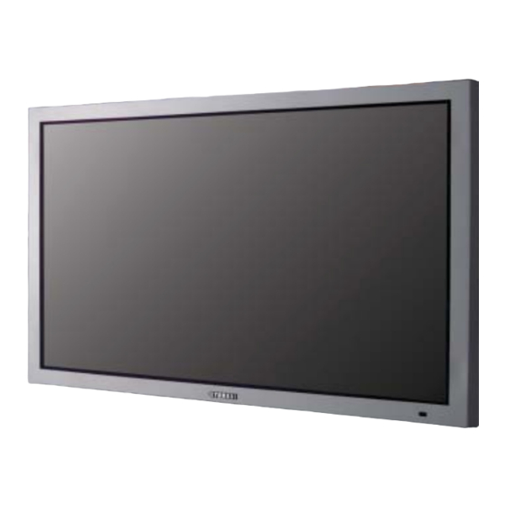
Page 1: Plasma Display
Hyundai Plasma Display PD421 Svc Manual... - Page 2 Plasma Display PD421 . Circuit Service Methods 1. W hite Ba lance A djustment l Refer to adjustment specifications for information on makin g adjustments m When white balance has to be adjusted during service - If the module is replaced, it must be readjusted u sing VG -828 equipment,...
- Page 3 After selecting AD9883 After ROM or B/D enter(c) Data recorded replaced in R,G and B-Gain and Bi as values separately Select the Video mode After exiting from the Factory select the PC mode Enter in to the Factory mode Enter the Facrory to select the PC mode After selecting "Whte"...
-
Page 4: Dvi Mode
SIL161B is an output port and is activated when pin nu mber 2 is high. DTV signa ls 480p, 720p, and 1080i can be displayed through the DVI port . However, PD421 cannot only display 60Hz DTV signals. It is unable to display 50Hz DTV signals. PC can support both 50Hz and 60Hz signals. - Page 5 2) DTV Mode DTV signals are entered as Y, P b(Cb), and Pr(Cr) component signals, separated into Y, Cb, Cr, H, and V sync on (xan51AcuxA01) and entered to BA7 657. If pin 1 6 is low, DTV signals are entered into ADC9883. In the AD9883, like the PC signals, the DTV signals are converted to 24 bits and entered into scalar ASI500.
- Page 6 Plasma Display PD421 color signals. The NT SC and PAL /SECAM are automatically detected by the video decoders, main VPC3230 and sub VPC3230, and converted to Y (8bits) and UV (8bits) and sent to the deinterla cer IC, FLI2310, as 16bit digital signal.
- Page 7 Plasma Display PD421 7) PIP/POP Support Mode Map S-VHS Video Scart Main S-VHS Video Scart X: Not supported, O: Supported Note: When displaying NT SC or P AL signals to PIP or POP , if the signals are displayed as Main: NT SC, Sub: P AL or in reverse, the picture can be seen, but the size scaling for the sub-scr een will not display properly.
- Page 8 Plasma Display PD421 Audio input signal for PC/DVI, DT V, and DV D modes is entered into the audio processor IC, MSP3450G , and audio input signal for VID E O/S -VIDEO, and SCART modes is first selected in MUX 8851 a nd entered into the audio processor.
- Page 9 B ar This occ urs when the FPC wire, which connects the address line below the module, is damaged. Because the wi re is on the bottom, it can be e asily damaged when the module is lifted and assembled or from external shock. Use caution when handling the module and use the handle on the bottom of the module to lift or move.
-
Page 10: Critical Parts Specification
Plasma Display PD421 Critical Parts Specification AD9883 MC68HC705BD7B Sync Detect fo ugg ng Midscale Clamping CLAMP A IN OUTA Power-Down Mode Low Power : 500mW tYPICAL MIDSCV Composite Sync Applications Require an External Coast HSYNC DTACK SYNC COAST PROCESSING HSOUT... - Page 11 AD9883–SPECIFICA TIONS Analog Interface = 3.3 V, V = 3.3 V, ADC Clock = Maximum Conversion Rate) T est AD9883KST-110 Parameter Temp Level Unit RESOLUTION Bits DC ACCURACY Differential Nonlinearity 25 C +1.25/–1.0 Full +1.35/–1.0 Integral Nonlinearity 25 C 1.85 Full No Missing Codes Full...
- Page 12 Plasma Display PD421 Test AD9883KST-110 Parameter Temp Level Unit POWER SUPPLY Supply Voltage Full Supply Voltage Full Supply Voltage Full Supply Current (V ) Supply Current (V 25 C Supply Current (P ) Total Power Dissipation Full Power-Down Supply Current...
- Page 13 CXA2151Q MC68HC705BD7B Description 48 pin QFP (Plastic) The CXA2151Q is a bipolar IC developed for multi scan TVs, and incorporates a four system video switch (including HV sync signal processing) and a YCbCr output matrix circuit. Features •Supports the I C bus •Supports multi scan •Four system video switch (of which two systems support D3 pins)
- Page 14 Plasma Display PD421 Block Diagram --13--...
- Page 15 DS90C385 This chipset is an ideal means to solve EMI and cable size General Description problems associated with wide, high-speed TTL interfaces. The DS90C385 transmitter converts 28 bits of LVCMOS/ LVTTL data into four LVDS (Low Voltage Differential Signal- Features ing) data streams.
-
Page 16: Absolute Maximum Ratings
Plasma Display PD421 Absolute Maximum Ratings (Note 1) DS90C385SLC 2.0 W Package Derating: If Military/Aerospace specified devices are required, DS90C385MTD 12.5mW/ C above +25 C please contact the National Semiconductor Sales Office/ Package Derating: Distributors for availability and specifications. DS90C365MTD... - Page 17 Electrical Characteristics (Continued) Over recommended operating supply and temperature ranges unless otherwise specified. Symbol Parameter Conditions Units TRANSMITTER SUPPLY CURRENT ICCTG Transmitter Supply Current = 100 W, f = 32.5MHz 16 Grayscale = 5 pF, f = 40 MHz DS90C365 16 Grayscale Pattern f = 65 MHz (Figures 3, 4)
- Page 18 Plasma Display PD421 Transmitter Switching Characteristics (Continued) Over recommended operating supply and temperature ranges unless otherwise specified Symbol Parameter Max Units TPPos0 Transmitter OutputPulse Positionfor Bit 0 (Figures 13, 14) f = 85 MHz -0.20 0.20 (Note 5) TPPos1 TransmitterOutput Pulse Position for Bit 1 1.48...
- Page 19 P89C51RD2BA DESCRIPTION FEATURES The P89C51RB2/RC2/RD2 device contains a non-volatile 80C51 Central Processing Unit 16kB/32kB/64kB Flash program memory that is both parallel On-chip Flash Program Memory with In-System Programming programmable and serial In-System and In-Application (ISP) and In-Application Programming (IAP) capability Programmable.
- Page 20 Plasma Display PD421 ORDERING INFORMATION PHILIPS MEMOR Y FREQUENCY (MHz) (EXCEPT NORTH PHILIPS NORTH TEMPERA TURE AMERICA AMER CA AMERICA) AMER CA) VOLTAGE VOLTAGE RANGE (5 C) DWG # FLASH 6 CLOCK 12 CLOCK PART ORDER PART ORDER RANGE AND PACKAGE...
-
Page 21: Block Diagram
BLOCK DIAGRAM P0.0±P0.7 P2.0±P2.7 POR T 0 POR T 2 DRIVERS DRIVERS RAM ADDR POR T 0 POR T 2 FLASH REGISTER LATCH LATCH STACK REGISTER POINTER PROGRAM ADDRESS TMP1 REGISTER TMP2 BUFFER SFRs TIMERS INCRE- P.C.A. MENTER PROGRAM COUNTER PSEN DPTR'S TIMING... - Page 22 Plasma Display PD421 S2310 DESCRIPTION The s2300 is a highly integrated digital video standard 2D video decoders, eliminating the format converter for DTV and DVD applications need for expensive 3D video decoders. using patented deinterlacing post DEINTERLACING – processing algorithms...
- Page 23 Port 2 16/20/24-bit 8-bit Noise Reducer, Output RBG/YCrCb Input Processor Vertical and 656 Input Deinterlacer, Frame Processor with Digital Outputs with Auto Sync Horizontal Rate Converter and Sync Generation and auto Adjust Scalers SDRAM interface and DACs RBG/YCrCb Port 1 Analog Outputs 8/16/24-bit RGB/YCrCb...
- Page 24 Plasma Display PD421 Sil161B MC68HC705BD7B General Description Features The SiI 161B receiver uses PanelLink Digital technology to support high • Low Power Operation: 280mA max. current consumption at 3.3V core operation resolution displays up to UXGA. The SiI 161B receiver supports up to true •...
- Page 25 Silicon Image, Inc. Differences Between SiI161A and SiI161B While the SiI161B is pin to pin compatible with the SiI161A, there are minor differences in functions and suggested external component value. When designing the SiI161B into an existing design, note that the recommended external resistor (EXT_RES) value has changed from 560 to 390 to match the impedance of a 50 cable.
- Page 26 Plasma Display PD421 TA2024 MC68HC705BD7B G E N E R A L D E S C R I P T I O N T h e T A 2 0 2 4 i s a 1 5 W / c h c o n t i n u o u s a v e r a g e t w o - c h a n n e l C l a s s - T D i g i t a l A u d i o P o w e r A m p l i f i e r I C u s i n g T r i p a t h ’...
- Page 27 A B S O L U T E M A X I M U M R A T I N G S (Note 1) S YMB OL ARAME TE R Value UNITS S upply Voltage Input S ection Supply Voltage S LE E P S LE E P Input Voltage -0.3 to 6.0...
- Page 28 Plasma Display PD421 P I N D E S C R I P T I O N Function Description 2, 3 DCAP2, DCAP1 Charge pump sw itching pins. DCAP1 (pin 3) is a free running 300kHz square wave between VDDA and DGND (12Vpp nominal). DCAP2 (pin 2) is level shifted 10 volts above DCAP1 (pin 3) w ith the same amplitude (12Vpp nominal), frequency , and phase as DCAP1.
- Page 29 A P P L I C A T I O N / T E S T C I R C U I T TA202 4 VDD1 20KY 10uH, 2A OUTP1 2.2uF 20KY (Pin 35) Processing PGND1 0.47uF & 0.47uF (Pin 35) VDD1 Modulation 0.1uF...
- Page 30 Plasma Display PD421 TA8851 MC68HC705BD7B --29--...
- Page 31 --30--...
- Page 32 Plasma Display PD421 VPC3230 1. Introduction The VPC 323xD is a high-quality, single-chip video - peaking, contrast, brightness, color saturation and front-end, which is targeted for 4:3 and 16:9, 50/60-Hz tint for RGB/ YC and CVBS/S-VHS and 100/120 Hz TV sets. It can be combined with other...
- Page 33 1.2. V id e o P ro cesso r F a m ily T he V P C video pro ces s or fa m ily s upport s 15 /32-k H z s yste m s and i s av ai la ble wi th di ffe rent c om b filter opt ions .
- Page 34 Plasma Display PD421 1.3. VP C Applic ations external sources, such as MP E G -2 set-top boxes in transparent (4:2:2) quality. F urthermore, it transforms F ig. 1ñ2 depicts several VP C applications. S ince the RG B /F ast B lank signals to the common digital video...
- Page 35 uPD64083 MC68HC705BD7B PD 64083 realizes a high precision Y /C separation and a noise reduction by the three-dimension signal processing for N TSC signal. This product has the O n-chip 4Mbit memory for flame delay, 2ch of high precision internal 10bit A/D converter, and adapting 10bit signal processing (only for luminance signal) and high picture quality.
- Page 36 Plasma Display PD421 PIN CONFIGURAT ION (TOP VIEW ) 100-pin plastic Q F P (14 20) PD 64083G F-3BA DG ND DG ND TE S T IC 1 KI L TE S T IC 2 LI N E T E ST 01...
- Page 37 AC I : Analog C (C hroma) Signal Input AC O : Analog C (C hroma) Signal Output AG ND : Analog Section G round ALT F : Alternate Flag for D igital Y/C Output AVD D : Analog Section Power Supply AY I : Analog Y (Luma) Signal Input AY O...
- Page 38 Plasma Display PD421 BLOCK DIA GRAM E X TDY C O 9-0 D Y C O E rror S e lect VC LY D YC O 9-0 detection EXT ALTF ALTF C lamp Y C N R Y -high freq.
- Page 39 Hyundai ImageQuest PT421H 01. Cover Page 02. Block Diagram Working Board Schematic(GRAPHIC) 03. VGA Analog Input 04. CXA2151Q 05. ADC-AD9883(140M) (ASI500) 06. TMDS RECEIVER SIL161B-140 07. Damping Network 08. ASI500 09. ASI500 DECOUPLE CAPS 10. FRAME BUFFER MEMORY 11. LVDS TRANSMITTER(DS90C385MTD) 12.
- Page 40 CVBS PART R/L_In PC/DVI Sound R/L_In Processor MSP3450G RS-232 NORMAL R/L_In Expansion TEA2025D Speaker KEY PAD R/L_In WOFER Full_Scart R/L_Out Half_Scart Tuner_Main Tuner_Sub Hyundai ImageQuest R/L_Out Title PT421H BLOCK DIAGRAM Size Document Number E42095419 Date: Thursday, September 18, 2003 Sheet...
- Page 41 AUDTV1A RI15 AUDIO L_R CI03 DI12 COMP1C COMP2C BAV99 LI10 LC2012-121 LI15 LC2012-121 DTV_Pr DVD_Cr graphic pg4 graphic pg4 COMPONENT_Y_Pb_Pr COMPONENT_Y_Pb_Pr RI32 CI26 RI25 CI33 Hyundai Image Quest Title VGA Analog Input Size Document Number Custom E42095419 Date: Sheet...
- Page 42 CXA09 10pF YG_OUT EXTCLK CXA08 YG_IN RXA05 IREF *1) 4MHz Crystal QXA01 10K Metal Film Resistor Oscillator KSA1182-Y *2) One of Q1 or R should be removed. RXA04 Hyundai Image Quest Title VCC_5A CXA2151Q Size Document Number E42095419 Date: Sheet...
- Page 43 CA57 RA30 2K QA02 DTV_VOUT graphic pg4 KSC1623-Y RA21 2K 74HCT86 CA54 74HCT86 DA02 RA31 CA58 100K 22uF 16V 1N4148 SOT-23 22uF 16V PCDTV_SEL graphic pg13 CA59 PC(1),DTV(0) Hyundai Image Quest Title ADC-ADC9883 Size Document Number Custom E42095419 Date: Sheet...
- Page 44 BAV99 DDC_SCL2 High - dual pixels/ Clk High - high out drive strength DDC_SDA2 STAG_OUT Low - ODCK runs continuously Hyundai Image Quest ZDT1 24LC21 SMD EEPROM ZDT2 High - ODCK stop when DE low RLZ 5.6V Title TMDS Receiver SIL161B RLZ 5.6V...
- Page 45 IBODD[0..7] graphic pg6 DBODD[0..7] RDAR23 33 ARRAY DBODD0 IBODD0 DBODD1 IBODD1 DBODD2 IBODD2 DBODD3 IBODD3 RDAR24 33 ARRAY DBODD4 IBODD4 DBODD5 IBODD5 DBODD6 IBODD6 DBODD7 IBODD7 Hyundai Image Quest Title Damping Network Size Document Number E42095419 Date: Sheet...
- Page 46 AFT1_ADC video pg8 SCL_3 GPIO0 GPIO1 GPIO2 GPIO3 GPIO4 video pg8 NT_PAL_SEL FLI_DE video pg4,6 SVIDEO_DE RSC51 RSC53 RSC55 RSC57 RSC17 FLI_H FLI_CLK FLI_V CONN RCPT 11x2 Hyundai Image Quest Title ASI500 Size Document Number Custom E42095419 Date: Sheet...
- Page 47 GOUT17 CSC78 CSC79 CSC80 CSC81 CSC82 CSC83 CSC84 CSC85 CSC86 BOUT1[0..7] graphic pg8 RSAR11 NC BOUT10 BOUT11 BOUT12 BOUT13 RSAR12 NC BOUT14 BOUT15 BOUT16 BOUT17 OPTION Hyundai Image Quest Title ASI500 Decouple Caps Size Document Number Custom E42095419 Date: Sheet...
- Page 48 K4S643232C graphic pg8 AMA[0..10] ADQM[0..7] graphic pg8 ACKE graphic pg8 RFB10 ASI500 : RFB10 : NC , RFB11: 0 OHM Hyundai Image Quest K4S643232C Title RFB11 ASI510 : RFB10 : 4.7K , RFB11: NC Frame Buffer Memory (MT48LC4M32B2TG D3.3V Size...
- Page 49 RLV01 /PWR_DWN 4.7K graphic pg13 LVDS_EN RXE0- ACTIVE_LOW DS90C385MTD RXE0+ RXE1- RXE1+ RXE2- RXE2+ RXEC- RXEC+ RXE3- RXE3+ RLV03 graphic pg13 SCL_3 graphic pg13 SDA_3 RLV04 CON31 Hyundai Image Quest Title LVDS Transmitter DS90C385MTD Size Document Number E42095419 Date: Sheet...
- Page 50 CAU19 3.3uF 50V CAU26 SCL_5 graphic pg3 RAU59 SDA_5 4.7K graphic pg3 RESET_Mn RESET_Mn MUTE graphic pg13 ACTIVE_LOW RAU60 QAU01 graphic pg12 AUDIO_MUTE KSC1623-Y RAU91 CAU05 Hyundai Image Quest Title MSP3450 Audio Processor Size Document Number Custom E42095419 Date: Sheet...
- Page 51 /1SD S3.3V 74LVC373AD-SOT163-1 EXPAN_OUT1 FBM07 CMC26 CMC48 CMC50 /2SD 600 ohm 0.5A 2012 RMC49 74LVC373AD-SOT163-1 4.7K CMC37 NT_PAL_SEL graphic pg13 QMC06 KSC1623-Y Hyundai ImageQuest RMC101 Title 4.7K MICROCONTROLLER SDA5550 Size Document Number Custom E42095419 Date: Thursday, September 18, 2003 Sheet...
- Page 52 UP03 LPM01 COIL 47UH LPM09 BEAD 4532 A3.3V CP10 CP02 CP01 CP33 CP09 100uF 16V BA033FP 100uF 16V UP02 LPM03 COIL 47UH A12V CP38 CP39 CP23 CP37 CNPR1 100uF 16V BA05FP 100uF 16V CP25 A12V 12Vamp 12Vamp VT33V GND-amp LPM10 COIL 47UH GND-amp UP01...
- Page 53 R2IN MAX232C CRS06 10uF 16V 15V 0.5W SOT-23 CNI1 24V 0.5W SOT-23 15V 0.5W SOT-23 24V 0.5W SOT-23 DB9 Female Rt Angle w/Mount Latch SERIAL PORT Hyundai ImageQuest Title MAX232C Size Document Number E42095419 Date: Thursday, September 18, 2003 Sheet...
- Page 54 1N4148 SOT-23 CNK1 LEFT RIGHT LEDG LEDR Lumex Opto, Inc. SSL-LX3059IGW 2mm 14PIN DIP SWK06 SWK01 SWK02 SWK03 SWK04 SWK05 SWK07 LEFT POWER SOURCE DOWN MENU RIGHT Hyundai Image Quest Title Remocon & Keypad Size Document Number E42095417 Date: Sheet...
- Page 55 Hyundai ImageQuest 01. Cover Page 02. MUX 03. 3D COMBFILTER PT421H 04. VPC3230(MAIN) 05. VPC3230(SUB) 06. FIFO MEMORY Schematic Diagram(VIDEO) 07. FLI2300 08. INPUT BOARD Date:05/29/2003 Hyundai Image Quest Title PD421 SCHEMATIC DIAGRAM Size Document Number E42095417 Date: Sheet...
- Page 56 1) CXA2069 :A5V - 72mA 2) TUNER :A33 - Tuning Voltage TUNER_CVBS1 RMX26 CMX23 1uF 50V VOUT1 RMX06 CMX26 1uF 50V A5V - 80mA(40mA*2) HS_CVBS(Y) video pg8 YIN1 3D_Y RMX18 CMX12 1uF 50V CMX31 1uF 16V UMX02 FS_CVBS(Y) D3.3V LUMA_IN YOUT1 TUNER_CVBS2 CMX30...
- Page 57 CCF51 3D_D3.3V 10uF 16V CCF42 CCF49 CCF46 CCF45 47uF 16V BA033FP 47uF 16V 3D_A2.5V CCF35 CCF44 CCF43 UCF02 CCF47 47uF 16V RC1117ST-2.5V 47uF 16V Hyundai Image Quest Title 3Dcomp Size Document Number Custom E42095417 Date: Saturday, August 23, 2003 Sheet...
- Page 58 CDM74 10uF 16V CDM72 103 video pg7 TTX_R CDM64 10uF 16V CDM70 103 SC1_G video pg7 CDM63 103 CDM67 10uF 16V Hyundai Image Quest video pg7 TTX_G CDM75 10uF 16V Title SC1_R video pg7 CDM68 103 CDM71 103 VPC3230 Video Decoder(Main)
- Page 59 CDS41 CDS43 CDS44 CDS36 D3.3V RDS34 RDS32 RDS31 RDS33 SC1_FB 3230_DVD_Cb SC1_B video pg8 3230_DVD_Y SC1_G 3230_DVD_Cr SC1_R (DVD 480I) video pg8 Hyundai Image Quest Title VPC3230 Video Decoder(SUB) Size Document Number Custom E42095417 Date: Saturday, August 23, 2003 Sheet...
- Page 60 : RFM10 : OPEN , RFM02 : 0 SVPC_Y5 SVPC_Y6 SVPC_Y7 video pg5 MS_RSTW video pg5 MS_IE video pg5 MS_WE MS_RSTR video pg4 MS_RE video pg4 MS_OE video pg4 Hyundai Image Quest Title FIFO Memory Size Document Number E42095417 Date: Sheet...
- Page 61 CFL47 CFL52 10uF 16V UFL2 KS643232C D1.8V LFL06 DAC1.8V BEAD 4532 CFL48 CFL49 10uF 16V LFL07 PLL1.8V BEAD 4532 CFL50 CFL51 10uF 16V Hyundai Imagequest FLI_SDD[31:0] Pg15 Title FLI2300 Size Document Number Custom E42095417 Date: Saturday, August 23, 2003 Sheet...
- Page 62 CVO12 LVO13 LC2012-121 RVO26 MONITOR_OUT CVBS1B RVO09 HALF SCART LVO01 LC2012-121 RVO13 AUDIO_R_OUT RVO27 CVBS_VIDEO&AUDIO LVO23 LC2012-121 HS_CVBS(Y) video pg2 HS_CVBS(Y) CVBS1C RVO72 Hyundai Image Quest LVO06 LC2012-121 Title AUDIO_L_OUT INPUT BOARD RVO24 CVBS_VIDEO&AUDIO Size Document Number E42095417 Date: Sheet...
- Page 63 PART LIST LOCATION PART NUMBER DESCRIPTION REMARK 2011000006 CAP-AL-C,10UF 16V M 4052 2011000006 CAP-AL-C,10UF 16V M 4052 2011000006 CAP-AL-C,10UF 16V M 4052 CAU10 2011000006 CAP-AL-C,10UF 16V M 4052 CAU13 2011000006 CAP-AL-C,10UF 16V M 4052 CAU14 2011000006 CAP-AL-C,10UF 16V M 4052 CAU17 2011000006 CAP-AL-C,10UF 16V M 4052...
- Page 64 LOCATION PART NUMBER DESCRIPTION REMARK CSC89 2011000006 CAP-AL-C,10UF 16V M 4052 CSC91 2011000006 CAP-AL-C,10UF 16V M 4052 CSC93 2011000006 CAP-AL-C,10UF 16V M 4052 CT03 2011000006 CAP-AL-C,10UF 16V M 4052 CT17 2011000006 CAP-AL-C,10UF 16V M 4052 CXA13 2011000006 CAP-AL-C,10UF 16V M 4052 CXA14 2011000006 CAP-AL-C,10UF 16V M 4052...
- Page 65 LOCATION PART NUMBER DESCRIPTION REMARK CMX31 2011010014 CAP-AL-C,100UF 16V M 6357 CAU38 2011010014 CAP-AL-C,100UF 16V M 6357 CP01 2011010014 CAP-AL-C,100UF 16V M 6357 CP05 2011010014 CAP-AL-C,100UF 16V M 6357 CP08 2011010014 CAP-AL-C,100UF 16V M 6357 CP09 2011010014 CAP-AL-C,100UF 16V M 6357 CP12 2011010014 CAP-AL-C,100UF 16V M 6357...
- Page 66 LOCATION PART NUMBER DESCRIPTION REMARK CAU51 2013390003 CAP-AL-C,3.3UF 50V M 4052 CAU64 2014700009 CAP-AL-C,47UF 16V M 6352 CDM30 2014700009 CAP-AL-C,47UF 16V M 6352 CDS29 2014700009 CAP-AL-C,47UF 16V M 6352 CSC87 2014700009 CAP-AL-C,47UF 16V M 6352 CXA15 2014700009 CAP-AL-C,47UF 16V M 6352 CCF01 2014700009 CAP-AL-C,47UF 16V M 6352...
- Page 67 LOCATION PART NUMBER DESCRIPTION REMARK CT21 2121010035 CAP-C-C,100PF 50V J COG 1608 CMX09 2121010035 CAP-C-C,100PF 50V J COG 1608 CMX10 2121010035 CAP-C-C,100PF 50V J COG 1608 CVO25 2121020039 CAP-C-C,1000PF 50V K X7R 1608 CVO26 2121020039 CAP-C-C,1000PF 50V K X7R 1608 CVO27 2121020039 CAP-C-C,1000PF 50V K X7R 1608...
- Page 68 LOCATION PART NUMBER DESCRIPTION REMARK CFB16 2121030061 CAP-C-C,0.01UF 50V K X7R 1608 CFB18 2121030061 CAP-C-C,0.01UF 50V K X7R 1608 CFB20 2121030061 CAP-C-C,0.01UF 50V K X7R 1608 CFB25 2121030061 CAP-C-C,0.01UF 50V K X7R 1608 CFB27 2121030061 CAP-C-C,0.01UF 50V K X7R 1608 CXA18 2121030061 CAP-C-C,0.01UF 50V K X7R 1608...
- Page 69 LOCATION PART NUMBER DESCRIPTION REMARK CM23 2121040045 CAP-C-C,0.1UF 50V Z Y5V 1608 CM24 2121040045 CAP-C-C,0.1UF 50V Z Y5V 1608 CM39 2121040045 CAP-C-C,0.1UF 50V Z Y5V 1608 CM40 2121040045 CAP-C-C,0.1UF 50V Z Y5V 1608 CP02 2121040045 CAP-C-C,0.1UF 50V Z Y5V 1608 CP04 2121040045 CAP-C-C,0.1UF 50V Z Y5V 1608...
- Page 70 LOCATION PART NUMBER DESCRIPTION REMARK CAU52 2121040045 CAP-C-C,0.1UF 50V Z Y5V 1608 CAU63 2121040045 CAP-C-C,0.1UF 50V Z Y5V 1608 CAU68 2121040045 CAP-C-C,0.1UF 50V Z Y5V 1608 CAU75 2121040045 CAP-C-C,0.1UF 50V Z Y5V 1608 CA08 2121040045 CAP-C-C,0.1UF 50V Z Y5V 1608 CA09 2121040045 CAP-C-C,0.1UF 50V Z Y5V 1608...
- Page 71 LOCATION PART NUMBER DESCRIPTION REMARK CFB28 2121040045 CAP-C-C,0.1UF 50V Z Y5V 1608 CI04 2121040045 CAP-C-C,0.1UF 50V Z Y5V 1608 CI05 2121040045 CAP-C-C,0.1UF 50V Z Y5V 1608 CI19 2121040045 CAP-C-C,0.1UF 50V Z Y5V 1608 CLV10 2121040045 CAP-C-C,0.1UF 50V Z Y5V 1608 CLV11 2121040045 CAP-C-C,0.1UF 50V Z Y5V 1608...
- Page 72 LOCATION PART NUMBER DESCRIPTION REMARK CXA11 2121040045 CAP-C-C,0.1UF 50V Z Y5V 1608 CXA12 2121040045 CAP-C-C,0.1UF 50V Z Y5V 1608 CCF03 2121040045 CAP-C-C,0.1UF 50V Z Y5V 1608 CCF05 2121040045 CAP-C-C,0.1UF 50V Z Y5V 1608 CCF06 2121040045 CAP-C-C,0.1UF 50V Z Y5V 1608 CCF07 2121040045 CAP-C-C,0.1UF 50V Z Y5V 1608...
- Page 73 LOCATION PART NUMBER DESCRIPTION REMARK CFL09 2121040045 CAP-C-C,0.1UF 50V Z Y5V 1608 CFL10 2121040045 CAP-C-C,0.1UF 50V Z Y5V 1608 CFL11 2121040045 CAP-C-C,0.1UF 50V Z Y5V 1608 CFL12 2121040045 CAP-C-C,0.1UF 50V Z Y5V 1608 CFL13 2121040045 CAP-C-C,0.1UF 50V Z Y5V 1608 CFL14 2121040045 CAP-C-C,0.1UF 50V Z Y5V 1608...
- Page 74 LOCATION PART NUMBER DESCRIPTION REMARK CFL47 2121040045 CAP-C-C,0.1UF 50V Z Y5V 1608 CFL48 2121040045 CAP-C-C,0.1UF 50V Z Y5V 1608 CFL50 2121040045 CAP-C-C,0.1UF 50V Z Y5V 1608 CFM01 2121040045 CAP-C-C,0.1UF 50V Z Y5V 1608 CFM02 2121040045 CAP-C-C,0.1UF 50V Z Y5V 1608 CFM03 2121040045 CAP-C-C,0.1UF 50V Z Y5V 1608...
- Page 75 LOCATION PART NUMBER DESCRIPTION REMARK CDS15 2121520011 CAP-C-C,1500PF 50V J X7R 1608 CDS23 2121520011 CAP-C-C,1500PF 50V J X7R 1608 CDS28 2121810013 CAP-C-C,180PF 50V J COG 1608 CDS31 2121810013 CAP-C-C,180PF 50V J COG 1608 CDS45 2121810013 CAP-C-C,180PF 50V J COG 1608 CT05 2122210028 CAP-C-C,220PF 50V J COG 1608...
- Page 76 LOCATION PART NUMBER DESCRIPTION REMARK CDM34 2122240044 CAP-C-C,0.22UF 50V Z Y5V 1608 CDM35 2122240044 CAP-C-C,0.22UF 50V Z Y5V 1608 CDM36 2122240044 CAP-C-C,0.22UF 50V Z Y5V 1608 CDM38 2122240044 CAP-C-C,0.22UF 50V Z Y5V 1608 CDM39 2122240044 CAP-C-C,0.22UF 50V Z Y5V 1608 CDM40 2122240044 CAP-C-C,0.22UF 50V Z Y5V 1608...
- Page 77 LOCATION PART NUMBER DESCRIPTION REMARK CDS19 2123910017 CAP-C-C,390PF 50V J COG 1608 CDS20 2123910017 CAP-C-C,390PF 50V J COG 1608 CDM09 2123910017 CAP-C-C,390PF 50V J COG 1608 CDM17 2123910017 CAP-C-C,390PF 50V J COG 1608 CDS09 2123910017 CAP-C-C,390PF 50V J COG 1608 CDS16 2123920015 CAP-C-C,3900PF 50V K X7R 1608...
- Page 78 LOCATION PART NUMBER DESCRIPTION REMARK CXA22 2125600009 CAP-C-C,56PF 50V J COG 1608 CDM12 2126830010 CAP-C-C,0.068UF 16V K X7R 1608 CAU36 2126830010 CAP-C-C,0.068UF 16V K X7R 1608 CAU37 2126840013 CAP-C-C,0.68UF 50V Z Y5V 1608 CDM27 2126840013 CAP-C-C,0.68UF 50V Z Y5V 1608 CDS27 2126840013 CAP-C-C,0.68UF 50V Z Y5V 1608...
- Page 79 LOCATION PART NUMBER DESCRIPTION REMARK RDAR20 2593309004 RES-C-NET,33 0.063W J 3216 RDAR21 2593309004 RES-C-NET,33 0.063W J 3216 RDAR22 2593309004 RES-C-NET,33 0.063W J 3216 RDAR23 2593309004 RES-C-NET,33 0.063W J 3216 RDAR24 2593309004 RES-C-NET,33 0.063W J 3216 RSAR01 2593309004 RES-C-NET,33 0.063W J 3216 RSAR02 2593309004 RES-C-NET,33 0.063W J 3216...
- Page 80 LOCATION PART NUMBER DESCRIPTION REMARK RDM53 2604703009 RES-C,470K 0.1W J 1608 RVO60 2604703009 RES-C,470K 0.1W J 1608 RVO62 2604709017 RES-C,47 0.1W J 1608 RA01 2605100008 RES-C,510 0.063W J 1608 RFL20 2605100008 RES-C,510 0.063W J 1608 RDS10 2605100008 RES-C,510 0.063W J 1608 RMX01 2605600015 RES-C,560 0.1W J 1608...
- Page 81 LOCATION PART NUMBER DESCRIPTION REMARK RXA09 2607509011 RES-C,75 0.1W J 1608 RXA10 2607509011 RES-C,75 0.1W J 1608 RXA11 2607509011 RES-C,75 0.1W J 1608 RXA12 2607509011 RES-C,75 0.1W J 1608 RXA13 2607509011 RES-C,75 0.1W J 1608 RDM30 2607509011 RES-C,75 0.1W J 1608 RDM31 2607509011 RES-C,75 0.1W J 1608...
- Page 82 LOCATION PART NUMBER DESCRIPTION REMARK RVO72 3011200001 PDP,S42SD-YDXX PD421 RAU56 3100500198 DI-SW,BAV99 SMD 3100500198 DI-SW,BAV99 SMD 3100500198 DI-SW,BAV99 SMD DI01 3100500198 DI-SW,BAV99 SMD DI02 3100500198 DI-SW,BAV99 SMD DI03 3100500198 DI-SW,BAV99 SMD DI08 3100500198 DI-SW,BAV99 SMD DI09 3100500198 DI-SW,BAV99 SMD DI10...
- Page 83 LOCATION PART NUMBER DESCRIPTION REMARK 3101000394 DI-ZN,RLZTE-1115B 3101000394 DI-ZN,RLZTE-1115B 3101000394 DI-ZN,RLZTE-1115B 3104100145 DI-SCHOT,MBRS130T3 SMD 3104100145 DI-SCHOT,MBRS130T3 SMD 3104100145 DI-SCHOT,MBRS130T3 SMD DAU1 3104100145 DI-SCHOT,MBRS130T3 SMD DAU2 3110100762 TR-GEN,KSC1623 SMD DAU3 3110100762 TR-GEN,KSC1623 SMD DAU4 3110100762 TR-GEN,KSC1623 SMD QAU01 3110100762 TR-GEN,KSC1623 SMD QA01 3110100762 TR-GEN,KSC1623 SMD...
- Page 84 LOCATION PART NUMBER DESCRIPTION REMARK UP04 3200001571 IC-LIN,BA17808FP-E2 UDM02 3200001572 IC-LIN,BA17809FP-E2 UA02 3200001573 IC-LIN,BA033FP-E2 UP06 3200001573 IC-LIN,BA033FP-E2 UP01 3200001574 IC-LIN,TA8851BN DIP UP03 3200001575 IC-LIN,ST232CDR UCF03 3200001576 IC-LIN,SIL161B QFP UMX01 3200001577 IC-LIN,CXA2151Q QFP URS01 3200001578 IC-LIN,PD64083 QFP UT02 3200001579 IC-LIN,LM1117MP-1.8 SOT223 UXA01 3200001580 IC-LIN,BA7657F-E2...
- Page 85 LOCATION PART NUMBER DESCRIPTION REMARK UFL1 3205001413 IC-U,ASI500 BGA IMAGE PRO UDM01 3205001414 IC-U,MSP3450G PMQFP SOUND UDS01 3205001415 IC-U,P89C51RD2BA PLCC MCU USC01 3330600488 LED,SML-010LTT86N UAU2 3330600488 LED,SML-010LTT86N UM01 3500101878 CHIP-INDUCTOR,LMFC3225T3R DT01 3500101878 CHIP-INDUCTOR,LMFC3225T3R DT16 3500101878 CHIP-INDUCTOR,LMFC3225T3R LDM03 3500101878 CHIP-INDUCTOR,LMFC3225T3R LDM04 3500101878 CHIP-INDUCTOR,LMFC3225T3R LDM05...
- Page 86 LOCATION PART NUMBER DESCRIPTION REMARK LMX01 3500101885 CHOKE-COIL,56uH 8x11 LAU2 3500101885 CHOKE-COIL,56uH 8x11 LAU3 3520200199 FLT-LC,H354LAI-K5202=P3 LAU4 3520200199 FLT-LC,H354LAI-K5202=P3 LAU7 3520200200 FLT-LC,H354BAI-K5110=P3 FCF01 3530200621 VIB-QUARTZ,DIP 4MHZ 100PF FDM02 3530200622 VIB-QUARTZ,DIP 20MHZ 22PF FDM01 3530200622 VIB-QUARTZ,DIP 20MHZ 22PF XXA01 3530200623 VIB-QUARTZ,DIP 18.432MHZ XM01 3530200624 VIB-QUARTZ,DIP 20.25MHZ...
- Page 87 LOCATION PART NUMBER DESCRIPTION REMARK LVO02 3540800060 COR-CHP,FI-B2012-222KJT LVO03 3540800060 COR-CHP,FI-B2012-222KJT LVO04 3540800060 COR-CHP,FI-B2012-222KJT LVO05 3540800060 COR-CHP,FI-B2012-222KJT LVO06 3540800060 COR-CHP,FI-B2012-222KJT LVO07 3540800064 COR-CHP,HH-1M4532-121JT LVO08 3540800064 COR-CHP,HH-1M4532-121JT LVO10 3540800064 COR-CHP,HH-1M4532-121JT FA01 3540800064 COR-CHP,HH-1M4532-121JT FA02 3540800064 COR-CHP,HH-1M4532-121JT FA03 3540800064 COR-CHP,HH-1M4532-121JT FT01 3540800064 COR-CHP,HH-1M4532-121JT FT02 3540800064...
- Page 88 LOCATION PART NUMBER DESCRIPTION REMARK LFL05 3540800064 COR-CHP,HH-1M4532-121JT LFL06 3610200115 BATTERY,AA 1.5V MERCURY&CADMIU LFL07 3720101388 CONN-M,SMW200-06P LFL08 3720101388 CONN-M,SMW200-06P 3720101396 CONN-M,SMW250-02 2 CNAU3 3720101397 CONN-M,SMW250-03 3 CNMX1 3720101401 CONN-M,SMW250-08 8 SPKR1 3720101401 CONN-M,SMW250-08 8 SPKL1 3720101403 CONN-M,SMW250-10 10 CNPR2 3720101404 CONN-M,SMW250-11 11 CNFL2 3720101916...
- Page 89 REMARK 5004000218 SCR-MC BIN+MC3*16 5004000219 SCR-MC BIN+MC8*14(백색아연도금 5004000222 SCR-MC BIN + MC 4*10(백색아연 6101220101 REAR COVER PDP42 6101221201 PD421 REAR COVER ASSY 6110279900 FILTER BRKT V,P421 6110279900 FILTER BRKT V,P421 6110280000 FILTER BRKT H(TOP),P421 6110280001 FILTER BRKT H(BOTTOM),P421 6110280100 SPEAKER BRKT JACK,P421...
- Page 90 PE_BAG(SET) P421 6253119500 CUSHION TOP,P421 6253119600 CUSHION BOTTOM,P421 6253119601 CUSHION MIDDLE,P421 6301191400 PALLET PAD,ALL MODEL,SW-3 6301194000 PD421 CTN BOX TOP IQT ALL 6301194100 42INCH PDP BOX CARTON(BOTTOM) 6309037300 PAD,PALLET ANGLE 201109000401 CAP-AL-C,1UF 50V M 4052 201109000401 CAP-AL-C,1UF 50V M 4052 301070082701...
- Page 91 E4001020808J CAP,CHIP 50V 47PF J 1608 1024 DI06 E42027039010 SWITCH TACT,5MM 160GF VERTICAL 1025 DCF01 E4205020601 MAIN ASS'Y(M1),PD421 1026 CI14 E4208422811 PCBA GRAPHIC TOP(AM),PD421 1027 SWM01 E4208422812 PCBA VIDEO(AM),PD421 1028 E4208422821 PCBA GRAPHIC BOTTOM(AM),PD421 1029 E4208522801 PCBA GRAPHIC(MM),PD421 1030 E4208522802...
- Page 92 LOCATION PART NUMBER DESCRIPTION REMARK 1043 RAU54 RK1JC0T0000J RES-C,0 0.063W J 1608 1044 RAU90 RK1JC0T0000J RES-C,0 0.063W J 1608 1045 RAU91 RK1JC0T0000J RES-C,0 0.063W J 1608 1046 RA04 RK1JC0T0000J RES-C,0 0.063W J 1608 1047 RA05 RK1JC0T0000J RES-C,0 0.063W J 1608 1048 RA06 RK1JC0T0000J...
- Page 93 LOCATION PART NUMBER DESCRIPTION REMARK 1079 RDM63 RK1JC0T0000J RES-C,0 0.063W J 1608 1080 RDM65 RK1JC0T0000J RES-C,0 0.063W J 1608 1081 RDS02 RK1JC0T0000J RES-C,0 0.063W J 1608 1082 RDS04 RK1JC0T0000J RES-C,0 0.063W J 1608 1083 RDS09 RK1JC0T0000J RES-C,0 0.063W J 1608 1084 RDS11 RK1JC0T0000J...
- Page 94 LOCATION PART NUMBER DESCRIPTION REMARK 1115 RM35 RK1JC0T0101J RES-C,100 0.063W J 1608 1116 RM36 RK1JC0T0101J RES-C,100 0.063W J 1608 1117 RM37 RK1JC0T0101J RES-C,100 0.063W J 1608 1118 RM38 RK1JC0T0101J RES-C,100 0.063W J 1608 1119 RM39 RK1JC0T0101J RES-C,100 0.063W J 1608 1120 RM40 RK1JC0T0101J...
- Page 95 LOCATION PART NUMBER DESCRIPTION REMARK 1151 RVO63 RK1JC0T0101J RES-C,100 0.063W J 1608 1152 RVO64 RK1JC0T0102J RES-C,1K 0.063W J 1608 1153 RVO65 RK1JC0T0102J RES-C,1K 0.063W J 1608 1154 RVO69 RK1JC0T0102J RES-C,1K 0.063W J 1608 1155 RAU17 RK1JC0T0102J RES-C,1K 0.063W J 1608 1156 RAU18 RK1JC0T0102J...
- Page 96 LOCATION PART NUMBER DESCRIPTION REMARK 1187 RCF23 RK1JC0T0102J RES-C,1K 0.063W J 1608 1188 RDM06 RK1JC0T0102J RES-C,1K 0.063W J 1608 1189 RDM14 RK1JC0T0102J RES-C,1K 0.063W J 1608 1190 RDM25 RK1JC0T0102J RES-C,1K 0.063W J 1608 1191 RDM54 RK1JC0T0102J RES-C,1K 0.063W J 1608 1192 RDS19 RK1JC0T0102J...
- Page 97 LOCATION PART NUMBER DESCRIPTION REMARK 1223 RAU53 RK1JC0T0151F R-CP 150 1% 1/16 1608 1224 RM02 RK1JC0T0151F R-CP 150 1% 1/16 1608 1225 RSC10 RK1JC0T0151F R-CP 150 1% 1/16 1608 1226 RM30 RK1JC0T0151F R-CP 150 1% 1/16 1608 1227 RSC23 RK1JC0T0152J RES-C,1.5K 0.063W J 1608 1228 RP03...
- Page 98 LOCATION PART NUMBER DESCRIPTION REMARK 1259 RFL25 RK1JC0T0220J RES-C,22 0.063W J 1608 1260 RFL26 RK1JC0T0221J RES-C,220 0.063W J 1608 1261 RFL27 RK1JC0T0221J RES-C,220 0.063W J 1608 1262 RFL28 RK1JC0T0221J RES-C,220 0.063W J 1608 1263 RSC22 RK1JC0T0221J RES-C,220 0.063W J 1608 1264 RCF09 RK1JC0T0222J...
- Page 99 LOCATION PART NUMBER DESCRIPTION REMARK 1295 RDM44 RK1JC0T0471J RES-C,470 0.063W J 1608 1296 RDM45 RK1JC0T0471J RES-C,470 0.063W J 1608 1297 RDM49 RK1JC0T0471J RES-C,470 0.063W J 1608 1298 RDM50 RK1JC0T0471J RES-C,470 0.063W J 1608 1299 RDM51 RK1JC0T0471J RES-C,470 0.063W J 1608 1300 RDS03 RK1JC0T0471J...
- Page 100 LOCATION PART NUMBER DESCRIPTION REMARK 1331 RVO07 TT2N3904D TR,SMD 2N3904D TAPPING 1332 RVO08 TT2N3904D TR,SMD 2N3904D TAPPING 38/ 38...
- Page 101 STAND ASSY PD421 5001000579 SCR-MC BIN MC3X8 3010100140 SHIELD TOP PD421 A5052P T=1.0 5004000219 SCR-MC BIN+MC 8X14 6201326600 REAR COVER CAP PD421 ABS 94-HB 5004000217 SCR-TT BIN MC4*10 6101221200 REAR COVER ASSY PD421 A5052P T=1.0 M11173008012 SCREW FLT(+) M3x8 MSZPC...
Need help?
Do you have a question about the PD421 and is the answer not in the manual?
Questions and answers