
Summary of Contents for HiTech Global HTG-ZRF8
- Page 1 HTG-ZRF8 Platform User Manual HiTech Global ZYNQ UltraScale+™ RFSoC Development Platform HTG-ZRF8 User Manual Version 1.0 August 2018 Copyright © HiTech Global 2004-2018 www.HiTechGlobal.com...
- Page 2 Disclaimer HiTech Global does not assume any liability arising out of the application or use of any product described or shown herein; nor does it convey any license under its patents, copyrights, or mask work rights or any rights of others.
-
Page 3: Table Of Contents
HTG-ZRF8 Platform User Manual Table Of Contents 1.0) Overview 2.0) Features 3.0) Banks Assignment, Block Diagram, & Clocks 4.0) Main Clocks 5.0) PCI Express 6.0) DDR 4 Memory 7.0) FPGA Mezzanine Card (FMC+) 8.0) ADC / DAC Ports 9.0) USB To UART Bridges 10.0) ARM Trace Port... - Page 4 HTG-ZRF8 Platform User Manual Table (15): SDIO Port’s FPGA Pin Assignment Table (16): Ethernet Port’s FPGA Pin Assignment Table (17): Display Port’s FPGA Pin Assignment Table (18): USB Port’s FPGA Pin Assignment Table (19): SATA Port’s FPGA Pin Assignment Table (20): 1-PPS Port’s FPGA Pin Assignment...
-
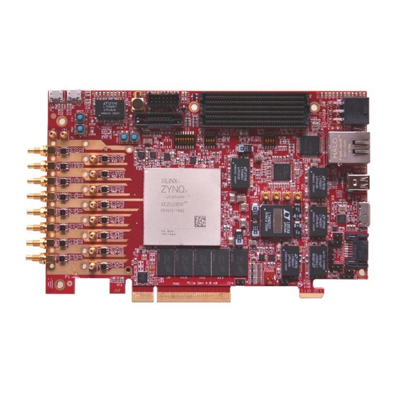
Page 5: Overview
(FMC+) port. The HTG-ZRF8 can host wide range of Vita57.1 /Vita57.4 compliant daughter cards. The HTG-ZRF8 is supported by one 72-bit ECC DDR4 SODIMM socket providing access to up to 16 GB of SDRAM memory. The processor’s side is supported by up to 2GB of DDR4 memory. -
Page 6: Features
Power adapter for standalone operation ◙ 3.0) Banks Assignment, Block Diagram, Clocks Diagram & Mechanical Drawing Figure (1) , (2), (3) and (4) illustrate FPGA I/O bank assignment, block diagram , clocks diagram, and mechanical dimensions of the HTG-ZRF8 platform. www.HiTechGlobal.com... -
Page 7: Figure (1): Fpga Bank Assignment
HTG-ZRF8 Platform User Manual Figure (1): FPGA Bank Assignment www.HiTechGlobal.com... -
Page 8: Figure (2): System Block Diagram
HTG-ZRF8 Platform User Manual Figure (2): System Block Diagram www.HiTechGlobal.com... -
Page 9: Figure (3): Clock Block Diagram
HTG-ZRF8 Platform User Manual Figure (3): Clock Block Diagram www.HiTechGlobal.com... -
Page 10: Figure (4): Mechanical Drawing
HTG-ZRF8 Platform User Manual Figure (4): Mechanical Drawing www.HiTechGlobal.com... -
Page 11: Main Clocks
HTG-ZRF8 Platform User Manual ◙ 4.0) Clocks The HTG-ZRF8 provides combination of fixed, programmable, and adjustable ultra-low-jitter clock sources for different interfaces as summarized by the table (2). Source Part Number (Manufacturer) Default Value Clock Function Si5341A Programmable User, DDR 4 , FMC+, Processor GTR & SMP SIT8103AC-23-18E-33.33333MHz... - Page 12 HTG-ZRF8 Platform User Manual Figure (5): Si5341 Clock Generator Block Diagram www.HiTechGlobal.com...
-
Page 13: Table (3): Summary Of The Si5341 (U46) Clock Outputs
HTG-ZRF8 Platform User Manual Table (3) provides summary of clock outputs of the Si5341 (U46) clock generator. FPGA Pin Output # Signal Name Destination Number OUT0_P CLK_PL_USER1_P FPGA Bank 87 (User Clock) OUT0_N CLK_PL_USER1_N SYS_CLK_DDR4_PL_P OUT1_P FPGA Bank67 (DDR4 SODIMM Clock) -
Page 14: Pci Express
Figure (6): LMX2592 Block Diagram ◙ 5.0) PCI Express The HTG-ZRF8 platform provides an 8-lane PCI Express Gen4 (8@16Gbps) end-point interface through integration of eight GTY serial transceivers (GTY 128 and 129) and one eight-lane hard-coded PCIe Link Layer Controller (X0Y0) of the FPGA. -
Page 15: Table (4): Pci Express Fpga Pin Assignments
Table (4): PCI Express FPGA Pin Assignments 5.1) PCI Express Clock The HTG-ZRF8 platform is supported by an auxiliary PCI Express jitter attenuator chip (871S1022EKLF) cleaning the 100MHz clock received by host PCs or servers. The jitter attenuator can also generate clock for the PCIe interface independent from host PCs or servers through its 25MHz (ZQ1) oscillator. -
Page 16: Table (5): Pci Express Clock Circuit
HTG-ZRF8 Platform User Manual Figure (7): PCI Express Clock Circuit PCI Express clock frequency value is set to 100 MHz by default. The output clock value can be adjusted by selecting N1:N0 attributes as shown by table (5) and figure (8). -
Page 17: Ddr 4 Memory
◙ 6.0) DDR-4 Memory The HTG-ZRF8 platform supports one DDR4 SODIMM socket providing access to up to 16GB of memory through the FPGA programmable logic and five DDR4 components providing access to 2GB of memory through the processor’s block of the FPGA. - Page 18 HTG-ZRF8 Platform User Manual DDR4_PL_A[16] DDR4_PL_ACT_N DDR4_PL_ALERT_N DDR4_PL_BA[0] DDR4_PL_BA[1] DDR4_PL_BG[0] DDR4_PL_BG[1] DDR4_PL_CK0_C DDR4_PL_CK0_T DDR4_PL_CK1_C DDR4_PL_CK1_T DDR4_PL_CKE0 DDR4_PL_CKE1 DDR4_PL_CS0_N DDR4_PL_CS1_N DDR4_PL_CS2_N DDR4_PL_CS3_N DDR4_PL_DM_DBI_N[0] DDR4_PL_DM_DBI_N[1] DDR4_PL_DM_DBI_N[2] DDR4_PL_DM_DBI_N[3] DDR4_PL_DM_DBI_N[4] DDR4_PL_DM_DBI_N[5] DDR4_PL_DM_DBI_N[6] DDR4_PL_DM_DBI_N[7] DDR4_PL_DM_DBI_N[8] DDR4_PL_DQ[0] DDR4_PL_DQ[1] DDR4_PL_DQ[2] DDR4_PL_DQ[3] DDR4_PL_DQ[4] DDR4_PL_DQ[5] DDR4_PL_DQ[6] DDR4_PL_DQ[7] DDR4_PL_DQ[8] DDR4_PL_DQ[9]...
- Page 19 HTG-ZRF8 Platform User Manual DDR4_PL_DQ[15] DDR4_PL_DQ[16] DDR4_PL_DQ[17] DDR4_PL_DQ[18] DDR4_PL_DQ[19] DDR4_PL_DQ[20] DDR4_PL_DQ[21] DDR4_PL_DQ[22] DDR4_PL_DQ[23] DDR4_PL_DQ[24] DDR4_PL_DQ[25] DDR4_PL_DQ[26] DDR4_PL_DQ[27] DDR4_PL_DQ[28] DDR4_PL_DQ[29] DDR4_PL_DQ[30] DDR4_PL_DQ[31] DDR4_PL_DQ[32] DDR4_PL_DQ[33] DDR4_PL_DQ[34] DDR4_PL_DQ[35] DDR4_PL_DQ[36] DDR4_PL_DQ[37] DDR4_PL_DQ[38] DDR4_PL_DQ[39] DDR4_PL_DQ[40] DDR4_PL_DQ[41] DDR4_PL_DQ[42] DDR4_PL_DQ[43] DDR4_PL_DQ[44] DDR4_PL_DQ[45] DDR4_PL_DQ[46] DDR4_PL_DQ[47] DDR4_PL_DQ[48] DDR4_PL_DQ[49] DDR4_PL_DQ[50]...
-
Page 20: Table (6): Ddr4 Fpga Pin Assignment (Sodimm-Pl Side)
HTG-ZRF8 Platform User Manual DDR4_PL_DQ[56] DDR4_PL_DQ[57] DDR4_PL_DQ[58] DDR4_PL_DQ[59] DDR4_PL_DQ[60] DDR4_PL_DQ[61] DDR4_PL_DQ[62] DDR4_PL_DQ[63] DDR4_PL_DQ[64] DDR4_PL_DQ[65] DDR4_PL_DQ[66] DDR4_PL_DQ[67] DDR4_PL_DQ[68] DDR4_PL_DQ[69] DDR4_PL_DQ[70] DDR4_PL_DQ[71] DDR4_PL_DQS_C[0] DDR4_PL_DQS_C[1] DDR4_PL_DQS_C[2] DDR4_PL_DQS_C[3] DDR4_PL_DQS_C[4] DDR4_PL_DQS_C[5] DDR4_PL_DQS_C[6] DDR4_PL_DQS_C[7] DDR4_PL_DQS_C[8] DDR4_PL_DQS_T[0] DDR4_PL_DQS_T[1] DDR4_PL_DQS_T[2] DDR4_PL_DQS_T[3] DDR4_PL_DQS_T[4] DDR4_PL_DQS_T[5] DDR4_PL_DQS_T[6] DDR4_PL_DQS_T[7] DDR4_PL_DQS_T[8] DDR4_PL_EVENT_N DDR4_PL_ODT0... - Page 21 HTG-ZRF8 Platform User Manual DDR4 Components Signal Name FPGA Pin Number DDR4_PS_A[0] AV31 DDR4_PS_A[1] AW28 DDR4_PS_A[2] AV28 DDR4_PS_A[3] AU29 DDR4_PS_A[4] AW31 DDR4_PS_A[5] AU28 DDR4_PS_A[6] AL29 DDR4_PS_A[7] AM30 DDR4_PS_A[8] AM29 DDR4_PS_A[9] AP29 DDR4_PS_A[10] AT31 DDR4_PS_A[11] AT32 DDR4_PS_A[12] AT30 DDR4_PS_A[13] AU32 DDR4_PS_A[14]...
- Page 22 HTG-ZRF8 Platform User Manual DDR4_PS_DQ[5] AV22 DDR4_PS_DQ[6] AR24 DDR4_PS_DQ[7] AR23 DDR4_PS_DQ[8] AT25 DDR4_PS_DQ[9] AP26 DDR4_PS_DQ[10] AU25 DDR4_PS_DQ[11] AR27 DDR4_PS_DQ[12] AU27 DDR4_PS_DQ[13] AV26 DDR4_PS_DQ[14] AV27 DDR4_PS_DQ[15] AW26 DDR4_PS_DQ[16] AP25 DDR4_PS_DQ[17] AP24 DDR4_PS_DQ[18] AP23 DDR4_PS_DQ[19] AN25 DDR4_PS_DQ[20] AM25 DDR4_PS_DQ[21] AK24 DDR4_PS_DQ[22] AN23...
- Page 23 HTG-ZRF8 Platform User Manual DDR4_PS_DQ[46] AP33 DDR4_PS_DQ[47] AP34 DDR4_PS_DQ[48] AL39 DDR4_PS_DQ[49] AM38 DDR4_PS_DQ[50] AM39 DDR4_PS_DQ[51] AN38 DDR4_PS_DQ[52] AM35 DDR4_PS_DQ[53] AM34 DDR4_PS_DQ[54] AN36 DDR4_PS_DQ[55] AN35 DDR4_PS_DQ[56] AK32 DDR4_PS_DQ[57] AK31 DDR4_PS_DQ[58] AJ31 DDR4_PS_DQ[59] AJ30 DDR4_PS_DQ[60] AH30 DDR4_PS_DQ[61] AG32 DDR4_PS_DQ[62] AF32 DDR4_PS_DQ[63] AG30...
-
Page 24: Fpga Mezzanine Card (Fmc+)
◙ 7.0) FPGA Mezzanine Card (FMC+) Interface (Vita57.4) The HTG-ZRF8 platform is populated with one Vita57.4 compliant FMC+ connector with 68 single-ended I/Os and 8 GTY (32.75Gbps) Serial Transceivers. This expansion port hosts Vita57.1 or Vita57.4 compliant daughter cards. HiTech Global offers wide range of add-on FMC and FMC+ modules as shown on http://www.hitechglobal.com/Accessories/FMC_Modules.htm... -
Page 25: Table (8): Vita57.4 Fmc+ Pin Assignment
HTG-ZRF8 Platform User Manual Table (8): Vita57.4 FMC+ Pin Assignment www.HiTechGlobal.com... - Page 26 HTG-ZRF8 Platform User Manual Table (9) illustrates FPGA pin assignment for the PL side FMC+ interface. FMC+ Signal Name FPGA Pin Number FMC_PL_CLK[0]_M2C_ AP21 FMC_PL_CLK[0]_M2C_ AN21 FMC_PL_DP[0]_C2M_N FMC_PL_DP[0]_C2M_P FMC_PL_DP[0]_M2C_N FMC_PL_DP[0]_M2C_P FMC_PL_DP[1]_C2M_N FMC_PL_DP[1]_C2M_P FMC_PL_DP[1]_M2C_N FMC_PL_DP[1]_M2C_P FMC_PL_DP[2]_C2M_N FMC_PL_DP[2]_C2M_P FMC_PL_DP[2]_M2C_N FMC_PL_DP[2]_M2C_P FMC_PL_DP[3]_C2M_N FMC_PL_DP[3]_C2M_P...
- Page 27 HTG-ZRF8 Platform User Manual FMC_PL_LA[0]_CC_N AR18 FMC_PL_LA[0]_CC_P AP18 FMC_PL_LA[1]_CC_N AN20 FMC_PL_LA[1]_CC_P AM20 FMC_PL_LA[2]_N AT22 FMC_PL_LA[2]_P AR22 FMC_PL_LA[3]_N AT21 FMC_PL_LA[3]_P AR21 FMC_PL_LA[4]_N AW21 FMC_PL_LA[4]_P AV21 FMC_PL_LA[5]_N AK21 FMC_PL_LA[5]_P AK22 FMC_PL_LA[6]_N AV18 FMC_PL_LA[6]_P AU18 FMC_PL_LA[7]_N AL20 FMC_PL_LA[7]_P AL21 FMC_PL_LA[8]_N AM22 FMC_PL_LA[8]_P AL22...
-
Page 28: Table (9): Fpga Mezzanine Connector (Fmc+) Pin Assignment
HTG-ZRF8 Platform User Manual FMC_PL_LA[20]_P FMC_PL_LA[21]_N AN13 FMC_PL_LA[21]_P AM13 FMC_PL_LA[22]_N AU10 FMC_PL_LA[22]_P AT10 FMC_PL_LA[23]_N AW11 FMC_PL_LA[23]_P AV11 FMC_PL_LA[24]_N FMC_PL_LA[24]_P FMC_PL_LA[25]_N AM14 FMC_PL_LA[25]_P AL14 FMC_PL_LA[26]_N AN12 FMC_PL_LA[26]_P AM12 FMC_PL_LA[27]_N AR11 FMC_PL_LA[27]_P AR12 FMC_PL_LA[28]_N AM10 FMC_PL_LA[28]_P AL10 FMC_PL_LA[29]_N AK14 FMC_PL_LA[29]_P AJ14 FMC_PL_LA[30]_N... -
Page 29: Table (10): Rfb Resistor Table Vs Various Output Voltages
HTG-ZRF8 Platform User Manual 7.1) FMC+ Clock Clocks for the FMC+ I/Os are generated by the onboard Si5341 programmable clock generator through OUT2 (FMC_PL_REFCLK_C2M) , OUT3 (GTY_131_REFCLK) and OUT4 (GTY_130_REFCLK) ports as shown by figure (5) and table (3). 7.2) FMC VADJ V_Adjust carries an adjustable voltage level power from the FPGA carrier board to the I/O Mezzanine modules. -
Page 30: Adc / Dac Ports
HTG-ZRF8 Platform User Manual ◙ 8.0) ADC and DAC Ports The HTG-ZRF platform provides access to eight 12-bit ADC (4GSPS) and eight 14-bit DAC (6.4GSPS) ports through sixteen SSMC connectors. The ADC and DAC ports are supported through high-performance front panel Mini Circuits TCM1-83X+ micro Rf connectors (with bandwidth from 10 to 8000 MHz). -
Page 31: Table (12): Dac Interface Pin Assignment
HTG-ZRF8 Platform User Manual DAC_229_REFCLK_P U66 Clock Fanout (Q2-P) DAC_VOUT0_228_N J16 SSMC / Rf Transformer DAC_VOUT0_228_P J16 SSMC / Rf Transformer DAC_VOUT0_229_N J14 SSMC / Rf Transformer DAC_VOUT0_229_P J14 SSMC / Rf Transformer DAC_VOUT1_228_N J6 SSMC / Rf Transformer DAC_VOUT1_228_P... -
Page 32: Usb To Uart Bridges
9.0) USB To UART Bridges The HTG-ZRF8 platform provides access to two UART ports for the PL and PS sides through two peripheral USB connectors (J1 and J12). These ports are supported by the Silicon labs CP2103 USB to UART controller chips (U70 and U71). -
Page 33: Arm Trace Port
◙ 10.0) ARM Trace Port The HTG-ZRF8 provides access to one standard ARM Trace/Debug port (38-pin Mictor connector). The pin out follows the single target connector pinout specification as defined in the ARM "Architecture Specification. Table (14) illustrates FPGA pin assignment for the ARM Trace/Debug port (J22) -
Page 34: Sdio Interface
◙ 11.0) SDIO Interface The HTG-ZRF8 supports a secure digital input/output (SDIO) interface providing access to general purpose non-volatile SDIO memory cards and peripherals. The SDIO signals are connected to the PS bank 501 of the onboard Zynq UltraScale+ FPGA. A SD 2.0-compliant voltage level-translator (SN74AVCA406EZQS) is present between the onboard Zynq UltraScale+ RFSoC FPGA and the SD card connector (J35). -
Page 35: 10/100/1000 Ethernet
◙ 12.0) 10/100/1000 Mbps Ethernet The HTG-ZRF8 platform provides access to one 10/100/1000 Mbps Ethernet port (J30) supported by Texas Instruments DP83867IRPAP PHY chip connected to the processor’s I/Os of the FPGA. The DP83867 device is a fully featured Physical Layer transceiver with integrated PMD sublayers to support 10BASE-Te, 100BASE-TX and 1000BASE-T Ethernet protocols. -
Page 36: Display Port
◙ 14.0) USB 2.0/3.0 The HTG-ZRF8 platform provides access to a USB 2.0 through Microchip USB3320 chip and USB 3.0 through GTR serial transceivers of the FPGA’s processor side. The Microchip USB3320 is a USB 2.0 Transceiver that provides a configurable physical layer (PHY). The USB3320 meets all of the electrical requirements to be used as a Hi-Speed USB Host, Device, or an On-the-Go (OTG) transceiver. -
Page 37: Sata
◙ 15.0) SATA The HTG-ZRF8 platform provides access to one Serial ATA port (J33). The port can be used for standard SATA storage access applications or board-to-board connection. Reference clock for the SATA serial transceivers is provided by the onboard SI5341 clock generator (U19). -
Page 38: Leds, Xdac, User I/O Headers & Pushbutton
◙ 18.0) IP Protection The HTG-ZRF8 platform provides access to a special circuit (U7) for protection of intellectual properties loaded to the FPGA (pin # A9) by using Maxim DS2432 chip. The DS2432 combines 1024 bits of EEPROM, a 64-bit secret, an 8-byte register/control page with up to five user read/write bytes, a 512-bit SHA-1 engine, and a fully-featured 1-Wire interface in a single chip. -
Page 39: I2C Bus Switch
◙ 19.0) I2C Bus Switch All I2C-controlled devices on the HTG-ZRF8 platform are controlled by the FPGA Logic or/and the processor signals and the I2C Bus Switch chip (U51) as shown by the below FPGA signals and figure (12) I2C_RST_N_PL... -
Page 40: Configuration
Figure (12): I2C Bus Switch ◙ 20.0) Configuration The HTG-ZRF8 can be configured using its Jtag, QSPI, or MicroSD port. Quad-SPI Booting from the dual Quad-SPI nonvolatile configuration memory is accomplished by storing a valid Zynq UltraScale+ MPSoC boot image (.MCS) into the Quad-SPI flash devices connected to the MIO Quad-SPI... -
Page 41: Figure (13): Configuration Option
HTG-ZRF8 Platform User Manual Figure (13): Configuration Option www.HiTechGlobal.com...
Need help?
Do you have a question about the HTG-ZRF8 and is the answer not in the manual?
Questions and answers