
Summary of Contents for Bitwise QuickUSB
- Page 1 User Guide 6489 Calle Real, Suite E Goleta, CA 93117 Voice (805) 683-6469 (805) 683-4833 Toll Free (800) 224-1633 Web Site www.bitwisesys.com Information info@bitwisesys.com Technical Support support@bitwisesys.com...
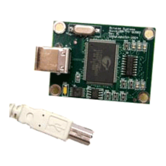
- Page 2 QuickUSB User Guide Version 2.11.35 April 28, 2006 Copyright © 2005, 2006 Bitwise Systems. All rights reserved. This document contains confidential information and trade secrets of Bitwise Systems, and is protected by United States and international copyright laws. Use, disclosure, or reproduction is prohibited without the prior express written permission of Bitwise Systems, except as agreed in the License Agreement.
-
Page 3: Table Of Contents
Table of Contents Introduction QuickUSB and the Big USB Picture USB Nomenclature USB System Architecture I/O Subsystem Latency and Throughput USB Interpacket Delay Designing Hardware for QuickUSB The Cypress EZ USB FX2 Power and Ground Unused I/O Pins DefaultI/O State... - Page 4 QuickUsbWriteFpgaData QuickUsbIsFpgaConfigured High-Speed Parallel Port QuickUsbReadCommand QuickUsbWriteCommand QuickUsbReadData QuickUsbWriteData QuickUsbReadDataAsync QuickUsbWriteDataAsync QuickUsbAsyncWait General-Purpose I/O QuickUsbReadPortDir QuickUsbWritePortDir QuickUsbReadPort QuickUsbWritePort RS-232 QuickUsbSetRs232BaudRate QuickUsbGetNumRS232 QuickUsbFlushRS232 QuickUsbReadRS232 QuickUsbWriteRS232 I2C-Compatible Port QuickUsbReadI2c QuickUsbWriteI2c SPI-Compatible Port QuickUsbReadSpi QuickUsbWriteSpi QuickUsbWriteReadSpi Index...
-
Page 5: Introduction
Part of that design defines the relationship between your PC and the device. Although with QuickUSB you do not need to learn the inner workings of USB, you do need to understand the basics of USB. We will explain the basics here and if you want to learn more, you can browse www.usb.org... -
Page 6: I/O Subsystem Latency And Throughput
QuickUSB and the Big USB Picture I/O Subsystem Latency and Throughput The period of time between the start of a transfer and the time that it actually occurs is the transfer latency. USB transfer latency is the result of several factors. -
Page 7: Designing Hardware For Quickusb
Power and Ground QuickUSB supplies unregulated +5V at up to 400 mA max on the VBUS pins to power your circuitry. For modules Rev A1 and above, an FET on the QuickUSB module controls power. Power is off by default and then turned on once the host configures the module. -
Page 8: Unused I/O Pins
Some I/O pins are reserved for future use and may be activated by a new version of the module or a new firmware release. Therefore, you must not connect unused QuickUSB I/O pins to any signals or power supplies. DO NOT DIRECTLY GROUND UNUSED QUICKUSB I/O PINS IN YOUR CIRCUIT. You may use a 10k resistor to tie unused pins to a known level, but do not connect them directly. -
Page 9: Gpif Master Mode
Designing Hardware for QuickUSB GPIF Master Mode In GPIF master mode, the QuickUSB module controls all aspects of the HSPP and the host PC initiates all data transfers through the QuickUSB module. This mode is implemented using the GPIF programmable DMA engine built into the FX2. -
Page 10: Gpif Master Mode I/O Models
Designing Hardware for QuickUSB GPIF Master Mode I/O Models The QuickUSB module interfaces to target hardware by implementing a number of I/O models that provide enough flexibility to interface to a wide variety target hardware. The I/O models are selected by reprogramming the firmware of the QuickUSB module using the QuickUSB Programmer. - Page 11 This I/O model performs transfers without regard to the readiness of the target hardware. This model is suitable for hardware that is always ready and that can transfer data as fast as the host can deliver it. This is the fastest QuickUSB I/O model available.
- Page 12 RDY0 nFULL RDY1 Signifies QuickUSB Read from the Data Bus Full Speed, Byte Wide: N = 63 High Speed, Byte Wide: N = 511 Full Speed, Word Wide: N = 31 High Speed, Word Wide : N = 255...
- Page 13 Designing Hardware for QuickUSB FIFO Handshake I/O Model This I/O model is designed specifically to allow QuickUSB to connect directly to external synchronous or asynchronous FIFOs. This I/O model is ideal for applications that combine QuickUSB with FPGA. QuickUsbRead/WriteData functions read or write streaming data to FIFOs inside the FPGA while the QuickUsbRead/WriteCommand functions control a register array inside the FPGA to manage internal FPGA operations.
- Page 14 CTL5 nEMPTY RDY0 nFULL RDY1 Signifies QuickUSB Read from the Data Bus Full Speed, Byte Wide: N = 63 High Speed, Byte Wide: N = 511 Full Speed, Word Wide: N = 31 High Speed, Word Wide: N=255 Write Cycle...
- Page 15 This model implemented QuickUSB firmware file ‘quickusb-fullhs vX.XX.qusb’ where X.XX is the firmware version number. Command Transfers Read Cycle Write Cycle XCTL XCTL XCTL XCTL...
- Page 16 QuickUSB firmware file ‘quickusb-blockhs vX.XX.qusb’ where X.XX is the firmware version number. The Block I/O model is designed to provide the highest possible data rate possible with hardware handshaking. AS A RESULT, THERE ARE CERTAIN INVALID TRANSFER LENGTHS THAT MAY RESULT IN A FATAL SOFTWARE ERROR WHICH MAY CRASH YOUR COMPUTER.
- Page 17 CTL5 nEMPTY RDY0 nFULL RDY1 Signifies QuickUSB Read from the Data Bus Full Speed, Byte Wide: N = 63 High Speed, Byte Wide: N = 511 Full Speed, Word Wide: N = 31 High Speed, Word Wide: N = 255...
- Page 18 QuickUSB firmware file ‘quickusb-pipe1 vX.XX.qusb’ where X.XX is the firmware version number. The Pipeline I/O model is designed to provide the highest possible data rate possible with hardware handshaking. AS A RESULT, THERE ARE CERTAIN INVALID TRANSFER LENGTHS THAT MAY RESULT IN A FATAL SOFTWARE ERROR WHICH MAY CRASH YOUR COMPUTER.
- Page 19 CTL5 nEMPTY RDY0 nFULL RDY1 Signifies QuickUSB Read from the Data Bus Full Speed, Byte Wide: N = 63 High Speed, Byte Wide: N = 511 Full Speed, Word Wide: N = 31 High Speed, Word Wide: N=255 Write Cycle...
-
Page 20: Slave Fifo I/O Models
Slave FIFO mode is selected by changing Bits1-0 of the SETTING_FIFO_CONFIG setting and may be changed at any time. In slave FIFO mode, data is transferred to and from the QuickUSB FIFOs using the standard QuickUsbReadData (EP6) &... - Page 21 … Data[N] Data[N-1 FIFOADR[1:0] PA5:PA4 nSLRD RDY0 nSLWR RDY1 FLAGB (nFULL) CTL1 FLAGC (nEMPTY) CTL2 nSLOE nPKTEND nSLCS Signifies QuickUSB Write to the Data Bus Write Cycle FAFLG FAFLG XFLG IFCLK Name IFCLK IFCLK DATA Data0 Data1 Data2 Data3 Data4 …...
- Page 22 Designing Hardware for QuickUSB Internally Externally Parameter Description Sourced IFCLK Sourced IFCLK Unit tIFCLK IFCLK Period 20.83 20.83 200 ns tSRD SLRD to Clock Set-up 18.7 12.7 Time tRDH Clock to SLRD Hold Time tOEon SLOE Turn-on to FIFO 10.5 10.5 ns...
- Page 23 Data0 Data1 Data2 FIFOADR[1:0] PA5:PA4 nSLRD RDY0 nSLWR RDY1 nSLOE FLAGB (nFULL) CTL1 FLAGC (nEMPTY) CTL2 nPKTEND nSLCS Signifies QuickUSB Read from the Data Bus Read Cycle RDpwl XFLG RDpwh XFDRD OEoff OEon XFLG Name DATA Data0 Data1 Data2 FIFOADR[1:0]...
- Page 24 Designing Hardware for QuickUSB Slave245 I/O Model The Slave245 I/O Model allows QuickUSB to duplicate the functionality of the FTDI245BM I/O waveforms with a speed increase of up to 10X. This I/O model is implemented in the QuickUSB firmware file ‘quickusb-245 vX.XX.qusb’ where X.XX is the firmware version number.
-
Page 25: Fpga Configuration
Currently, two configuration schemes are supported: Altera Passive Serial and Xilinx Slave Serial. The QuickUSB module uses 3.3V I/O, so make sure your device can handle 3.3V on the configuration pins. Then, connect the FPGA as shown in Table 6. You must be sure to add pull-up resistors required by the FPGA manufacturer. -
Page 26: Spi
Designing Hardware for QuickUSB The QuickUSB module implements a ‘soft’ SPI port using pins on port E and optionally port A. These routines support from 1 to 10 devices with individual slave select lines for each device. The slave select lines are active low and are... -
Page 27: Quickusb Pin Definitions
QUSB2 Name Desc Function SW_EN Output VBUS Switch SW_EN is high when the QuickUSB Enable Module has successfully enumerated and power can be drawn from VBUS. Used to control the VBUS switch on the QuickUSB Module. PA0 / Port A, Bit 0... - Page 28 Designing Hardware for QuickUSB FX2128 QUSB2 Name Desc Function PA4 / nSS6/ Port A, Bit 4 Multifunction Pin whose function is FIFOADR0 selected by SETTING_FIFO_CONFIG[1:0]: PA4 (default) is a bi-directional general purpose I/O pin. Enabled when SETTING_FIFO_CONFIG[1:0]: = '00' or '10' nSS6 is the SPI slave select signal for Address 6.
- Page 29 Designing Hardware for QuickUSB FX2128 QUSB2 Name Desc Function PA7 / nSS9 Port A, Bit 7 Multifunction Pin whose function is / FLAGD / selected by nSLCS SETTING_FIFO_CONFIG[1:0]: PA7 (default) is a bi-directional general purpose I/O pin. Enabled when SETTING_FIFO_CONFIG[1:0]...
- Page 30 Designing Hardware for QuickUSB FX2128 QUSB2 Name Desc Function PB4 / FD4 Port B, Bit 4 Multifunction Pin whose function is selected by SETTING_FIFO_CONFIG[1:0]: PB4 is a bi-directional general purpose I/O port. Enabled when SETTING_FIFO_CONFIG[1:0] ='00' FD4 (default) is the bi-directional GPIF data bus low byte.
- Page 31 Designing Hardware for QuickUSB FX2128 QUSB2 Name Desc Function PC2 / Port C, Bit 2 Multifunction Pin whose function is GPIFADR2 selected by SETTING_FIFO_CONFIG[1:0]: PC2 is a bi-directional general purpose I/O port. Enabled when SETTING_FIFO_CONFIG[1:0] ='00' GPIFADR2 (default) is a GPIF address output pin.
- Page 32 Designing Hardware for QuickUSB FX2128 QUSB2 Name Desc Function PD0 / FD8 Port D, Bit 0 Multifunction Pin whose function is selected by SETTING_FIFO_CONFIG[1:0]: PD0 is a bi-directional general purpose I/O port. Enabled when SETTING_FIFO_CONFIG[1:0] ='00' or when SETTING_WORDWIDE = '0' FD8 (default) is the bi-directional GPIF data bus.
- Page 33 Designing Hardware for QuickUSB FX2128 QUSB2 Name Desc Function PD4 / FD12 Port D, Bit 4 Multifunction Pin whose function is selected by SETTING_FIFO_CONFIG[1:0]: PD4 is a bi-directional general purpose I/O port. Enabled when SETTING_FIFO_CONFIG[1:0] ='00' or when SETTING_WORDWIDE = '0' FD12 (default) is the bi-directional GPIF data bus.
- Page 34 Designing Hardware for QuickUSB FX2128 QUSB2 Name Desc Function PE0 / Port E, Bit 0 Multifunction Pin DATA0 / PE0 (default) is a bi-directional MOSI general purpose I/O port. Enabled when SETTING_FIFO_CONFIG[1:0] ='00', '10', or '11' DATA0 is the data output signal for serial FPGA configuration.
- Page 35 Designing Hardware for QuickUSB FX2128 QUSB2 Name Desc Function PE5 / Port E, Bit 5 Multifunction Pin CONF_DO PE5 (default) is a bi-directional NE / MISO general purpose I/O port. Enabled when SETTING_FIFO_CONFIG[1:0] ='00', '10', or '11' CONF_DONE is the Done output signal for serial FPGA configuration.
- Page 36 Serial Port 0 Serial Port 0 RxD Note: If U1 is populated with a Linear Tech part, QuickUSB Module uses EIA/TIA 564 Levels. If U1 is populated with a TI part, QuickUSB Module uses RS-232 levels. TXD_0 Output Serial Port 0...
- Page 37 Designing Hardware for QuickUSB FX2128 QUSB2 Name Desc Function CTL1 / REN Output GPIF Control Multifunction Pin whose function is / FLAGB / Output 1 selected by nFULL SETTING_FIFO_CONFIG[1:0]: CTL1 (default) is a GPIF output signal whose function (REN) is waveform specific.
- Page 38 Designing Hardware for QuickUSB FX2128 QUSB2 Name Desc Function CTL4 / Output GPIF Control CTL4 is a GPIF output signal whose nWEN Output 4 function (nWEN) is waveform specific. Enabled when SETTING_FIFO_CONFIG[1:0] = '10'. nWEN is the active low Write Enable output signal for the GPIF.
- Page 39 Designing Hardware for QuickUSB FX2128 QUSB2 Name Desc Function RDY0 / Input GPIF input Multifunction Pin whose function is nEMPTY / signal 0 selected by READY / SETTING_FIFO_CONFIG[1:0]: nSLRD RDY0 (default) is a GPIF input signal whose function (nEMPTY or READY) is waveform specific.
- Page 40 Function WAKEUP_ Input USB Wakeup USB Wakeup. Asserting pin brings FX2 out of suspend mode. Active Low. Not used, connected to VCC through a 10k resistor on QuickUSB Module. DMINUS USB D- Connect to the USB D- Signal Signal DPLUS...
- Page 41 Designing Hardware for QuickUSB FX2128 QUSB2 Name Desc Function Output External External Memory Write Strobe. Active Memory Write Low. Not connected on QuickUSB Strobe Module Output External External Memory Read Strobe. Active Memory Read Low. Not connected on QuickUSB Strobe Module...
- Page 42 Name Desc Function Ground Ground Ground Ground No Connect This pin must be left open. No Connect This pin must be left open. No Connect This pin must be left open. Table 7 - QuickUSB Pin Definitions QuickUSB Pin Definitions...
-
Page 43: Using The Quickusb Library
The QuickUSB® Library API gives programmers a cohesive programming interface to the QuickUSB family of products. The same QuickUSB Library API works for all QuickUSB products on all platforms, so you write your software once and all your QuickUSB based products will work on any supported platform. -
Page 44: System Considerations
HANDLE a LONG PHANDLE a pointer to a HANDLE Blocking versus Non-blocking Data Transfers The QuickUSB Library allows a user to make both Blocking (QuickUsbReadData and QuickUsbWriteData) and Non-blocking (QuickUsbReadDataAsync and QuickUsbWriteDataAsync) data transfer calls. When called, the Blocking functions will initiate a data transfer, and will return from the function once that data transfer has completed. -
Page 45: Quickusb Base Api
Build a list of all QuickUSB modules connected to the host. Parameters nameList: A PCHAR that points to a buffer in which to store a of QuickUSB module names found by the library. Device names are of the form ‘QUSB-XXX’ where XXX is the device address (0-126) in decimal. -
Page 46: Quickusbclose
A LONG that is either non-zero on success or zero (0) on failure. Notes None. QuickUsbGetStringDescriptor Purpose Returns the string descriptor for the selected QuickUSB module. Parameters hDevice: A HANDLE that was returned from a call to QuickUsbOpen. index: The BYTE string descriptor index given in the following table:... -
Page 47: Quickusbsettimeout
Using the QuickUSB Library QuickUsbSetTimeout Purpose Set the timeout for QuickUSB read data transfers. Parameters hDevice: A HANDLE that was returned from a call to QuickUsbOpen. timeout: A LONG that specifies the new timeout value in milliseconds. Returns A LONG that is either non-zero on success or zero (0) on failure. -
Page 48: Quickusbgetfirmwareversion
Timeout occurred while attempting to read or write data. This function is not supported by the version of the QuickUSB driver you are using. Please update your driver to the latest version. I2C bus error. -
Page 49: Quickusb Settings
Using the QuickUSB Library QuickUSB Settings The QuickUSB module has certain settings that control the behavior of the module. These functions manipulate those settings in order to customize the module’s behavior for your particular needs. A list of settings follows:... - Page 50 Using the QuickUSB Library Addr Name Description Values SETTING_WORDWIDE High-speed port data width MSB=Unused, Reserved for future use. LSB - Bit definitions: Bit 7-1: Reserved Bit 0: WORDWIDE – HSPP data width 0 = 8 bits 1 = 16 bits...
- Page 51 Using the QuickUSB Library Addr Name Description Values 0=Normal 1=Inverted Bit 3: ASYNC – GPIF clock mode select 0=Synchronous GPIF 1=Asynchronous GPIF Bit 2: Reserved (do not change) Bit 1-0: IFCFG- HSPP Configuration 00=I/O ports 01=Reserved 10=GPIF Master mode 11=Slave FIFO mode...
- Page 52 Using the QuickUSB Library Addr Name Description Values SETTING_SLAVEFIFOFLAG Returns Slave FIFO flag Bit 15-12: Reserved for future use status. Bit 11: RDY0 Pin Status Note: These flags are only Bit 10: Reserved for future use significant when the FX2 is Bit 9: Empty Flag for EP6 in slave FIFO mode.
- Page 53 Using the QuickUSB Library Addr Name Description Values SETTING_PORTC Configures Port C default MSB = OEC – Port C Output state. Reading a bit from Enable Bit Definitions IOC returns the logic level 0 = Disables output buffer of the port pin that is two 1 = Enables output buffer CLKOUT-clocks old.
- Page 54 Using the QuickUSB Library Addr Name Description Values input 0 = PA1 not configured as interrupt input (default) Note: INT1 is not currently used Bit 8: INT0 – Interrupt 0 Alternate Configuration 1 = PA0 configured as interrupt input 0 = PA0 not configured as...
-
Page 55: Quickusbreadsetting
LSB= USB bus speed Bit 7: 0=Full Speed (12Mbps) 1=High Speed (480Mbps) Bit 6-0: Reserved for future use Table 10 - QuickUSB Settings QuickUsbReadSetting Purpose To read QuickUSB module settings. Parameters hDevice: A HANDLE that was returned from a call to QuickUsbOpen. -
Page 56: Quickusbreaddefault
Using the QuickUSB Library QuickUsbReadDefault Purpose To read QuickUSB module defaults. The defaults are non-volatile and are read into the settings table on power up. Parameters hDevice: A HANDLE that was returned from a call to QuickUsbOpen. address: A WORD containing the default address (number) -
Page 57: Fpga Configuration
You must convert your FPGA configuration file to binary image format for use with QuickUSB. Altera binary files are of type RBF and Xilinx are of type BIT. If you are configuring multiple devices, they must be daisy-chained and the configuration files combined in the conversion process into a single binary file. -
Page 58: Quickusbwritefpgadata
Using the QuickUSB Library QuickUsbWriteFpgaData Purpose Sends FPGA configuration data to the FPGA using the QuickUSB FPGA configuration port. Parameters hDevice: A HANDLE that was returned from a call to QuickUsbOpen. data: A PBYTE pointing to a BYTE buffer containing the FPGA configuration data. -
Page 59: High-Speed Parallel Port
Using the QuickUSB Library High-Speed Parallel Port QuickUsbReadCommand Purpose Read a block of command values from the high-speed parallel port using the QuickUSB module. Parameters hDevice: A HANDLE that was returned from a call to QuickUsbOpen. address: A WORD containing the address. This address is the starting value of the HSPP address bus. -
Page 60: Quickusbwritecommand
Using the QuickUSB Library QuickUsbWriteCommand Purpose Write a block of command values to the high-speed parallel port using the QuickUSB module. Parameters hDevice: A HANDLE that was returned from a call to QuickUsbOpen. address: A WORD containing the address. This address is the starting value of the HSPP address bus. -
Page 61: Quickusbreaddata
Using the QuickUSB Library QuickUsbReadData Purpose Read a block of data values from the high-speed parallel port using the QuickUSB module. Parameters hDevice: A HANDLE that was returned from a call to QuickUsbOpen. data: A pointer to a buffer in which to place data values read from the HSPP. -
Page 62: Quickusbwritedata
Using the QuickUSB Library QuickUsbWriteData Purpose Write a block of data values to the high-speed parallel port using the QuickUSB module. Parameters hDevice: A HANDLE that was returned from a call to QuickUsbOpen. data: A pointer to a block of data values to write to the HSPP. See notes. -
Page 63: Quickusbreaddataasync
The address bus behavior for data transfers is defined by the SETTING_DATAADDRESS setting. • There is a global maximum of 253 asynchronous reads and writes outstanding at any time for all QuickUSB modules in the system. • This function is not yet supported for Linux-based systems. High-Speed Parallel Port... -
Page 64: Quickusbwritedataasync
The address bus behavior for data transfers is defined by the SETTING_DATAADDRESS setting. • There is a global maximum of 253 asynchronous reads and writes outstanding at any time for all QuickUSB modules in the system. • This function is not yet supported for Linux-based systems. High-Speed Parallel Port... -
Page 65: Quickusbasyncwait
Using the QuickUSB Library QuickUsbAsyncWait Purpose Wait for an asynchronous transfer to complete. Parameters hDevice: A HANDLE that was returned from a call to QuickUsbOpen. length: An ULONG containing the number of bytes that were requested in the initial asynchronous function call. -
Page 66: General-Purpose I/O
Using the QuickUSB Library General-Purpose I/O There are five (5) 8-bit general-purpose I/O ports on the QuickUSB module named A-E. Of those, some may be used for other purposes. Port E is used for the FPGA configuration and SPI functions, so if either of these functions is used in your design, some of the pins on port E will be consumed. -
Page 67: Quickusbreadport
Using the QuickUSB Library QuickUsbReadPort Purpose Read a series of bytes from the specified port. Parameters hDevice: A HANDLE that was returned from a call to QuickUsbOpen. address: The port address. Ports are addressed 0 to 4 corresponding to port A-E. -
Page 68: Rs-232
Using the QuickUSB Library RS-232 The RS-232 ports are interrupt-driven for transmit and receive. The QuickUSB RS232 receive buffers are 128 bytes deep, so your software just needs to service these buffers often enough to make sure they do not overflow. -
Page 69: Quickusbflushrs232
Using the QuickUSB Library QuickUsbFlushRS232 Purpose Flush the RS232 port transmit and receive buffers. Parameters hDevice: A HANDLE that was returned from a call to QuickUsbOpen. portNum: The serial port number. Serial port 0 (P1) = 0, serial port 1 (P2) = 1. -
Page 70: Quickusbwriters232
Using the QuickUSB Library QuickUsbWriteRS232 Purpose Write a block of characters to the specified QuickUSB serial port. Parameters hDevice: A HANDLE that was returned from a call to QuickUsbOpen. portNum: The serial port number. Serial port 0 (P1) = 0, serial port 1 (P2) = 1. -
Page 71: I2C-Compatible Port
Using the QuickUSB Library I2C-Compatible Port The QuickUSB I C-compatible port is a master-only bus controller. The bus runs at approximately 100Khz. Address 1 is reserved. The bus speed may be changed with the SETTING_I2CTL setting. QuickUsbReadI2c Purpose None Parameters hDevice: A HANDLE that was returned from a call to QuickUsbOpen. -
Page 72: Spi-Compatible Port
Using the QuickUSB Library SPI-Compatible Port The QuickUSB module implements a ‘soft’ SPI port using pins on port E and optionally port A. These routines support from 1 to 10 devices with individual slave select lines for each device. The slave select lines are active low and are... -
Page 73: Quickusbwritereadspi
Using the QuickUSB Library QuickUsbWriteReadSpi Purpose Simultaneously write and read a block of data to and from the specified SPI slave port. Parameters hDevice: A HANDLE that was returned from a call to QuickUsbOpen. portNum: The SPI device address (nSS line) to write to and read from... -
Page 74: Index
Index Index address bus ........4 unused ........4 architecture........1 IFCLK ..........5 ASYNC..........19 interpacket delay......2 asynchronous function calls ..2 interrupt .........1 latency..........2 address........4 master ..........1 high-speed parallel....4 mode CMD_DATA ........5 GPIF master ......5 current limiting......3 OE 5 defaults pipe..........1...
Need help?
Do you have a question about the QuickUSB and is the answer not in the manual?
Questions and answers