Table of Contents
Advertisement
Quick Links
The AK4458 is a 32-bit 8ch Premium DAC, which achieves industry's best low distortion characteristics by a
newly developed low distortion technology. It corresponds to a 768kHz PCM input and an 11.2MHz DSD
input at maximum, suitable for play backing high resolution audio sources that are becoming widespread in
network audios, USB-DACs and Car Audio Systems. In addition, "OSR-Doubler" technology is newly
adopted, making the AK4458 capable of supporting wide range signals and achieving low out-of-band noise
while realizing low power consumption. Moreover, the AK4458 has five types of 32-bit digital filters,
realizing simple and flexible sound making in wide range of applications.
Application: AV Receivers, CD/SACD Players, Network Audios, USB DACs, USB Headphones, Sound
Plate/Bars, Car Audios, Automotive External Amplifiers, Measuring Instruments and Control
Systems.
(1) DR, S/N: 115dB
(2) THD+N: -107dB
(3) 256x Over sampling (OSR - Doubler)
(4) Sampling Rate: 8kHz 768kHz
(5) 32Bit 8x Digital Filter
- Ripple: 0.0032dB, Attenuation: 80dB (Sharp Roll-Off Filter Setting)
- Five Types of High Quality Sound Filter Option
- Sharp Roll-Off Filter
- Slow Roll-Off Filter
- Short Delay Sharp Roll-Off Filter (GD=5.8/fs)
- Short Delay Slow Roll-Off Filter (GD=4.8/fs)
- Super Slow Roll-Off Filter
(6) High Tolerance to Clock Jitter
(7) Low Distortion Differential Output
(8) DSD data input
(9) Daisy Chain
(10) Digital De-emphasis for 32, 44.1, 48kHz sampling
(11) Soft Mute
(12) Digital Attenuator (255 levels and 0.5dB step)
(13) I/F Format:
- 24/32bit MSB justified
- 16/20/24/32bit
- LSB justified
2
- I
S
- DSD
- TDM
(14) 3-wire Serial and I
(15) Master Clock:
- 30kHz ~ 32kHz: 1152fs
- 30kHz ~ 54kHz: 512fs or 768fs
- 30kHz ~ 108kHz: 256fs or 384fs
- 108kHz ~ 216kHz: 128fs or 192fs
014011794-E-01
115dB 768kHz 32-bit 8ch Premium DAC
General Description
1.
Features
2.
2
C μP I/F
~ 384kHz: 64fs or 128fs
~ 768kHz: 64fs
- 1 -
[AK4458]
AK4458
2015/08
Advertisement
Table of Contents

Summary of Contents for Asahi KASEI AK4458
- Page 1 115dB 768kHz 32-bit 8ch Premium DAC General Description The AK4458 is a 32-bit 8ch Premium DAC, which achieves industry’s best low distortion characteristics by a newly developed low distortion technology. It corresponds to a 768kHz PCM input and an 11.2MHz DSD input at maximum, suitable for play backing high resolution audio sources that are becoming widespread in network audios, USB-DACs and Car Audio Systems.
- Page 2 [AK4458] (16) Digital Input Level: CMOS (17) Power Supply: - TVDD= 1.7 3.6V - AVDD=3.0 5.5V (18) Supporting 105°C Temperature (Exposed pad is connected to ground) (19) Package: 48-pin QFN 014011794-E-01 2015/08 - 2 -...
-
Page 3: Table Of Contents
[AK4458] 3. Table of Contents General Description ..........................- 1 - Features ..............................- 1 - Table of Contents ........................... - 3 - Block Diagram and Functions ....................... - 5 - ■ Functions .............................. - 6 - Pin Configurations and Functions ......................- 7 - ■... - Page 4 [AK4458] Package ............................- 82 - ■ Outline Dimensions ..........................- 82 - ■ Material & Lead finish ........................- 82 - ■ Marking .............................. - 83 - Revision History ..........................- 83 - IMPORTANT NOTICE ..........................- 84 -...
-
Page 5: Block Diagram And Functions
[AK4458] 4. Block Diagram and Functions LDOE TVDD VDD18 DVSS AVDD AVSS Bias BICK/DCLK DATT AOUTL1P LRCK/DSDL1 Soft Mute Interpolator AOUTL1N SDTI1/DSDR1 Data SDTI2/DSDL2 Interface VREFH1 Vref De-empha SDTI3/DSDR2/TDMO1 DATT Modulator VREFL1 DSD Filter Soft Mute SDTI4/DSDL3/TDMO2 Noise Rejection... -
Page 6: Functions
[AK4458] ■ Functions Block Functions This block executes serial/parallel conversion of SDTI input 32bit data by PCM Data Interface synchronizing with LRCK and BICK. 1-bit data that is input from DSDL1-4 and DSDR1-4 pins is received by DSD Data Interface synchronizing with DCLK. -
Page 7: Pin Configurations And Functions
5. Pin Configurations and Functions ■ Ordering Guide 40 +105C (Exposed pad is connected to ground) AK4458VN 40 +85C (Exposed pad is open) 48-pin QFN (0.5mm pitch) AKD4458 Evaluation Board for AK4458 ■ Pin Configurations AOUTL2P AOUTR3P AOUTL4P AOUTR1P AOUTR1N... -
Page 8: Pin Functions
[AK4458] ■ Pin Functions Pin Name Function PD State MCLK External Master Clock Input Pin Hi-Z BICK Audio Serial Data Clock Pin in PCM mode Hi-z DCLK DSD Clock Pin in DSD mode LRCK Input Channel Clock Pin in PCM mode... -
Page 9: Handling Of Unused Pin
VDD18 1.8V Power Input Pin (LDOE pin = “L”) Power-Down & Reset Pin When this pin is “L”, the AK4458 is powered-down and the Hi-Z control registers are reset to default state. Note 2. All input pins except internal pull-up/down pins should not be left floating. -
Page 10: Absolute Maximum Ratings
[AK4458] 6. Absolute Maximum Ratings (AVSS =DVSS =0V; Note Parameter Symbol Min. Max. Unit 0.3 Analog AVDD Power Supplies: 0.3 Digital I/O TVDD 0.3 Digital Core VDD18 |AVSS DVSS| GND 10 Input Current, Any Pin Except Supplies 0.3 Digital Input Voltage VIND TVDD+0.3... -
Page 11: Electrical Characteristics
[AK4458] 8. Electrical Characteristics ■ Analog Characteristics (1) AVDD = 5.0V (Ta=25C: TVDD=3.3V, AVDD=5.0V: AVSS= DVSS=0V: VREFH1/2/3/4=AVDD, VREFL1/2/3/4= 2k: measurement AVSS: fs=44.1kHz: BICK=64fs: Signal Frequency=1kHz: 24-bit Input Data: R bandwidth = 20Hz ~ 20kHz: External Circuit: (Figure 75), unless otherwise specified.) Parameter Min. - Page 12 [AK4458] (2) AVDD = 3.3V (Ta=25°C: TVDD=3.3V, AVDD=3.3V: AVSS= DVSS=0V: VREFH1/2/3/4=AVDD, VREFL1/2/3/4= 2k: measurement AVSS: fs=44.1kHz: BICK=64fs: Signal Frequency=1kHz: 24-bit Input Data: R bandwidth = 20Hz ~ 20kHz: External Circuit: (Figure 75), unless otherwise specified.) Parameter Min. Typ. Max.
-
Page 13: Sharp Roll-Off Filter Characteristics
[AK4458] ■ Sharp Roll-Off Filter Characteristics Sharp Roll-Off Filter Characteristics (fs= 44.1kHz) (Ta=-40 105C; AVDD=3.0 5.5V, TVDD=1.7 3.6V; Normal Speed Mode; DEM=OFF; SLOW bit = “0”, SD bit=“0”) Parameter Symbol Unit Min. Typ. Max. Digital Filter 0.05dB 20.0... -
Page 14: Slow Roll-Off Filter Characteristics
[AK4458] ■ Slow Roll-Off Filter Characteristics Slow Roll-Off Filter Characteristics (fs = 44.1kHz) (Ta=-40 105C; AVDD=3.0 5.5V, TVDD=1.7 3.6V; Normal Speed Mode; DEM=OFF; SLOW bit = “1”, SD bit=“0”) Parameter Symbol Unit Min. Typ. Max. Digital Filter 0.05dB... -
Page 15: Short Delay Sharp Roll-Off Filter Characteristics
[AK4458] ■ Short Delay Sharp Roll-Off Filter Characteristics Short Delay Sharp Roll-Off Filter Characteristics (fs= 44.1kHz) (Ta=-40 105C; AVDD=3.0 5.5V, TVDD=1.7 3.6V; Normal Speed Mode; DEM=OFF; SLOW bit = “0”, SD bit=“1”) Parameter Symbol Min. Typ. Max. -
Page 16: Short Delay Slow Roll-Off Filter Characteristics
[AK4458] ■ Short Delay Slow Roll-Off Filter Characteristics Short Delay Slow Roll-Off Filter Characteristics (fs= 44.1kHz) (Ta=-40 105C; AVDD=3.0 5.5V, TVDD=1.7 3.6V; Normal Speed Mode; DEM=OFF; SLOW bit = “1”, SD bit=“1”) Parameter Symbol Min. Typ. Max. -
Page 17: Dsd Mode Characteristics
[AK4458] ■ DSD Mode Characteristics (1) DSDF bit= “0” (Ta=-40 105C; AVDD=3.0 5.5V, TVDD=1.7 3.6V; fs=44.1kHz; D/P bit=“1”, DSDF bit=“0”) Parameter Min. Typ. Max. Unit Digital Filter Response DSDSEL[1:0] 20kHz -0.8 “00” 50kHz -5.5 Frequency 100kHz -19.9... -
Page 18: Switching Characteristics
[AK4458] ■ Switching Characteristics (Ta=-40 105C; AVDD=3.0 5.5V, TVDD=1.7 3.6V, C =20pF) Parameter Symbol Min. Typ. Max. Unit Master Clock Timing Frequency fCLK 2.048 49.152 Duty Cycle dCLK Minimum Pulse Width tCLKH 9.155 tCLKL 9.155 LRCK Frequency (Note Normal Mode (TDM1-0 bits = “00”) - Page 19 [AK4458] Min. Typ. Max. Parameter Symbol Unit TDM128 mode (TDM1-0 bits = “01”) BICK Period Normal Speed Mode tBCK 1/128fsn nsec Double Speed Mode tBCK 1/128fsd nsec Quad Speed Mode tBCK 1/128fsq nsec BICK Pulse Width Low tBCKL nsec BICK Pulse Width High...
- Page 20 DCLK Edge to DSDL/R (Note Note 24. When the 1152fs, 512fs or 768fs /256fs or 384fs /128fs or 192fs are switched, the AK4458 should be reset by the PDN pin or RSTN bit. Note 25. BICK rising edge must not occur at the same time as LRCK edge.
- Page 21 Note 30. Data must be held for sufficient time to bridge the 300 ns transition time of SCL. Note 31.The AK4458 can be reset by setting the PDN pin to “L” upon power-up. The PDN pin must held “L” for more than 150ns for a certain reset. The AK4458 is not reset by the “L” pulse less than 30ns.
-
Page 22: Timing Diagram
[AK4458] ■ Timing Diagram 1/fCLK MCLK tCLKH tCLKL dCLK=tCLKH x fCLK, tCLKL x fCLK 1/fs LRCK tLRH tLRL Duty=tLRH x fs, tLRL x fs tBCK BICK tBCKH tBCKL Figure 2. Clock Timing LRCK tBLR tLRB BICK tBSH tBSS TDMO 50%TVDD... - Page 23 [AK4458] tDCK tDCKL tDCKH DCLK tDDD DSDL1-4 DSDR1-4 tDDD DSDL1-4 DSDR1-4 Figure 4. Audio Serial Interface Timing (DSD Normal Mode, DCKB bit = “0”) tDCK tDCKL tDCKH DCLK tDDD tDDD DSDL1-4 DSDR1-4 tDDD tDDD DSDL1-4 DSDR1-4 Figure 5. Audio Serial Interface Timing (DSD Phase Modulation Mode, DCKB bit = “0”)
- Page 24 [AK4458] tCSS tCCKL tCCKH CCLK tCDS tCDH CDTI Figure 6. WRITE Command Input Timing (3-wire Serial mode) tCSW tCSH CCLK CDTI Figure 7. WRITE Data Input Timing (3-wire Serial mode) 014011794-E-01 2015/08 - 24 -...
- Page 25 [AK4458] tBUF tLOW tHIGH tHD:STA tHD:DAT tSU:DAT tSU:STA tSU:STO Stop Start Start Stop Figure 8. I C Bus mode Timing tAPD tRPD tCSS tAPD tCCKH CCLK tCDS tCDH CDTI Figure 9. Power-down & Reset Timing 014011794-E-01 2015/08 - 25 -...
-
Page 26: Functional Descriptions
BICK, LRCK and SDTI pins. When PCM/DSD mode is changed by DP bit, the AK4458 should be reset by RSTN bit. It takes about 2/fs to 3/fs to change the mode. Only PCM data is supported in parallel mode. - Page 27 (Table Table 4). The AK4458 is set to Manual Setting Mode at power-up (PDN pin = “L” →“H”). When DFS2-0 bits are changed, the AK4458 should be reset by RSTN bit. DFS2 DFS1...
- Page 28 [AK4458] 2. Auto Setting Mode (ACKS bit = “1”) MCLK frequency and the sampling speed are detected automatically (Table 5) and DFS2-0 bits are ignored. The MCLK frequency corresponding to each sampling speed should be provided externally (Table Table MCLK...
- Page 29 MCLK and DCLK. MCLK should be synchronized with DCLK but the phase is not critical. The frequency of MCLK is set by DCKS bit. (Table After exiting reset (PDN pin = “L” → “H”, RSTN bit= “0” → “1”) upon power-up, the AK4458 is in power-down state until MCLK and DCLK are input. DCKS bit...
-
Page 30: Audio Interface Format
■ Audio Interface Format The AK4458 supports both PCM and DSD formats for digital input signal. Mode settings are available by the pins (TDM1-0 pins, DIF pin and DCHAIN pin) and registers (TDM1-0 bits, DIF2-0 bits, SDS2-0 bits and DCHAIN bit). The RSTN bit should be toggled in case these format setting bits are changed during operation. - Page 31 [AK4458] Mode TDM1 TDM0 DIF2 DIF1 DIF0 SDTI Format LRCK BICK 32fs 16-bit LSB justified 40fs 20-bit LSB justified 48fs 24-bit MSB justified 48fs 24-bit I S compatible Normal 48fs (Note 24-bit LSB justified 64fs 32-bit LSB justified 64fs 32-bit MSB justified 64fs...
- Page 32 [AK4458] LRCK BICK (32fs) SDTI1-4 Mode 0 BICK (64fs) SDTI1-4 Don’t care Don’t care Mode 0 15:MSB, 0:LSB Lch Data Rch Data Figure 10. Mode 0 Timing LRCK BICK (64fs) SDTI1-4 Don’t care Don’t care Mode 1 19:MSB, 0:LSB SDTI1-4 Don’t care...
- Page 33 [AK4458] LRCK BICK (64fs) SDTI1-4 Don’t care Don’t care 23:MSB, 0:LSB Lch Data Rch Data Figure 13. Mode 3 Timing LRCK BICK (64fs) SDTI1-4 Mode 5,6 32:MSB, 0:LSB Lch Data Rch Data Figure 14. Mode 5/6 Timing LRCK BICK (64fs)
- Page 34 [AK4458] 128 BICK LRCK BICK(128fs) SDTI1-2 Mode8 SDTI1-2 Mode11,12 32 BICK 32 BICK 32 BICK 32 BICK Figure 16. Mode 8/11/12 Timing 128 BICK LRCK BICK(128fs) SDTI1-2 Mode9 SDTI1-2 Mode13 32 BICK 32 BICK 32 BICK 32 BICK Figure 17. Mode 9/13 Timing...
- Page 35 [AK4458] 256 BICK LRCK BICK (256fs) SDTI1 23 22 Mode14 SDTI1 31 30 31 30 0 31 30 0 31 30 31 30 0 31 30 0 31 30 0 31 30 Mode17,18 32 BICK 32 BICK 32 BICK 32 BICK...
- Page 36 [AK4458] 512BICK LRCK BICK(512fs) SDTI1 Mode8 SDTI1 Mode11,12 32 BICK 32 BICK 32 BICK 32 BICK 32 BICK 32 BICK 32 BICK 32 BICK 32 BICK 32 BICK 32 BICK 32 BICK 32 BICK 32 BICK 32 BICK 32 BICK Figure 22.
- Page 37 [AK4458] [1]-1. Data Select One data cycle of SDTI1-4 for each format are defined as below. SDS2-0 bits control playback channel of each DAC. LRCK SDTI1 SDTI2 SDTI3 SDTI4 Figure 25. Data Slot in Normal Mode 128 BICK LRCK SDTI1 SDTI2 Figure 26.
- Page 38 [AK4458] DAC1 DAC2 DAC3 DAC4 SDS2 SDS1 SDS0 Lch Rch Normal TDM128 TDM256 TDM512 (*: Do not care) Table 14. Data Select 014011794-E-01 2015/08 - 38 -...
- Page 39 AK4458, and the second AK4458 outputs the data from TDMO1 by shifting 8ch. The first AK4458 accepts SDTI1 (L1-4, R1-4) data as input data of DAC. DIF2-0 bits setting of both first AK4458 and the second AK4458 must be the same.
- Page 40 Second AK4458 AK4458 AK4458 DVSS Figure 31. Daisy Chain for Three Devices (TDM512 Mode) 512 BICK LRCK SDTI1(DSP) Third AK4458 TDMO1(Third) Second AK4458 TDMO1(Second) First AK4458 Figure 32. Daisy Chain for Three Devices (TDM512 Mode) 014011794-E-01 2015/08 - 40 -...
- Page 41 I/O example of TDM256 mode. SDTI1 (L3-4, R3-4) and SDTI2 (L7-8, R7-8) data is the input for the DAC of the second AK4458, and the second AK4458 outputs the data from TDMO1/2 by shifting 4ch. The first AK4458 accepts SDTI1 (L1-2, R1-2) and SDTI2 (L5-6, R5-6) data as input data of DAC.
- Page 42 [AK4458] [2] DSD Mode 8ch Data is shifted in via the DSDL1-4 and DSDR1-4 pins using DCLK inputs. DSD data is supported by both Normal mode (Figure 35) and Phase Modulation mode (Figure 36). Input data is clocked in on a rising or falling edge of DCLK that is set by DCKB bit.
-
Page 43: D/A Conversion Mode (Pcm Mode, Dsd Mode) Switching Timing
[AK4458] ■ D/A Conversion Mode (PCM Mode, DSD Mode) Switching Timing RSTN bit 5/fs D/A Mode PCM Mode DSD Mode 0 D/A Data PCM Data DSD Data Figure 37. D/A Mode Switching Timing (PCM to DSD) RSTN bit D/A Mode... -
Page 44: Digital Filter (Pcm Mode)
[AK4458] ■ Digital Filter (PCM mode) Four digital filters are available for playback, providing a choice of different sound colors. These digital filters are selected by SD bit, SLOW bit and SSLOW bit. SSLOW SD bit SLOW bit Mode Sharp roll-off Filter... -
Page 45: Output Volume (Pcm Mode, Dsd Mode)
[AK4458] ■ Output Volume (PCM mode, DSD mode) The AK4458 has a channel-independent digital attenuator (256 levels, 0.5dB steps). Attenuation level of each DAC1-4 can be set by ATT7-0 bits (register 0A-11H), respectively (Table 18). Input data is attenuated from 0dB to -127dB including Mute. -
Page 46: Out Of Band Noise Reduction Filter (Pcm Mode, Dsd Mode)
Out of Band Noise Reduction Filter (PCM mode, DSD mode) The AK4458 has an out of band noise reduction filter that can change frequency response. This FIR filter attenuates out of band noise and prevents a degradation of the analog characteristics caused by a switching regulator, etc. - Page 47 [AK4458] Figure 41. Mode2 FIR Filter (Except DSD direct mode) Figure 42. Mode3 FIR Filter (Except DSD direct mode) Figure 43. Mode4 FIR Filter (Except DSD direct mode) 014011794-E-01 2015/08 - 47 -...
- Page 48 [AK4458] Figure 44. Mode5 FIR Filter (Except DSD direct mode) Figure 45. Mode6 FIR Filter (Except DSD direct mode) Figure 46. Mode7 FIR Filter (Except DSD direct mode) 014011794-E-01 2015/08 - 48 -...
- Page 49 [AK4458] Figure 47. Mode0 FIR Filter (DSD Direct Mode) Figure 48. Mode1 FIR Filter (DSD Direct Mode) Figure 49. Mode2 FIR Filter (DSD Direct Mode) 014011794-E-01 2015/08 - 49 -...
- Page 50 [AK4458] Figure 50. Mode3 FIR Filter (DSD Direct Mode) Figure 51. Mode4 FIR Filter (DSD Direct Mode) Figure 52. Mode5 FIR Filter (DSD Direct Mode) 014011794-E-01 2015/08 - 50 -...
- Page 51 [AK4458] Figure 53. Mode6 FIR Filter (DSD Direct Mode) Figure 54. Mode7 FIR Filter (Except DSD Direct Mode) 014011794-E-01 2015/08 - 51 -...
-
Page 52: Zero Detection (Pcm Mode, Dsd Mode)
[AK4458] ■ Zero Detection (PCM mode, DSD mode) When zero detection function is enabled, the DZF pin goes to “H” if the input data at each channel is continuously zeros for 8192 LRCK cycles. Zero detection channels (AOUTL1-4N/P and AOUTR1-4N/P pins) can be selected by 07H/08H registers (L1-4 bits, R1-4 bits). - Page 53 [AK4458] MONO2 bit SELLR2 bit INVL2 bit INVR2 bit L2ch Out R2ch Out L2ch In R2ch In L2ch In Invert R2ch In L2ch In R2ch In Invert L2ch In Invert R2ch In Invert R2ch In L2ch In R2ch In Invert...
-
Page 54: Sound Quality Adjustment (Pcm Mode, Dsd Mode)
R4 Invert R4 Invert Table 25. Output Select for DAC4 ■ Sound Quality Adjustment (PCM Mode, DSD Mode) The sound color of the AK4458 can be controlled by SC1-0 bits. Sound Mode (default) Reserved Table 26. Sound Quality Select Mode... -
Page 55: Dsd Full Scale (Fs) Signal Detection Function
DSD Full Scale (FS) Signal Detection Function The AK4458 has a full scale signal detection function for each channel in DSD mode. When the input data of each channel (DSDL1/2/3/4, DSDR1/2/3/4) is continuously “0” (-FS) or “1” (+FS) for 2048 cycles, the AK4458 detects a full scale signal and outputs “1”... -
Page 56: Soft Mute Operation (Pcm Mode, Dsd Mode)
[AK4458] ■ Soft Mute Operation (PCM mode, DSD mode) The soft mute operation is performed at digital domain. When the SMUTE pin goes to “H” or set SMUTE bit to “1”, the output signal is attenuated by during ATT_DATA ATT transition time from the current ATT level. -
Page 57: Error Detection
System Reset The AK4458 should be reset once by bringing the PDN pin = “L” upon power-up. In PCM (DSD) mode, the AK4458 exits this system reset (power-down mode) by MCLK and LRCK (DCLK) after the PDN pin = “H”. -
Page 58: Power Down Function
[AK4458] ■ Power Down Function The AK4458 is placed in power-down mode by bringing the PDN pin “L” and the analog outputs become floating (Hi-Z) state. Power-up and power-down timings are shown in Figure Power PDN pin VDD18 pin Internal PDN... -
Page 59: Power Off And Reset Functions
[AK4458] ■ Power Off and Reset Functions Analog Output RSTN DAC1/2/3/4 Register Digital PW1/2/3/4 DAC1 DAC2 DAC3 DAC4 0000 OFF/OFF/OFF/OFF Hold Hi-Z Hi-Z Hi-Z Hi-Z 1000 ON/OFF/OFF/OFF Hold normal Hi-Z Hi-Z Hi-Z 0100 OFF/ON/OFF/OFF Hold Hi-Z normal Hi-Z Hi-Z 0010... - Page 60 [AK4458] (2) Reset Function (RSTN bit) The DAC can be reset by setting RSTN bit to “0” but the internal registers are not initialized. In this time, the corresponding analog outputs go to VREFH/2 and the DZF pin outputs “H” if clocks (MCLK, BICK and LRCK) are input.
- Page 61 (3) Reset Function (MCLK Stop) When the MCLK stops for more than 10us during operation (PDN pin = “H”), the AK4458 is placed in reset state and the analog output goes to floating state (Hi-Z). When the MCLK is restarted, reset state is released and the AK4458 returns to normal operation mode.
-
Page 62: Synchronization Function (Pcm Mode)
Synchronization Function (PCM Mode) ● Synchronization Function (Analog Output Phase Synchronization) This function synchronizes analog output phase by suppressing the phase difference of the AK4458 and other AKM devices with synchronization function to within 3/256fs. Analog output phase synchronization function becomes valid when input data at all channels are continuously “0”... -
Page 63: Parallel Mode
Serial Control Interface The AK4458’s functions are controlled through registers. The registers may be written by two types of control modes. The internal registers are controlled in 3-wire serial control mode when the I2C pin = “L”, and in I bus control mode when the I2C pin = “H”... - Page 64 Figure 63. 3-wire Serial Control I/F Timing * The AK4458 does not support read commands in 3wire serial control mode. * When the AK4458 is in power down mode (PDN pin = “L”), writing into the control registers is prohibited.
- Page 65 (Figure operation is to be executed. The second byte consists of the control register address of the AK4458. The format is MSB first, and those most significant 3-bits are fixed to zeros (Figure 66). The data after the second byte contains control data. The...
- Page 66 2. READ Operations Set the R/W bit = “1” for the READ operation of the AK4458. After transmission of data, the master can read the next address’s data by generating an acknowledge instead of terminating the write cycle after the receipt of the first data word.
- Page 67 [AK4458] start condition stop condition Figure 70. START and STOP Conditions DATA OUTPUT BY TRANSMITTER not acknowledge DATA OUTPUT BY RECEIVER acknowledge SCL FROM MASTER clock pulse for acknowledgement START CONDITION Figure 71. Acknowledge on the I C-Bus data line change stable;...
-
Page 68: Function List
[AK4458] ■ Function List Available functions are different in PCM mode and in DSD mode. Function Default Address 03-04H Attenuation Level ATT7-0 0F-14H Audio Data Interface Modes 32-bit MSB justified DIF2-0 Data Zero Detect Enable Disable 07-08H L1-4/R1-4 Minimum delay Filter Enable... -
Page 69: Register Map
[AK4458] ■ Register Map Addr Register Name Control 1 ACKS DIF2 DIF1 DIF0 RSTN Control 2 DFS1 DFS0 DEM11 DEM10 SMUTE Control 3 DCKS DCKB MONO1 DZFB SELLR1 SLOW L1ch ATT ATT7 ATT6 ATT5 ATT4 ATT3 ATT2 ATT1 ATT0 R1ch ATT... -
Page 70: Register Definitions
[AK4458] ■ Register Definitions Addr Register Name 00H Control 1 ACKS DIF2 DIF1 DIF0 RSTN Default RSTN: Internal Timing Reset 0: Reset (default) Internal clock timings are reset, but all other registers are not reset to their default value and R/W access is still allowed. - Page 71 DCKS: Master Clock Frequency Select at DSD mode (DSD only) 0: 512fs (default) 1: 768fs DSD/PCM Mode Select 0: PCM Mode (default) 1: DSD Mode The AK4458 must be reset by RSTN bit when changing DP bit setting. Addr Register Name 03H L1ch ATT ATT7 ATT6 ATT5...
- Page 72 [AK4458] Addr Register Name 05H Control 4 INVL1 INVR1 INVL2 INVR2 SELLR2 DFS2 SSLOW Default SSLOW: Digital Filter Bypass Mode Enable (Table 0: Enable digital filter selected by SD and SLOW bits (default) 1: Super Slow Roll-off Mode DFS2: Sampling Speed Control (Table Default value is “0”...
- Page 73 This register output detection flag when the signal level of the DSDR1/L1 pin is full scale. DDM: DSD Data Mute 0: Disable (default) 1: Enable The AK4458 has a function that mutes the output when DSD data is all “1” or “0” for 2048 samplings (1/fs). This register controls the DSD mute function. 014011794-E-01 2015/08...
- Page 74 [AK4458] Addr Register Name 07H Control 5 SYNCE Default SYNCE: SYNC Mode Enable 0: SYNC Mode Disable 1: SYNC Mode Enable (default) L3-4, R3-4: Zero Detect Flag Enable Bit for the DZF pin 0: Disable (default) 1: Enable Addr Register Name...
- Page 75 [AK4458] Addr Register Name 09H DSD2 DML2 DMR2 DML3 DMR3 DML4 DMR4 DSDF DSDSEL1 Default DSDSEL1-0: DSD Sampling Speed Control (Table Default value is “00”. DSDF: DSD Filter Select (Table Default value is “0”. DMR2-4/DML2-4 These registers output detection flag when signal levels of the DSDR2-4/L2-4 pins are full scale.
- Page 76 [AK4458] Addr Register Name 0BH Control 7 ATS1 ATS0 SDS0 DCHAIN Default DCHAIN: Daisy Chain Mode Enable 0: Daisy Chain Mode Disable (default) 1: Daisy Chain Mode Enable PW4-3: Power Down control for DAC PW4: Power management for DAC4 0: DAC4 power OFF...
- Page 77 [AK4458] Addr Register Name 0DH Control 9 MONO4 MONO3 MONO2 SELLR4 SELLR3 Default SELLR3: The data selection of DAC3 L channel and R channel, when MONO mode (Table Default value is “0”. SELLR4: The data selection of DAC4 L channel and R channel, when MONO mode (Table Default value is “0”.
-
Page 78: Recommended External Circuits
[AK4458] 10. Recommended External Circuits ■ Typical Connection Diagram Figure 73 Figure 74 show system connection diagram, and Figure 75 shows the analog output circuit example. (1) LDOE pin = “H”, I C-bus Control Mode(I2C pin = “H”) Analog 5.0V Digital 3.3V... - Page 79 [AK4458] (2) LDOE pin = “L”, I C-bus Control Mode(I2C pin = “H”) Analog 5.0V Analog 5.0V Digital 3.3V Digital 1.8V R4ch R4ch R4ch Out Mute L4ch L4ch L4ch Out Mute 0.1u 0.1u R3ch R3ch R3ch Out MCLK Mute AOUTR3N...
- Page 80 All signals, especially clocks, should be kept away from the VREFH1/2/3/4 and VREFL1/2/3/4 pins in order to avoid unwanted noise coupling into the AK4458. 014011794-E-01 2015/08...
- Page 81 [AK4458] 3. Analog Outputs The analog outputs are full differential outputs and 2.8Vpp (typ, VREFH1/2/3/4 VREFL1/2/3/4 = 5V) = (AOUT+) (AOUT) centered around VREFH2. The differential outputs are summed externally, V AOUT between AOUT+ and AOUT. If the summing gain is 1, the output range is 5.6Vpp (typ, VREFH1/2/3/4 ...
-
Page 82: Package
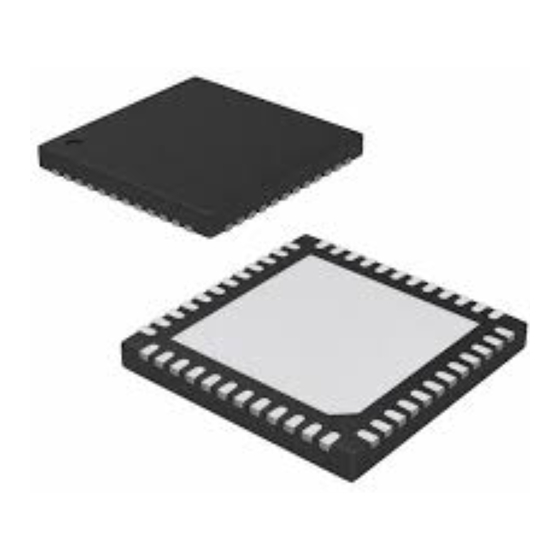
[AK4458] 11. Package ■ Outline Dimensions ■ Material & Lead finish Package molding compound: Epoxy Lead frame material: Lead frame surface treatment: Solder (Pb free) plate 014011794-E-01 2015/08 - 82 -... -
Page 83: Marking
[AK4458] ■ Marking AK4458VN XXXXXXX 1) Pin #1 indication 2) AKM Logo 3) Date Code: XXXXXXX(7 digits) 4) Product Code: AK4458VN 12. Revision History Date (Y/M/D) Revision Reason Page Contents 15/01/23 First Edition 15/08/26 Error 13, 15 Sharp Roll-Off Filter, fs=44.1kHz, DF + SCF, FR: 0 Correction ~ 20kHz, max=0.1dB... -
Page 84: Important Notice
[AK4458] IMPORTANT NOTICE 0. Asahi Kasei Microdevices Corporation (“AKM”) reserves the right to make changes to the information contained in this document without notice. When you consider any use or application of AKM product stipulated in this document (“Product”), please make inquiries the sales office of AKM or authorized distributors as to current status of the Products.
Need help?
Do you have a question about the AK4458 and is the answer not in the manual?
Questions and answers