Advertisement
Quick Links
J
T
A
G
-
H
S
2
J
T
A
G
-
H
S
2
P
r
o
g
r
a
m
m
i
n
g
C
P
r
o
g
r
a
m
m
i
n
g
C
Revision: July 24, 2012
Overview
The Joint Test Action Group (JTAG)-HS2
programming cable is a high-speed
programming solution for Xilinx field-
programmable gate arrays (FPGAs). The cable
is fully compatible will all Xilinx tools and can be
seamlessly driven from iMPACT, Chipscope,
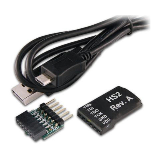
and EDK. The HS2 attaches to target boards
using Digilent's 6-pin, 100-mil spaced
programming header or Xilinx's 2x7, 2mm
connector and the included adaptor.
The PC powers the JTAG-HS2 through the
USB port and will recognize it as a Digilent
programming cable when connected to a PC,
even if the cable is not attached to the target
board. The HS2 has a separate Vdd pin to
supply the JTAG signal buffers. The high speed
24mA three-state buffers allow target boards to
drive the HS2 with signal voltages from 1.8V to
5V and bus speeds of up to 30MBit/sec. (See
figure 1) To function correctly the HS2's Vdd pin
must be tied to the same voltage supply that
drives the JTAG port on the FPGA.
The JTAG bus can be shared with other
devices as systems hold JTAG signals at high-
impedance except when actively driven during
programming. The HS2 comes included with a
standard Type-A to Micro-USB cable that
attaches to the end of the module opposite the
system board connector. The system board
connector should hold the small and light HS2
firmly in place. (See figure 2)
Figure 1
V
IO
VDD (VREF)
GND
USB2
TCK
Port
TDO
TDI
TMS
JTAG-HS2
Doc: 502-249
a
b
l
e
f
o
r
X
i
l
i
n
x
a
b
l
e
f
o
r
X
i
l
i
n
x
: 5V to 1.8V
VIO
GND
TCK
TDO
TDI
TMS
FPGA
F
P
G
A
s
F
P
G
A
s
Small, complete, all-in-one JTAG programming
solution for Xilinx FPGAs
Compatible with all Xilinx tools
Compatible with IEEE 1149.7-2009 Class T0 -
Class T4 (includes 2-Wire JTAG)
Separate Vref drives JTAG/SPI signal voltages;
Vref can be any voltage between 1.8V and 5V.
High-Speed USB2 port that can drive JTAG/SPI
bus at up to 30Mbit/sec
JTAG/SPI frequency settable by user
Uses micro-AB USB2 connector
SPI programming solution (modes 0 and 2 up to
30Mbit/sec, modes 1 and 3 up to 2Mbit/sec)
Fully supported by the Adept SDK, allowing
custom JTAG/SPI applications to be created
1 2 3 4 5 6
Digilent JTAG Header
Single row, 100-mil, 6-pin
1300 Henley Court | Pullman, WA 99163
(509) 334 6306 Voice and Fax
Figure 2
Micro-USB
Xilinx JTAG Header
Dual row, 2-mm, 14-pin
Included
Adaptor
page 1 of 5
Advertisement

Summary of Contents for Digilent JTAG-HS2
- Page 1 Small, complete, all-in-one JTAG programming The PC powers the JTAG-HS2 through the solution for Xilinx FPGAs USB port and will recognize it as a Digilent Compatible with all Xilinx tools programming cable when connected to a PC, Compatible with IEEE 1149.7-2009 Class T0 - even if the cable is not attached to the target board.
- Page 2 Users may utilize the API’s provided by the SDK to create applications that can drive any SPI device supporting those modes. Please see the Adept SDK reference manual for more information. Digilent’s AVR programmer also supports the HS2 and the cable can be used to program any AVR device.
-
Page 3: Design Notes
Class T4 TAP controller using the MScan, OScan0, and OScan1 scan formats. Design Notes The JTAG-HS2 uses high speed three-state buffers to drive the TMS, TDI, and TCK signals. These buffers are capable of sourcing or sinking a maximum of 50 mA of current. The HS2 has 100 ohm resistors between the output of the buffers and the I/O pins to ensure the cable does not exceed the maximum limit. - Page 4 JTAG-HS2 Reference Manual When the JTAG-HS2 first receives power the three-state buffers attached to the TMS, TDI, and TCK signals move into a high-impedance state. They remain in the high-impedance state until an application enables the HS2’s JTAG or SPI port. Once these ports activate, the buffers actively drive the TMS, TDI, and TCK signals until the port is disabled.
-
Page 5: Dc Operating Characteristics
16.6ns 62.5µs to TMS, TDI 15ns TDO Setup time 19ns TDO Hold time Copyright Digilent, Inc. All rights reserved. Other product and company names mentioned may be trademarks of their respective owners. Doc: 502-249 page 5 of 5...
Need help?
Do you have a question about the JTAG-HS2 and is the answer not in the manual?
Questions and answers