
Summary of Contents for LabJack U3
- Page 1 LabJack U3 User’s Guide Revision 1.02 2/6/2007 LabJack Corporation www.labjack.com support@labjack.com...
- Page 2 PC to the real-world. Although LabJacks have various redundant protection mechanisms, it is possible, in the case of improper and/or unreasonable use, to damage the LabJack and even the PC to which it is connected. LabJack Corporation will not be liable for any such damage.
- Page 3 LabJack U3 User’s Guide Revision History V1.00 released December 14 , 2006 V1.01 released January 31 , 2007 Section 2.13 – New section describing changes with hardware revision 1.21. Section 4.2 – Various minor typo corrections. Section 5.2.12 – Various changes to StreamData section.
-
Page 4: Table Of Contents
2.9.2 Timer Operation/Performance Notes ................36 2.10 SCL and SDA (or SCA) ....................36 2.11 DB15..........................36 2.11.1 CB15 Terminal Board ....................37 2.11.2 RB12 Relay Board ....................37 2.12 U3-OEM..........................38 2.13 Hardware Revision Notes....................39 3. Operation ..........................40 3.1 Command/Response......................40 3.2 Stream Mode ........................42 3.2.1 Streaming Digital Inputs, Timers, and Counter0 ............43 4. - Page 5 4.2.17 eAIN()........................58 4.2.18 eDAC() ........................58 4.2.19 eDI() .........................59 4.2.20 eDO() ........................59 4.2.21 eTCConfig() ......................60 4.2.22 eTCValues()......................61 4.3 Example Pseudocode.......................62 4.3.1 Open ...........................62 4.3.2 Configuration.......................62 4.3.3 Analog Inputs ......................63 4.3.4 Analog Outputs ......................65 4.3.5 Digital I/O ........................65 4.3.6 Timers & Counters ......................66 4.3.7 Stream Mode ......................68 4.3.8 Raw Output/Input ......................72 4.3.9 Easy Functions ......................72...
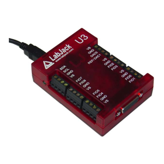
- Page 6 Table Of Figures Figure 1-1. LJControlPanel Main Window..................7 Figure 1-2. LJControlPanel U3 Configure Defaults Window ............8 Figure 1-3. LJControlPanel U3 Test Window................9 Figure 1-4. LJControlPanel Settings Window ................9 Figure 1-5. Self-Upgrade Application ..................10 Figure 2-1. LabJack U3......................12 Table 2-1. Analog Input Pin Locations ..................13 Table 2-2.
-
Page 7: Installation On Windows
CD must be used before installing updates. When the USB cable is connected from the PC to the U3, on a USB port that has not enumerated a U3 before, Windows will bring up the add new hardware wizard. If this is the first time a U3 has been enumerated on any port on the PC, use the “specify location”... -
Page 8: Figure 1-2. Ljcontrolpanel U3 Configure Defaults Window
Figure 1-2. LJControlPanel U3 Configure Defaults Window Figure 1-2 shows the configuration window for U3 defaults. These are the values that will be loaded by the U3 at power-up or reset. The factory defaults, as shown above, are all lines configured as digital input. -
Page 9: Figure 1-3. Ljcontrolpanel U3 Test Window
Figure 1-3. LJControlPanel U3 Test Window Selecting Options=>Settings from the main LJControlPanel menu brings up the window shown in Figure 1-4. This window allows some features to of the LJControlPanel application to be customized. Figure 1-4. LJControlPanel Settings Window... -
Page 10: Self-Upgrade Application (Ljselfupgrade)
Figure 1-5 programs the latest firmware onto the processor. USB is the only interface on the U3, and first found is the only option for self-upgrading the U3, so no changes are needed in the “Connect by:” box. There must only be one U3 connected to the PC when running LJSelfUpgrade. - Page 11 2. If step 1 does not fix the problem unplug the U3 and watch the LED while plugging the U3 back in. Follow the following steps based on the LED's activity. a. If the LED is blinking continuously, connect a jumper between FIO0 and SCL then unplug the U3, wait 5 seconds and plug the U3 back in.
-
Page 12: Hardware Description
(GND), and USB ground is generally the same as the ground of the PC chassis and AC mains. The details of the U3 USB interface are handled by the high level drivers (Windows LabJackUD DLL), so the following information is really only needed when developing low-level drivers. -
Page 13: Status Led
Endpoint 2 OUT is not supported by the firmware, and should never be used. All commands should always be sent on Endpoint 1, and the responses to commands will also always be on Endpoint 1. Endpoint 2 is only used to send stream data from the U3 to the host. 2.2 Status LED There is a green status LED on the LabJack U3. -
Page 14: Ain
2.6 AIN The LabJac k U3 has up to 16 analog inputs available on the flexible I/O lines (FIO0-FIO7 and EIO0-EIO7). Single-ended measurements can be taken of any line compared to ground, or differential measurements can be taken of any line to any other line. -
Page 15: Channel Numbers
LabJack driver. When used, the river will actually pass 30 as the negative channel to the U3, and when the result is returned the driver adds Vref to the value. This results is a full span on the positive channel of about 0 4.88 volts (versus ground), but since the voltage on any analog input cannot exceed 3.6 volts,... -
Page 16: Table 2-6. Nominal Analog Input Voltage Ranges (Dac1 Disabled)
2-4 shows where the var ious calibration values are stored in the Mem area. Generally when communication is initiated with the U3, three calls will be made to the ReadMem func tion to retrieve the first 3 blocks of memory. This information can then be used to convert all a nalog put readings to voltages. -
Page 17: Typical Analog Input Connections
(single-ended) or 2Vreg (differential). .6.3 Typical Analog Input Co nnections A common question is “can this sensor/signal be measured with the U3”. Unless the signal has a voltage (referred to U3 ground) beyond the limits in Appendix A, it can be connected without... - Page 18 Appendix A. When measuring parameters other than voltag or voltages too big or too small for the U3, some sort of sensor or transducer is required to produce the proper voltage signal. Examples are a temperature sensor, amplifier, resistive voltage divider, or perhaps a combination of such things.
- Page 19 LabJack GND. As long as an extreme voltage is not measured, it is generally OK to connect the box ground to LabJack GND, but it is a good idea to put in a 100 Ω series resistor to prevent large currents fro m flowing on the ground.
-
Page 20: Figure 2-2. Non-Inverting Op-Amp Configuration
2.6.3.6 Signal voltages beyond 0-2.44 volts (and resistance measurement) The nominal maximum analog input voltage range for the U3 is 0-2.44 volts. The easiest w ay to handle larger voltage s is often by using the LJTick-Divider, which is a two channel buffered ivider module that plugs into the U3 screw-terminals. -
Page 21: Figure 2-3. Voltage Divider Circuit
For instance, R2 = 9.1 kΩ provides a ivide by 2.1, so a ~0-5 volt input will be scaled to the input range of the U3. The divide by 2 configuration where R1 = R2 = 10 kΩ, presents a 20 kΩ load to the source, meaning that a 5 volt signal will have to be able to source/sink up to 250 µA. -
Page 22: Figure 2-5. Current Measurement With Arbitrary Load Or 2-Wire 4-20 Ma Sensor
If sen sor ground is connected to U3 ground, the sinking type of sensor presents a problem, as at least one sid e of the resistor has a high common mode voltage (equal to the positive sensor supply). If the... -
Page 23: Internal Temperature Sensor
U3 has an internal temperature sensor . Although this sensor measures the temperature side the U3, which is warmer than ambient, it has been calibrated to read actual ambient temperature. For accurate measurements th e temperature of the entire U3 must stabilize relative to the ambient temperature, which ca n take on the order of 1 hour. -
Page 24: Typical Analog Output Connections
2.7.1 Typical Analog Output Connections .7.1.1 High Current Output he DACs on the U3 can output quite a bit of current, but have 50 Ω of source impedance that will cause voltage drop. To avoid this voltage drop, an op-amp can be used to buffer the output, such as the non-inverting configuration shown in Figu re 2-2. -
Page 25: Digital I/O
2.8 Digital I/O The LabJack U3 has up to 20 digital I/O channels. 16 are available from the flexible I/O lines, and 4 dedicated digital I/O (C IO0-CIO3) are available on the DB15 connector. Each digital line can be individually config ured as input, output-high, or output-low. -
Page 26: Typical Digital I/O Connections
U3, then no additional ground connection is used. If the signal is known to not have a common ground with the U3, then the signal ground can simply be connected to U3 GND. If there is uncertainty about the relations etween signal ground and U3 ground (e.g. -
Page 27: Figure 2-9. Driven Signal Connection To Digital Input
5 volts and ground, like the push-pull signal, an open-collector signal provides ground and high-impedance. This type of signal can be thought of as a switch connected to ground. Since the U3 digital inputs have a 100 kΩ internal pull-up resistor, an open-collector signa l can generally be connected directly to the input. -
Page 28: Figure 2-10. Basic Mechanical Switch Connection To Digital Input
0 volts (logic low). Since the mechanical switch does not have any electrical connections, besides to the LabJack, it can safely be connected directly to GND, without using a series resistor or SGND. -
Page 29: Figure 2-12. Relay Connections (Sinking Control, High-Side Load Switching)
when the switch is closed. 1 kΩ limits the maximum current to about 5 mA, but better results might be obtained with smaller resistor values. 2.8.1.4 Output: Controlling Relays All the digital I/O lines have series resistance that restricts the amount of current they can s or source, but solid-state relays (SSRs) can usually be controlled directly by the digital I/O. -
Page 30: Timers/Counters
Another accessory available from LabJack is the LJTick-RelayDriver. This is a two channel odule that plugs into the U3 screw-terminals, and allows two digital lines to each hold off up to 50 volts and sink up to 200 mA. This allows control of virtually any solid-state or mechanical relay. - Page 31 FIO/EIO pin. ote that the DACs (Section 2.x) are derived from PWM signals that are affected by the timer clock frequency. The default timer clock frequency of the U3 is set to 48 MHz, as this resul ts in the minimum DAC output noise.
-
Page 32: Timer Mode Descriptions
732.42 2.861 Note that the clocks above apply to the U3 hardware revision 1.21. With hardware revision 1.20 all clocks are half of those values. The same clock applies to all timers, so all 16-bit PWM channels will have the same frequency and will have their falling edges at the same time. - Page 33 Note that the clocks above apply to the U3 hardware revision 1.21. With hardware revision 1.20 all clocks are half of those values. The same clock applies to all timers, so all 8-bit PWM channels will have the same frequency and will have their falling edges at the same time.
- Page 34 Note that the minimum measurable high/low time is limited by the edge rate limit discussed in Section 2.9.2. When using the LabJackUD driver the value returned is the entire 32-bit value. To determine the high and low time this value should be split into a high and low word. One way to do this is to do a modulus divide by 2 to determine the LSW, and a normal divide by 2 (keep the...
- Page 35 24000000.0 366.211 Note that the clocks above apply to the U3 hardware revision 1.21. With hardware revision 1.20 all clocks are half of those values. The frequency output has a -3 dB frequency of about 10 MHz on the FIO lines. Accordingly, at high frequencies the output waveform will get less square and the amplitude will decrease.
-
Page 36: Timer Operation/Performance Notes
2.9.1.10 System Timer Low/High Read (Modes 10 & 11) The LabJack U3 has a free-running internal 64-bit system timer with a frequency of 4 Mz. Timer modes 10 & 11 return the lower or upper 32-bits of this timer. An FIO line is allocated for these modes like normal, even though they are internal readings and do not require any external connections. -
Page 37: Cb15 Terminal Board
Refer to the specifications in Appendix A. All digital I/O on the U3 have 3 possible states: input, output-high, or output-low. Each bit of I/O can be configured individually. When configured as an input, a bit has a ~100 kΩ pull-up resistor to 3.3 volts. -
Page 38: U3-Oem
2.12 U3-OEM There is an OEM version of the U3 available. It is a board only (no enclosure), and does not have most of the through-hole components installed. The picture below shows how the U3- OEM ships by default. Leaving the through-hole parts off makes the OEM board very flexible. -
Page 39: Hardware Revision Notes
Other new functions are supported, including Watchdog, SPI, Asynch, I2C, and SHT1X. • Typical supply current is 50 mA. Older U3s can be upgraded by LabJack for a small fee. For information about upgrading a rev 1.20 unit, go to labjack.com. -
Page 40: Operation
Feedback function is the primary function d, s it writes and reads virtually all I/O on the U3. The Windows UD driver uses the db ck function under-the-hood to handle most requests besides configuration and stre aming. - Page 41 U3 besides analog inputs (digital I/O, DAC0, timers, and counters). he tables above were measured with U3 hardware version 1.21 which started shipping in late August of 2006. The times could be up to twice as long with hardware version 1.20 or less.
-
Page 42: Stream Mode
Since the data buffer on the U3 is very small it uses a feature called auto-recovery. If the buffe overflows, the U3 will continue streaming but discard data until the bu ffer is emptied, and then data will be stored in the buffer again. -
Page 43: Streaming Digital Inputs, Timers, And Counter0
data is calculated by collecting 128 samples and evaluating the standard deviation (RMS noise). The second ENOB colum n is the noise-free resolution, and is the resolution obtained by all readings. This data is calculated by collecting 128 samples and evaluating the maximum value minus the minimum value (peak-to-peak noise). -
Page 44: Labjackud High-Level Driver
4. LabJackUD High-Level Driver The low-level U3 functions are described in Section 5, but most Windows applications will use the LabJackUD driver instead. The driver requires a PC running Windows 98, ME, 2000, or XP. It is recommende d to install e software before making a USB connection to a LabJack. -
Page 45: Function Flexibility
//eGet (Handle, IOType, Channel, *Value, x1 ngErrorcode = eGet (lngHandle, LJ_ioGET_AI N, 3, &dblValue, 0); the case of the U3, the first example using add/go/get handles both th e DAC command and AIN read in a single low- level call, while in the second example using ePut/eGet two low-level commands are used . -
Page 46: Multi-Threaded Operation
In the sample code, alternate functions (S or SS versions) can generally be substituted as desired, changing the parameter types accordingly. All samples here are written in pseudo-C Functions with an “S” or “SS” appended are provided for programming languages that can’t include the LabJackUD.h file and therefore can’t u se the constants included. - Page 47 left behind. Since each request only uses 44 bytes, and as mentioned the ID's will eventua get recycled, it will not be a huge memory loss. In general, even without this issue, it is strongly commended to not create and destroy a lot of threads. It is terribly slow and inefficient. Use thread pools and other techniques to keep new thread creation to a minimum.
-
Page 48: Function Reference
4.2 Function Reference The LabJack driver file is named LabJackUD.dll, and contains the functions described in this section. Some parameters are common to many functions: • LJ_ERROR – A LabJack specific numeric error code. 0 means no error. (lon g, signed 32-bit integer). -
Page 49: Openlabjack()
Call OpenLabJack() before communicating with a device. This function can be called multiple times, however, once a LabJack is open, it remains open until your application ends (or the DLL is unloaded). If OpenLabJack is called repeatedly with the same parameters, thus requesting the same type of connection to the same LabJack, the driver will simply return the same LJ_HANDLE every time. -
Page 50: Eget() And Eput()
Outputs: • pHandle – A pointer to a handle for a LabJack. 4.2.3 eG ( et ) and ePut() The eGet and ePut functions do AddRequest, Go, and GetResult, in one step. The eGet vers ions are designed for inputs or retrie... -
Page 51: Eaddgoget()
*aRequestErrors, long *GoError, long *aResultErrors) Parameter Descriptio eturns: LabJack errorcodes or 0 for no error. Inputs: • Handle – Handle returned by OpenLabJack(). • NumRequests – This is the number of requests that will be made, and thus the number of results that will be returned. -
Page 52: Go()
IOType, long Channel, double Value, long x1, double UserData) Parameter e scription: Returns: LabJack errorcodes or 0 for no error. Inputs: • Handle – Handle returned by OpenLabJack(). • IOType – The type of request. See Sec tion 4.3. •... -
Page 53: Goone()
GoOne() to actually perform the requests. This f unction causes all requests on one particular LabJack to be performed. After calling GoOne(), ca ll GetResult() o r similar to retrieve any returned data or errors. -
Page 54: Getfirstresult() And Getnextresult()
OR _stdcall GetResult ( LJ_HANDLE Handle, long IOType, long Channel, double *pValue) arameter Description: Returns: LabJack errorcodes or 0 for no error. Inputs: • Handle – Handle returned by OpenLabJack(). • IOType – The type of request. See Section 4.3. •... -
Page 55: Doubletostringaddress()
*pChannel, double *pValue, long *px1, double *pUserData) Parameter Description: Returns: LabJack errorcodes or 0 for no error. Inputs: • Handle – Handle returned by OpenLabJack(). Outputs: • pIOType – A pointer to the IOType of this item in the list. -
Page 56: Stringtoconstant()
Declaration: LJ_ERROR _stdcall StringToDoubleAddress ( const char *pString, double *pNumber, long HexDot) Parameter De scription: Returns: LabJack errorcodes or 0 for no error. Inputs: • pString – A pointer to the string represe ntation. • HexDot – If not equal... -
Page 57: Getdriverversion()
Sends a reset command to the LabJack hardware. Resetting the LabJack does not invalidate the handle, thus the device does not have to be opened again after a reset, but a Go call is likely to fail for a couple seconds after until the LabJack is ready. -
Page 58: Eain()
ChannelP – The positive AIN channel to acquire. • ChannelN – The negative AIN channe l to acquire. For the UE9, this parame is ignored. For single-ended channels on the U3, this parameter should be 31 (see Section 2.6.1). •... -
Page 59: Edi()
Voltage, long Binary, long Reserved1, long Reserved2) Parameter Description: eturns: LabJack errorcodes or 0 for no error. Inputs: • Handle – Handle returned by OpenLabJack(). • Channel – The analog output channel to write to. • Voltage – The voltage to write to the analog output. -
Page 60: Etcconfig()
0, so for instance, Timer1 cannot be enabled without enabling Timer0 also. A nonzero value for an array element specifies to enable that timer. For the U3, this array must always have at least 2 elements. • aEnableCounters – An array where each element specifies whether that counter is enabled. -
Page 61: Etcvalues()
A nonzero value for an array element specifies to update/reset that timer. For the U3, this array must always have at least 2 elements. • aReadCounters – An array where each element specifie s whether to read that counter. -
Page 62: Example Pseudocode
4.3.2 Con g fi uration One of the mo st important operations on the U3 is configuring the flexible I/O as digital or analog. The fo llowing 4 IOTypes are used for that: LJ_ioPUT_... -
Page 63: Configuration
IOType created exactly for this urpose, which does the same thing as the 8 function calls above: ePut (lngHandle, LJ_ioPIN_CONFIGURATION_RESET, 0, 0, 0); here are two IOTypes used to write or read general U3 configuration parameters: LJ_ioPUT_CONFIG LJ_ioGET_CONFIG... - Page 64 LJ_ioGET_AIN //Single-ended. Negative channel is fixed as 31. LJ_ioGET_AIN_DIFF //Specify negative channel in x1. The following are special channels, used with the get/put config IOTypes, to configure parameters that applies to all analog inputs: J_chAIN_RESOLUTION //QuickSample enabled if TRUE. J_chAIN_SETTLING_TIME //LongSettling enabled if TRUE.
-
Page 65: Analog Outputs
//Get the AIN1 voltage. GetNextResult (lngHandle, 0, 0, &dblValue, 0, 0); //Get the AIN1 voltage (special 0-3.6 volt range). etNextResult (lngHandle, 0, 0, &dblValue , 0, 0); 4.3.4 Analog O utputs he IOType to set the voltage on an analog output is: J_ioPUT_DAC The following are IOTypes used to write/read the enable bit for D AC1:... -
Page 66: Timers & Counters
Following is example pseudocode for various digital I/O operations: /Execute the pin_configuration_reset IOType so tha t all //pin assignments are in the factory default conditi //The ePut function is used, which combines the ad go/get. Put (lngHandle, LJ_ioPIN_CONFIGURATION_RESET, 0, 0, 0); //Now, an add/go/get block to execute multiple requests. - Page 67 LJ_tmRISINGEDGES16 //Period input (16-bit, rising edge J_tmFALLINGEDGES16 //Period input (16-bit, falling edges) The following are special channels, used with the get/put config IOTypes, to configure a parameter that applies to all timers/counters: _chNUMBER_TIMERS_ENABLED LJ_chTIMER_CLOCK_BASE J_chTIMER_CLOCK_DIVISOR LJ_chTIMER_COUNTER_PIN_OFFSET ith the clock base special channel above, the following constants are passed in the value parameter to select the frequency: J_tc2MHZ //2 MHz clock base...
-
Page 68: Stream Mode
4.3.7 Stream Mode The highest input data rates are obtained in stream mode, which is support ed with U3 hardware version 1.21 or higher. See Section 3.2 for more information about stream mode. There are five IOTypes used to control streaming:... - Page 69 U3 is acquiring it, and thus there will be data left over in the U3 uffer.
- Page 70 LJ_ioSTART_STREAM, 0, &dblValue, 0); //The actual scan rate is dependent on how the desired scan rate divides into //the LabJack clock. The actual scan rate is returned in the value parameter //from the start stream command. actualScanRate = dblValue;...
- Page 71 This is generally used with a software timed read interval. The number of samples read per loop iteration will vary, but the time per loop iteration will be pretty consistent. Since the LabJack clock could be faster than the PC clock, it is recommended to request more scans than are expected each time so that the application does not get behind.
-
Page 72: Raw Output/Input
LJ_ioR AW_IN When u sing these IOTypes, channel # sp ecifies the desired communication pipe. For the U3, 0 is t he ormal pipe while 1 is the streaming pipe. The number of bytes to write/read is specified in value (1-16384), and x1 is a pointer to a byte array for the data. -
Page 73: Miscellaneous
= %.0f\n",adblCounterValues[0]); 4.3.10 Miscellaneous The U3 has a buzzer that can be used to make noise. The buzzer has a resonant frequency of about 4 kHz where it is the l oudest. The frequency of the signal sent to the buzzer is determined by toggling the signal ev ery n iterations of the main U3 firmware loop. - Page 74 // Channel = 0 buzz for a count, Channel = 1 buzz continuous // Value is the Period // X1 is the toggle count when channel = 0 LJ_i oBUZZER If Channel=1, the buzzer goes continuously unt il commanded again. If Channel=0, the buzzer is toggled the number of time s specified in x1.
-
Page 75: Errorcodes
4.4 Errorcodes All functions return an LJ_ERROR errorcode as listed in the following tables. Errorcode Name Description LJE_UNABLE_TO_READ_CALDATA Warning: Defaults used instead. LJE_DEVICE_NOT_CALIBRATED Warning: Defaults used instead. LJE_NOERROR LJE_INVALID_CHANNEL_NUMBER Channel that does not exist (e.g. DAC2 on a UE9), or data from stream is requested on a channel that is not in the scan list. - Page 76 Errorcode Name Description LJE_TIMER_INVALID_MODE LJE_TIMER_QUADRATURE_AB_ERROR LJE_TIMER_QUAD_PULSE_SEQUENCE LJE_TIMER_BAD_CLOCK_SOURCE LJE_TIMER_STREAM_ACTIVE LJE_TIMER_PWMSTOP_MODULE_ERROR LJE_TIMER_SEQUENCE_ERROR LJE_TIMER_SHARING_ERROR LJE_TIMER_LINE_SEQUENCE_ERROR LJE_EXT_OSC_NOT_STABLE LJE_INVALID_POWER_SETTING LJE_PLL_NOT_LOCKED LJE_INVALID_PIN LJE_IOTYPE_SYNCH_ERROR LJE_INVALID_OFFSET LJE_FEEDBACK_IOTYPE_NOT_VALID LJE_SHT_CRC LJE_SHT_MEASREADY LJE_SHT_ACK LJE_SHT_SERIAL_RESET LJE_SHT_COMMUNICATION LJE_AIN_WHILE_STREAMING AIN not available to command/response functions while the UE9 is streaming. LJE_STREAM_TIMEOUT LJE_STREAM_SCAN_OVERLAP New scan started before the previous scan completed.
-
Page 77: Table 4-3. Group Level Error Codes
1006 LJE_NO_MORE_DATA_AVAILABLE 1007 LJE_LABJACK_NOT_FOUND LabJack not found at the given id or address. 1008 LJE_COMM_FAILURE Unable to send or receive the correct number of bytes. 1009 LJE_CHECKSUM_ERROR... -
Page 78: Low-Level Function Reference
5. Low-Level Function Reference This section describes the low level functions of the U3. These are commands sent over USB directly to the processor on the U3. The majority of Windows users will use the high-level UD driver rather than these low-level functions. - Page 79 -Divide by 2^8 and sum the quotient and remainder. Destination bit: This bit specifies whether the command is destined for the local or remote target. This bit is ignored on the U3. Multi-byte parameters: the following function definitions there are various multi-byte parameters. The least ignificant byte of the parameter will always be found at the lowest byte number.
-
Page 80: Low-Level Functions
5.2 Low-Level Functions 5.2.1 BadChecksum If the processor detects a bad checksum in any command, the following 2-byt e normal response will be sent and nothing further will be done. Response: Byte 0xB8 0xB8... -
Page 81: Configu3
WriteMask, the flash could eventually be damaged. There is a hardware method to restore bytes 9-20 to the factory default value of 0x00. Power p the U3 with a short from FIO2<=>SCL, then remove the jumper and power cycle the device gain. Command:... - Page 82 LocalID: If the WriteMask bit 0 is set, the values passed become the default values, meaning they are written to flash and used at reset. This is a user-configurable ID that can be used to identify a specific LabJack. The return value of this parameter is the current value and the power-up default value.
- Page 83 • SerialNumber: Fixed parameter that is unique for every LabJack. • ProductID: (3) Fixed parameter identifies this LabJack as a U3.
-
Page 84: Configio
5.2.3 ConfigIO Writes and reads the current IO configuration. Command: Byte Checksum8 0xF8 0x03 0x0B Checksum16 (LSB) Checksum16 (MSB) WriteMask Bit 4: Reserved, Pass 0 Bit 3: EIOAnalog Bit 2: FIOAnalog Bit 1: DAC1Enable Bit 0: TimerCounterConfig Reserved TimerCounterConfig Bits 4-7: TimerCounterPinOffset Bit 3: Enable Counter1 Bit 2: Enable Counter0 Bits 0-1: Number of timers enabled... - Page 85 function. Note that Counter0 is not available when using a timer clock base that supports a tim er clock divisor (TimerClockBase = 3-6). • DAC1Enable: Bit 0 enables DAC1. Wh en DAC1 is disabled, it outputs a constant voltage of 1.5 times the internal Vref (~2.44 volts). When DAC1 is enable d, the internal Vref is not available for the analog inputs and Vreg (~3.3 volts) is used as the AIN reference.
-
Page 86: Configtimerclock
5.2.4 ConfigTimerClock Writes and read the timer clock configuration. Comm nd: Byte Checksu 0xF8 0 02 0x0A ecksum16 (LSB) Checksum16 (MSB) Reserved Reserved TimerClockConfig Bit 7: Configure the clock Bits 2-0: TimerClockBase b000: 4 MHz b001: 12 MHz b010: 48 MHz (Default) b011: 1 MHz /Divisor b100: 4 MHz /Divisor b101: 12 MHz /Divisor... -
Page 87: Feedback
5.2.5 Feedback A flexible function that handles all command/response functionality. One or more IOTypes are used to perform a single write/read or multiple writes/reads. Note that the general protocol described in Section 4.1 defines byte 2 of an extended command as the number of data words, which is the number of words in a packet beyond the first 3 (a word is 2 bytes). - Page 88 • ErrorFrame: If Errorcode is not zero, this parameter indicates which IOType caused the error. For ins tance, if the 3 passed IOType caused the error, the ErrorFrame would be equal to 3. Also note that data is only returned for IOTypes before the one that caused the error, so if any IOType causes an error the overall function response will have less bytes than expected.
- Page 89 AIN: IOType=1 AIN, 3 Command Bytes: IOType=1 Bits 4-0: Positive Channel Bit 6: LongSettling Bit 7: QuickSample Negative Channel 2 Res ponse Bytes: AIN LSB AIN MSB This IOType returns a single analog input reading. • Positive Channel: 0-15 for AIN0-AIN15, 30 for temp sensor, or 31 for Vreg. Note that AIN0-AIN7 appear on FIO0-FIO7, and AIN8-AIN15 appear on EIO0-EIO7.
- Page 90 and low, thus providing a simple way to create a pulse. Note that this IOType uses the same internal timer as stream mode, so cannot be used while streaming. • Time: This value (0-255) is multiplied by 32 milliseconds to determine the delay. 5.2.5.4 LED: IOType=9 LED , 2 Command Bytes: IOType=9...
- Page 91 5.2.5.7 BitDirRead: IOType=12 BitDirRead , 2 Command Bytes: IOType=12 Bits 0-4: IO Number 1 Res ponse Byte: Bit 0: Direction This IOType reads the direction of a single bit of digital I/O. This is the digital direction only, and does not provide any information as to whether the line is co nfigured as digital or analog.
- Page 92 .2.5.10 PortStateWrite: IOType=27 PortStateWrite , 7 Command Bytes: IOType=27 WriteMask State 0 Response Bytes: This IOType writes the state of all digital I/O, where 0-7=FIO, 8-15=EIO, and 16-19=CIO. Note that the desired lines must be configured as digital (not analog) and must be configured as output.
- Page 93 digital I/O as output, Direction=d1048575. To configure FIO0-FIO2 as output, EIO0- EIO2 as output, CIO0 as output, and all other I/O as input (b000000010000011100000111), Direction=d67335. 5.2.5.13 DAC#: IOType=34,35 DAC# , 2 Command Bytes: IOType=34,35 Value 0 Response Bytes: s IOType controls a single analog output. •...
- Page 94 • Value: These values are only updated if the UpdateReset bit is 1. The meaning of this parameter varies with the timer mode. 5.2.5.16 Counter#: IOType=54,55 Counter# , 2 Command Bytes: IOType=54,55 Bit 0: Reset 4 Response Bytes: Counter LSB Counter Counter Counter MSB...
-
Page 95: Readmem (Readcal)
5.2.6 ReadMem (ReadCal) Reads 1 block (32 bytes) from the non-volatile user or calibration memory. Command numb 0x2A a ccesses the user memory area which consists of 256 bytes (block numbers 0-7). and number 0x2D accesses the calibration memory are a which consists of 96 bytes lock numbers 0-2). -
Page 96: Writemem (Writecal)
5.2.7 WriteMem (WriteCal) Writes 1 block (32 bytes) to the non-volatile user or calibration memory. Command number 0x28 accesses the user memory area which consists of 256 bytes (block numbers 0-7). Command number 0x2B accesses the calibration memory area which consists of 96 bytes (block numbers 0-2). -
Page 97: Erasemem (Erasecal)
5.2.8 EraseMem (EraseCal) he U3 uses flash memory that must be erased before writing. Command number 0x29 erases e entire user memory area. Command number 0x2C erases the entire calibration memory area. The EraseCal command has two extra constant bytes, to make it more difficult to call the function accidentally. -
Page 98: Reset
5.2.9 Reset Causes a soft or hard reset. A soft reset consists of re-initializing most variables without re- enumeration. A hard reset is a reboot of the processor and does cause re-enumeration. Command: Byte Checksum8 0x99 ResetOptions Bit 1: Hard Reset Bit 0: Soft Reset 0x00 Response:... -
Page 99: Streamconfig
NumChannels: This is the number of channels you will sample per scan (1-25). • SamplesPerPacket: Specifies how many samples will be pulled out of the U3 FIFO buffer and returned per data read packet. For faster stream speeds, 25 samples per... - Page 100 would be desirable for low-latency data retrieval. Note that this parameter is not necessarily the same as the number of channels per scan. Even if only 1 channel is being scanned, SamplesPerPacket will usually be set to 25, so there are usually multiple scans per packet.
-
Page 101: Streamstart
5.2.11 StreamStart Once the stream settings are configured, this function is called to start the stream. Requires hardware version 1.21. Command: Byte 0xA8 0xA8 Response: Byte Checksum8 0xA9 Errorcode 0x00... -
Page 102: Streamdata
100% full. tream mode on the U3 uses a feature called auto-recovery. If the stream buffer fills up, the U3 will go into auto-recovery mode. In this mode, the U3 no longer stores new scans in the buffer, but rather new scans are discarded. -
Page 103: Streamstop
5.2.13 StreamStop Requires U3 hardware version 1.21. Command: Byte 0xB0 0xB0 Response: Byte Checksum8 0xB1 Errorcode 0x00... -
Page 104: Watchdog
(sets bytes 7-10 to 0). ower up the U3 with a short from FIO2<=>SCL, then remove the jumper and power cycle the device again. This also affects the parameters in the ConfigU3 function. - Page 105 Response: Byte Checksum8 0xF8 0x05 0x09 Checksum16 (LSB) Checksum16 (MSB) Errorcode WatchdogOptions TimeoutPeriod DIOConfig Reserved Reserved Reserved Reserved Reserved • WatchdogOptions: Set the appropriate bits to reset the device and/or update the state of 1 digital output. • TimeoutPeriod: The watchdog timer is reset to zero on any incoming USB communication.
-
Page 106: Spi
5.3.15 SPI Requires U3 hardware version 1.21. Sends and receives serial data using SPI synchronous communication. Command: Byte Checksum8 0xF8 4 + NumSPIWords 0x3A Checksum16 (LSB) Checksum16 (MSB) SPIOptions Bit 7: AutoCS Bit 6: DisableDirConfig Bits 1-0: SPIMode (0=A, 1=B, 2=C, 3=D) - Page 107 passing a value of 0 corresponds to a factor of 256, and thus a maximum frequency of about 125 kHz. • CS/CLK/MISO/MOSI -PinNum: Assigns which digital I/O line is used for each SPI line. Value passed is 0-19 corresponding to the normal digital I/O numbers as specified in Section 2.8.
-
Page 108: Asynchconfig
5.3.16 AsynchConfig Requires U3 hardware version 1.21. Configures the U3 UART for asynchronous communication. The UART uses SDA for TX (transmit) and SCL for RX (receive). Communication is in the common 8/n/1 format. Similar to RS232, except that the logic is normal CMOS/TTL. -
Page 109: Asynchtx
5.3.17 AsynchTX Requires U3 h ardware version 1.21. Sends bytes to the U3 UART which will be sent asynchronously on the SDA terminal. Command: Byte Checksum8 0xF8 1 + NumAsynchWords 0x15 Checksum16 (LSB) Checksum16 (MSB) 0x00 NumAsynchBytesToSend AsynchByte0 … …... -
Page 110: Asynchrx
5.3.18 AsynchRX Requir es U3 hardware version 1.21. Reads the oldest 32 bytes from the U3 UART RX buffer (received on SCL termin al). The buffer holds 256 bytes. Comm and: Byte Checksum8 0xF8 0x01 0x16 Checksum16 (LSB) Checksum16 (MSB) -
Page 111: I2C
5.3.19 I2C Requires U3 hardware version 1.21. Sends and receives serial data using I2C sy nchronous communication. Command: Byte Checksum8 0xF8 4+NumI2CWordsSend 0x3B Checksum16 (LSB) Checksum16 (MSB) I2COptions Bit 1: ResetAtStart Bit 0: Reserved SpeedAdjust SDAPinNum SCLPinNum Address Reserved NumI2CBytesToSend... - Page 112 • NumI2CBytesToSend: Specifies how many I2C bytes will be sent (0-242). • NumI2CBytesTo Receive: Specifies how many I2C bytes will be read (0-244). • I2Cbyte#: In the command, these are the bytes to send. In the response, thes e are the bytes read.
-
Page 113: Sht1X
5.3.20 SHT1X Requires U3 hardware version 1.21. Reads temperature and humidity from a Sensirion SHT1X sensor (which is used by the EI-1050). For more informat ion, see the EI-1050 datasheet from labjack.com, and the SHT1X datasheet from sensirion.com. Command: Byte... -
Page 114: Errorcodes
5.3 Errorcodes Following is a list of the low-level function errorcodes. Code SCRATCH_WRT_FAIL SCRATCH_ERASE_FAIL DATA_BUFFER_OVERFLOW ADC0_BUFFER_OVERFLOW FUNCTION_INVALID SWDT_TIME_INVALID XBR_CONFIG_ERROR FLASH_WRITE_FAIL FLASH_ERASE_FAIL FLASH_JMP_FAIL FLASH_PSP_TIMEOUT FLASH_ABORT_RECEIVED FLASH_PAGE_MISMATCH FLASH_BLOCK_MISMATCH FLASH_PAGE_NOT_IN_CODE_AREA MEM_ILLEGAL_ADDRESS FLASH_LOCKED INVALID_BLOCK FLASH_ILLEGAL_PAGE FLASH_TOO_MANY_BYTES FLASH_INVALID_STRING_NUM SHT1x_COMM_TIME_OUT SHT1x_NO_ACK SHT1x_CRC_FAILED SHT1X_TOO_MANY_W_BYTES SHT1X_TOO_MANY_R_BYTES SHT1X_INVALID_MODE SHT1X_INVALID_LINE STREAM_IS_ACTIVE STREAM_TABLE_INVALID STREAM_CONFIG_INVALID... - Page 115 Errorc odes (Continued): Code TIMER_INVALID_MODE TIMER_QUADRATURE_AB_ERROR TIMER_QUAD_PULSE_SEQUENCE TIMER_BAD_CLOCK_SOURCE TIMER_STREAM_ACTIVE TIMER_PWMSTOP_MODULE_ERROR TIMER_SEQUENCE_ERROR TIME R_LINE_SEQUENCE_ERROR TIMER_SHARING_ERROR EXT_OSC_NOT_STABLE INVALID_POWER_SETTING PLL_NOT_LOCKED INVALID_PIN PIN_CONFIGURED_FOR_ANALOG PIN_CONFIGURED_FOR_DIGITAL IOTYPE_SYNCH_ERROR INVALID_OFFSET IOTYPE_NOT_VALID...
-
Page 116: Specifications
(3) These specifications are related to the power provided by the host/hub. Self- and bus-powered describes the host/hub, not the U3. Self-powered would apply to USB hubs with a power supply, all known desktop computer USB hosts, and some notebook computer USB hosts. An example of bus-powered would be a hub with no power supply, or many PDA ports. The... - Page 117 (4) The analog inputs essentially connect directly to a SAR ADC on the U3, presenting a capacitive load to the signal source. The key specification is the maximum source impedance. As long as the source impedance is not over this value, there will be no additional errors do to impedance problems.
- Page 118 (3) Maximum voltage to avoid damage to the device. Protection works whether the device is powered or not, but continuous voltages over 5.8 volts or less than -0.3 volts are not recommened when the U3 is unpowered, as the voltage will attempt to supply operating power to the U3 possibly causing poor start-up behavior.
-
Page 119: Enclosure & Pcb Drawings
B. Enclosure & PCB Drawings The square holes shown below are for a DIN rail mounting adapter: Tyco pa rt #TKAD. Units are inches.
Need help?
Do you have a question about the U3 and is the answer not in the manual?
Questions and answers