Table of Contents
Advertisement
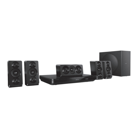
Home Theater BD Player
Service
Service Manual
©Copyright 2013 Philips Consumer Electronics B.V. Eindhoven, The Netherlands
All rights reserved. No part of this publication may be reproduced, stored in aretrieval system or
transmitted, in any form or by any means, electronic, mechanical, photocopying, or otherwise
without the prior permission of Philips.
Published by Arya & Stephen - 1306 Printed in The Netherlands Subject to modification
Version 1.1
Downloaded from
www.Manualslib.com
TABLE OF CONTENTS
. Location of PCB Boards,Version Variation and Repair Scenario Matrix.....1-2
. Technical Specifications.........................................................1-3
. Safety Instruction, Warning & Notes........................................1-4
. DFU Instruction..............................................................................2-1
. Mechanical and Dismantling Instructions....................................3-1
. Software Upgrades .......................................................................
. Trouble Shooting Chart......................................................
. Wiring Diagram..................................................................6-1
. Electrical Diagrams and Print-layouts......................................7-1
. Votages and Waveforms for Connection Pins...........................8-1
. Pin Description & Block Diagrams of ICs..................................9-1
. Set Mechanical Exploded view & Part list...............................10-1
. Revision List.................................................................................11-1
manuals search engine
HTB3510/12/98/X78/40/94/51/93/55
Page
4-1
.
5-1
.
LASER PRODUCT
PHILIPS
CLASS 1
GB
3141 785 39181
Advertisement
Table of Contents

Subscribe to Our Youtube Channel
Related Manuals for Philips HTB3510/12


Summary of Contents for Philips HTB3510/12
-
Page 1: Table Of Contents
. Set Mechanical Exploded view & Part list.…………………..….…10-1 . Revision List.................11-1 CLASS 1 ©Copyright 2013 Philips Consumer Electronics B.V. Eindhoven, The Netherlands All rights reserved. No part of this publication may be reproduced, stored in aretrieval system or LASER PRODUCT transmitted, in any form or by any means, electronic, mechanical, photocopying, or otherwise without the prior permission of Philips. - Page 2 PCB Board Locations VERSION VARIATIONS Type / Versions HTB3510 Service Policy X/78 Board in used MAIN BOARD M+C M+C M+C M+C M+C M+C M+C M+C POWER BOARD M+C M+C M+C M+C M+C M+C M+C M+C AMPLIFIER BOARD M+C M+C M+C M+C M+C M+C M+C M+C FRONT CONTROL BOARD M+C M+C M+C M+C M+C M+C M+C M+C LOADER...
-
Page 3: Specifications
Product File formats specifications Audio: .aac, .mka, .mp3, .wma, .wav, .mp4, .m4a, China) Video: Note .avi, .divx, .mp4, .m4v, .mkv, .asf, .wmv, notice. .rmvb, .rm, .rv (Available only in Asia Picture: .jpg, .jpeg, .jpe, .gif, .png Region codes Audio formats The type plate on the back or bottom of the home theater shows which regions it supports. -
Page 4: Video Formats
AAC, Upto 192 kbps Audio codec Video codec Bit rate PCM, Dolby DivX 3.11, AAC, Upto 192 Digital, MP3, DivX 4.x, DivX 5.x, Mbps kbps DivX 6.x Cook 96469 bps FLAC FLAC Upto 24 Audio codec Video codec Bit rate Dolby Digital, MPEG 1, 40 Mbps... - Page 5 Input sensitivity: AUX: 2 V Audio codec Video codec Bit rate AUDIO IN: 1 V Dolby Digital, MPEG 4 ASP 38.4 Mbps MP3, WMA, Video H.264/AVC 25 Mbps Signal system: PAL / NTSC HDMI output: 480i/576i, 480p/576p, 720p, HiP@4.2 1080i, 1080p, 1080p24 WMV9 45 Mbps Audio...
-
Page 6: Remote Control Batteries
Russia/India: 220-240 V~, 50 Hz Cable length (rear): 10.25 m Power consumption: 160 W Remote control batteries Dimensions (WxHxD): 435 x 58 x 280 2 x AAA-R03-1.5 V Weight: 2.66 kg Laser Subwoofer Laser Type (Diode): InGaN/AIGaN (BD), Output power: 166 W RMS (30% THD) AIGaInP (DVD/CD) Impedance: 4 ohm Wave length: 405 +7 nm/-7 nm (BD),... -
Page 7: Safety Instruction, Warning & Notes
Safety instruction, Warning & Notes Safety instruction 1. General safety 2.Laser safety Safety regulations require that during a repair: This unit employs a laser. Only qualified service personnel . Connect the unit to the mains via an isolation transformer. may remove the cover, or attempt to service this device . - Page 8 Warning 1.General 2. Laser . All ICs and many other semiconductors are susceptible to . The use of optical instruments with this product, will electrostatic discharges (ESD). Careless handing during increase eye hazard. repair can reduce life drastically. Make sure that, during .
- Page 9 Solder Joint Downloaded from www.Manualslib.com manuals search engine...
- Page 10 - lead free BGA-ICs will be delivered in so-called respected by the workshop during a repair: ‘dry-packaging’ (sealed pack including a silica gel Use only lead-free solder alloy Philips SAC305 with pack) to protect the IC against moisture. After order code 0622 149 00106. If lead-free solder-paste is...
- Page 11 EN Before using your product, read all accompanying safety information DA Læs alle medfølgende sikkerhedsoplysninger, inden du tager produktet i brug PT Antes de utilizar o produto, leia todas as informações de begleitenden Sicherheitsinformationen segurança que o acompanham ES Antes de usar el producto, lea toda la información de seguridad adjunta disertakan okuyun...
- Page 12 EN Connect the home theater IT Collegamento del sistema Home Theater NL Sluit de home cinema aan DA Tilslut hjemmebiografen NO Koble til hjemmekinoanlegget DE Anschließen des Home PL Po Entertainment-Systems PT Efectuar as ligações ao sistema de cinema em casa RO Co ES Conecta el sistema de cine en casa SK Pr...
- Page 13 seguito szerint HDMI ARC HDMI HDMI OUT (ARC) TO TV HDMI IN (ARC) HDMI + OPTICAL OPTICAL HDMI DIGITAL IN HDMI OUT (ARC) TO TV OPTICAL HDMI IN OPTICAL OUT Downloaded from www.Manualslib.com manuals search engine...
- Page 14 HDMI + COAXIAL COAXIAL HDMI HDMI OUT (ARC) TO TV DIGITAL IN COAXIAL HDMI IN COAXIAL OUT HDMI + AUDIO L/R AUDIO L/R HDMI HDMI OUT (ARC) TO TV HDMI IN AUDIO OUT AUDIO IN Downloaded from www.Manualslib.com manuals search engine...
- Page 15 EN Switch on the home theater NL Schakel de home cinema in CS Za NO Sl DA Tænd for hjemmebiografen DE Einschalten des Home PT Ligar o sistema de cinema em casa Entertainment-Systems RO Po SK Za ES Enciende el sistema de cine en casa rran kytkeminen kotiteatteriin FR Me HU A...
- Page 16 EN Co ltooi de eerste installatie CS Do PL Pi ldfør den indledende opsætning DE Abschließen der Ersteinrichtung PT Ex RO Re SK Do SV Sl Ensiasennuksen suorittaminen loppuun FR Ef HU Az IT Co HDMI č Български čΙ ă Č...
- Page 17 EN Use your home theater IT Utilizzo del sistema Home Theater CS Po NL Uw home cinema bedienen DA Brug af din hjemmebiograf NO Bruke hjemmekinoanlegget PL Korzystanie z zestawu kina domowego rwenden des Home Entertainment-Systems PT Utilizar o sistema de cinema em casa RO Ut ES Uso del sistema de cine en casa SK Po...
- Page 18 3.5MM STEREO AUDIO IN Downloaded from www.Manualslib.com manuals search engine...
- Page 19 Downloaded from www.Manualslib.com manuals search engine...
-
Page 20: Mechanical And Dismantling Instructions
Mechanical and Dismantling Instructions Dismantling Instruction Detailed information please refer to the model set. The following guidelines show how to dismantle the player. Step 1:Open the top cover.Remove 4 screws on the back panel,dismantle the left and right baffles,then open the top cover.(Figur 1) Figue 1 Downloaded from www.Manualslib.com... - Page 21 Mechanical and Dismantling Instructions Dismantling Instruction Detailed information please refer to the model set. The following guidelines show how to dismantle the player. Step 2:Dismantle the loader.Open the tray,diamantle the CD door,disconnect connectors(J11,XP7), remove 2 screws beside the loader,then pull up the loader.(Figure 2) Step 3:Dismantle the main board.Disconnect connectors(XP6,XP9,XP4,XP13,XP15),remove 2 screws on the main board and 3 screws on the back panel.then pull up the main board.(Figure 2) Step 4:Dismantle the amplifier board.Disconnect connectors(XP3,XP58),remove 2 screws on the...
-
Page 22: Software Upgrades
4‐1 Software upgrade 1.Build a folder name as UPG under root menu of USB device. 3.Copy the HTB3570.bin file(upgrade file) to the root menu of USB device. 4.Connect the USB device to HTS , 5.Power on DUT,enter into HOME UI. 6.Enter into Setup menu select Advance >>Software upgrade>>USB. If the upgrade SW was found ,it will prompt start upgrade SW,pls press ok select Start. 7.Don’t power off DUT .DUT will restart after SW upgrade completed. Caution: The set must not be power off during upgrading, Otherwise the Main board will be damaged entirely. Downloaded from www.Manualslib.com manuals search engine... -
Page 23: Trouble Shooting Chart
Trouble shooting Chart LED No display on Front Control Board LED No display on Front Control Board Check every supply voltage on Main Board whether normal or not. Refer to CON501 on Power Board (XP4 PIN4&PIN5:+12V) Check voltage +5V on main Board at XP9 Check whether U11 and U10 work PIN16: +5V good or not? And fix it or replace the... - Page 24 Trouble shooting Chart keys do not work keys do not work Check voltage +5V on Front Board U135 Fix the connection XP15 to XP9 on Main PIN7&PIN21 Board Check Front Control Board signals at XP15 Pin5 VSTB, Pin6 VSCLK, Pin7 VSDA Replace U8 on Main Board, or replace Main Board Replace U301 on Front Board...
- Page 25 Trouble shooting Chart Remote control does not work Remote control does not work Check battery of remote control whether exhausted or not. Replace the battery for remote control Check power supply of IR601 on Front Check the +3.3V net on Front Control Board whether normal or not Control Board to Main Board XP9 XP15 Pin10 :+3.3V...
- Page 26 Trouble shooting Chart No audio output No audio output Check XP4 Pin1 5V on Main Board Check voltage +34V for whether normal or whether normal or not not at on Amplifier Board Refer to CON502 on Power Board Check the 24Pin FFC connection XP13 on Main Board and XP1 on Amplifier Board whether right or not between Main Board and Amplifier Board...
- Page 27 Trouble shooting Chart No video output No video output Check L452, R616 whether right on Main Add L452, R616 Board Check the video signal whether right at U1: PIN B18 or R615 Replace Main IC or Main Board Downloaded from www.Manualslib.com manuals search engine...
- Page 28 Trouble shooting Chart Can’t read disc or can’t open the disk door Can’t read disc or can’t open the disk door Check loader work normally or not Check XP7 on Main Board Check 45Pin, 8Pin, 4Pin cable from Fix 45Pin, 8Pin, 4Pin cable Main Board to Loader connect right or Replace Loader 、...
- Page 29 Trouble shooting Chart Tuner FM does not work Tuner FM does not work Check voltage at Q28 C electrode Check whether U11 and U10 work (+5V) on Main Board whether normal good or not? And fix it or replace the or not main board.
- Page 30 Trouble shooting Chart AUX in does not work AUX in does not work Check voltage at U18 PIN16 (6V),check 12V on Main Board whether normal or not Refer to Power Board CON501 Check Main Board U18 Pin4, Pin11 signal input whether right or not Check AUX IN connector Check 74HC4052...
- Page 31 Trouble shooting Chart MP3 Link does not work MP3 Link does not work Check signal XP15 PIN16:MP3_R PIN14:MP3_L ON front board whether normal Refer to Main Board XP9 or not Check Main Board U18 74HC4052 PIN2, Check Main Board C361, C352, R352, PIN15 L/R signal input right or not R458 Check voltage at U18 PIN16 (6V), check...
- Page 32 5-10 Trouble shooting Chart COAX in does not work COAX in does not work Check voltage at U27 PIN6/PIN23:3.3V on Main Board whether normal or not Check power supply circuit. Check Main Board U27 CS8416 PIN3 input Check Main Board C360, L11 signal whether normal or not Check U27 CS8416 whether broken.
- Page 33 5-11 Trouble shooting Chart Karaoke in does not work Karaoke in does not work Check signal XP15 PIN18:MIC_in signal from front board normal or not Refer to Main Board XP9 Check Main Board U18 74HC4052 PIN5, Check the cable between XP9 and XP15 PIN14 L/R signal input right or not Check U18 74HC4052 whether broken Check Main Board U26...
- Page 34 5-12 Trouble shooting Chart Network in does not work Network does not work Check P3 Pin1, Pin2, Pin3, Pin6 from netting twine normal or not Check netting twine link normal or Replace P3 Downloaded from www.Manualslib.com manuals search engine...
- Page 35 Block Diagram for HTB3510: TUNER SPK L 4052*2 L/R PWM ARC(OPTI) BD BOARD I/O*3 SDIN AK5358 ASCLK AUDIO ALRCLK MT8560 PROCESSOR SPK R TI5538 TAS5352*2 CS8416 I2S_SDATA0 I2S_LRCK I2S_SDATA1 I2S_SDATA2 I2S_SCLK SUB PWM I2S_MCLK RESET SPK SUB I2C_SCL I2C_SDA AMP_MUTE MOTOR RESET DRIVER...
- Page 36 Front Control Board Circuit Diagram: +12V MIC_Detect VFD_STB VFD_CLK VFD_DATA KEY_POW 3.3V_STBY IR_IN OPEN/CLOSE R694 R694 R703 R703 R704 R704 R705 R705 MP3_L 4.7K 4.7K 4.7K 4.7K 4.7K 4.7K MP3_R C778 C778 C779 C779 U301 U301 47pF/50V/NP0 47pF/50V/NP0 47pF/50V/NP0 47pF/50V/NP0 DRIVER_LED_ET6202 DRIVER_LED_ET6202 GRID[1:7]...
- Page 37 Power Board Circuit Diagram: CY505 CY505 470pF/250VAC 470pF/250VAC 01U0PWOPP-PW101 C507 2200pF/1KV C507 2200pF/1KV R527 R527 JP509 JP509 T502 T502 NC/Jumper NC/Jumper PQ3230 PQ3230 C506 C506 10/1W 10/1W R515 R515 +34V_1 +34V 0.0022uF(222)400V 0.0022uF(222)400V ZD508 ZD508 R516 R516 R517 R517 R518 R518 D514 SF20A300HPI/20A/300V D514 SF20A300HPI/20A/300V...
- Page 38 Amplifier Board Circuit Diagram:DSP WL_IRQ ADD FB8 AND +12V-FAN +3.3V WL_RST WL_IRQ NET FOR FAN WL_SDA WL_SCL +12V-FAN 24PIN/0.5mm 24PIN/0.5mm 70/1A 70/1A TP24 TP24 NC/4.7K NC/4.7K 4.7K 4.7K 4.7K 4.7K 4.7K 4.7K 4.7K 4.7K 4.7K 4.7K 4.7K 4.7K 4.7K 4.7K LRCLKO SCLKO MCU_CON...
- Page 39 Amplifier Board Circuit Diagram:SL+SW R135 R135 +12V WIRE WIDE=3MM WIRE WIDE=1MM R136 R136 C135 C135 C133 C133 C134 C134 0.1uF/50V/X7R 0.1uF/50V/X7R 0.1uF/50V/X7R 0.1uF/50V/X7R 0.1uF/50V/X7R 0.1uF/50V/X7R TP33 TP33 WIRE WIDE=3MM +34V C136 C136 CEN+ 0.1uF/50V/X7R 0.1uF/50V/X7R GVDD_B GVDD_A 0.033uF/50V/X7R 0.033uF/50V/X7R R137 R137 C137 C137...
- Page 40 Amplifier Board Circuit Diagram:SL+SW +12V LAYOUT NOTE 0.1uF/50V/X7R 0.1uF/50V/X7R 0.1uF/50V/X7R 0.1uF/50V/X7R 0.1uF/50V/X7R 0.1uF/50V/X7R PLACE ON TP25 TP25 COMPONENT SIDE +34V 0.1uF/50V/X7R 0.1uF/50V/X7R WIRE WIDE=5MM GVDD_B GVDD_A 0.033uF/50V/X7R 0.033uF/50V/X7R {4,5} BST_A NOTE ALL CHANEL POWER SUPPLY NET \SPEAKER OUT NET AND ITS WIRE WIDE=3.5MM 1000pF/50V/X7R 1000pF/50V/X7R 0.22uF/50V/X7R...
- Page 41 Front Control Board Print-layout(top side): Downloaded from www.Manualslib.com manuals search engine...
- Page 42 Power Board Print-layout(top side): Downloaded from www.Manualslib.com manuals search engine...
- Page 43 Amplifier Board Print-layout(bottom side): Downloaded from www.Manualslib.com manuals search engine...
- Page 44 Amplifier Board Print-layout(top side): Downloaded from www.Manualslib.com manuals search engine...
- Page 45 Voltages for per connect pin XP4‐‐From Main Board Connect to Power Board XP13‐‐From Main Board Connect to Amp Board Pin No Pin Assin Remarks Pin No Pin Assin Remarks VCC_D 4.75‐5.25V DATA0 LRCKL DATA1 +12V 11.4‐12.6V DATA2 +12V 11.4‐12.6V BCLK XP9‐‐From Main Board Connect to Front Board MCLK Pin No Pin Assin Remarks MIC_in AMP_SCL AGND AMP_SDA MP3_R AGND AMP_MUTE MP3_L AMP_RST 3.3V 3.2‐3.4V OPEN/CLOSE 3.3V +12V_D 11.4‐12.6V IR_OUT 3.3V...
- Page 46 Waveforms for measure point 图1.XP11.1 DATA0 图2.XP11.2 LRCKL 图3.XP11.3 DATA1 图4.XP11.4 DATA2 图5.XP11.5 BCLK 图6.XP11.7 MCLK Downloaded from www.Manualslib.com manuals search engine...
- Page 47 Waveforms for measure point 图7.XP11.9 AMP_SCL 图8.XP11.10 AMP_SDA 图9.XP11.12 AMP_MUTE 图10.XP11.13 AMP_RST 图11.XP11.20 图12.XP11.23 PDWN Downloaded from www.Manualslib.com manuals search engine...
- Page 48 FUNCTIONAL BLOCK DIAGRAM FOR MAIN IC MT8560 NAND DDR3 256/384MB Audio 7.1 CH 2 CH MT8560 S/PDIF Motor Driver HDMI HD+SD Decode Component 810MHz ARM11 Ethernet CVBS 400MHz AudioDSPx3 HDMI 1.4 Ethernet Downloaded from www.Manualslib.com manuals search engine...
-
Page 49: Pin Assignment
PIN ASSIGNMENT Downloaded from www.Manualslib.com manuals search engine... - Page 50 PIN DESCRIPTION Symbol Type Description Digital power/ground DVCC12_K Power 1.2 V digital power Downloaded from www.Manualslib.com manuals search engine...
- Page 51 Symbol Type Description DGND12_K Ground Digital ground AA19 AB13 AC18 Downloaded from www.Manualslib.com manuals search engine...
- Page 52 Symbol Type Description DVCC33_IO Power 3.3 V digital IO power DVCC33_IO_S Power 3.3 V digital IO power for Stand-By Module DDRVCCIO Power 1.5 V digital IO power XTAL/PLL AVDD33_MEM AA21 Power 3.3 V Analog Power for MEMPLL AVSS33_MEM AB19 Ground Analog Ground for MEMPLL AA22 TN_MEMPLL...
- Page 53 Symbol Type Description Audio PWM DAC interface AVDD33_DAC Power 3.3V Analog Power AVSS33_DAC Ground Analog Ground Multiple function: (1) Audio output bit clock (2) Audio PWM output (3) GPIO Multiple function: (1) Audio output master clock (2) Audio PWM output (3) GPIO Audio interface Multiple function:...
- Page 54 Symbol Type Description Multiple function: (1) Audio output serial data 1 (2) Audio output master clock (3) Micophone input master clock (4) Video out DE signal AOSDATA1 (5) External Interrupt 1 (6) 3th RS232 TX (7) Slave I2C clock (8) PWM control signal output (9) Ethernet Activity LED (10) GPIO Multiple function:...
- Page 55 Symbol Type Description Multiple function: SPDIF (1) SPDIF digital audio output (2) GPIO Analog Video Out Interface AVDD33_VDA Power 3.3V Analog Power AVDD33_VDA Power 3.3V Analog Power AVSS33_VDAC Ground Analog Ground AVSS33_VDAC Ground Analog Ground VDACB_OUT Analog DAC output VDACG_OUT Analog DAC output VDACR_OUT...
- Page 56 Symbol Type Description Multiple function: (1) Video out 16-bit 422 mode: C0 (2) External Interrupt 4 (3) 3th RS232 RX VOUTD0 (4) Ethernet Link LED (5) NAND Flash Data input/output bit 4 (6) Secure Disk interface data bit 1 (7) GPIO Multiple function: (1) Video out 16-bit 422 mode: C1 (2) Slave I2C clock...
- Page 57 9-10 Symbol Type Description Multiple function: (1) Video out 16-bit 422 mode: Y0 (2) Microphone input master clcok (3) 2nd RS232 TX VOUTD8 (4) Slave I2C clock (5) PWM control signal output (6) Ethernet Activity LED (7) NAND Flash Data input/output bit 1 (8) GPIO Multiple function: (1) Video out 16-bit 422 mode: Y1...
- Page 58 9-11 Symbol Type Description Multiple function: (1) Video out 16-bit 422 mode: Y5 (2) SPDIF input bit clock (3) 2nd RS232 RX VOUTD13 I/O, 5V (4) Slave I2C data (5) External Interrupt 1 (6) Ethernet Duplex LED (7) NAND Flash command latch enable (8) GPIO Multiple function: (1) Video out 16-bit 422 mode: Y6...
- Page 59 9-12 Symbol Type Description CLK_P Analog HDMI TX clock differential pair (P) NAND Flash Interface Multiple function NFALE (1) NAND Flash address latch enable (2) GPO Multiple function NFCEN (1) NAND Flash chip enable (2) GPO Multiple function (1) NAND Flash 2 chip enable (2) 2nd RS232 TX (3) External Interrupt 2...
- Page 60 9-13 Symbol Type Description Multiple function NFD7 (1) NAND Flash Data input/output bit7 (2) GPIO Multiple function NFRBN (1) NAND Flash ready/busy (2) GPIO Multiple function (1) NAND Flash 2 ready/busy (2) 2nd RS232 RX (3) External Interrupt 1 NFRBN2 (4) 3th RS232 RX (5) Slave I2C data (6) PWM control signal output...
- Page 61 9-14 Symbol Type Description AE24 RBA1 Memory bank address bit 1 AD24 RBA2 Memory bank address bit 2 AC22 RCAS_ Memory column address strobe AE23 RCKE Memory clock enable RCLK0 Memory clock 0 positive RCLK0_ Memory clock 0 negative RCS_ Memory chip select RDQ0 Memory data bit 0...
- Page 62 9-15 Symbol Type Description RRAS_ Memory row address strobe RVREF0 Memory VREF AE25 RWE_ Memory write enable AC25 RRESET Memory reset DRAM Channel B AC10 RA0_B Memory address bit 0 RA1_B Memory address bit 1 RA2_B Memory address bit 2 AB10 RA3_B Memory address bit 3...
- Page 63 9-16 Symbol Type Description AE13 RDQ3_B Memory data bit 3 AD21 RDQ4_B Memory data bit 4 AC21 RDQ5_B Memory data bit 5 AD20 RDQ6_B Memory data bit 6 AC20 RDQ7_B Memory data bit 7 AC15 RDQ8_B Memory data bit 8 AC16 RDQ9_B Memory data bit 9...
- Page 64 9-17 Symbol Type Description Multiple function (1) Serial interface control line GPIO0 I/O, 5V (2) Slave I2C clock (3) External Interrupt 3 (4) GPIO Multiple function (1) Serial interface data line GPIO1 I/O, 5V (2) Slave I2C data (3) External Interrupt 3 (4) GPIO Multiple function (1) Video output DE signal...
- Page 65 9-18 Symbol Type Description Multiple function (1) Microphone input bit clock (2) 3th RS232 TX (3) External Interrupt 2 GPIO6 I/O, 5V (4) Slvae I2C clock (5) PWM control signal output (6) Ethernet Speed LED (7) GPIO Multiple function (1) Microphone input master clock (2) 3th RS232 RX (3) External Interrupt 4 GPIO7...
- Page 66 9-19 Symbol Type Description Reserved for debug-only Uart pins UATXD I/O, 5V (1) 1 RS232 TX (2) T8032 RS232 TX Multiple function (1) VFD clock VCLK I/O, 5V (2) GPIO (3) Slave I2C data (4) Serial interface data line Multiple function (1) VFD data VDATA I/O, 5V...
- Page 67 9-20 Symbol Type Description AVDD33_COM Power PLL/BG 3.3V analog power AVSS33_LD Ground Line driver analog ground AVSS33_PLL Ground PLL/BG analog ground AVDD12_REC Power ADC analog power AVSS12_REC Ground ADC analog ground TXVP_0 Analog Ethernet TD+ TXVP_1 Analog Ethernet RD+ TXVN_0 Analog Ethernet TD- REXT...
- Page 68 9-21 Symbol Type Description 3.3V LVTTL High frequency modulation mode selection signal output, or I/O, LDD serial interface command enable. The pin is spike-free at 5V-tolerance, power-on stage. Slow slew, FECMOD 2, 4, 6, 8mA PDR, 75K pull- down (0V) Analog Disk motor control output.
- Page 69 9-22 Symbol Type Description 3.3V LVTTL LDD serial interface data. The pin is spike-free at power-on I/O, stage. The pin is not allowed to pull-up in circuit layout. 5V-tolerance, Alternate function: FEGIO0 2,4,6,8 mA 1. Internal monitored signal output PDR, 2.
- Page 70 9-23 Symbol Type Description Read gain switch 6. The pin is not allowed to pull-up in circuit layout. Alternate function : Analog FEGIO6 1. SIDM Output 2. LCD serial interface command enable. 3. Internal monitored signal output 4. General IO. 3.3V LVTTL General IO.
- Page 71 9-24 Symbol Type Description 3.3V LVTTL High frequency modulation enable signal output, or LDD serial I/O, interface CLK or I2C SCL. The pin is spike-free at power-on 5V-tolerance, stage. Slow slew, FEOSCEN 2, 4, 6, 8mA PDR, 75K pull-up (3,3V) RFIN Differential Input of AC Coupling RF SUM Signal (Negative) Analog Input...
- Page 72 9-25 Symbol Type Description Analog Output Voltage 3 of Laser Diode Control in APC VWDC3O Output Downloaded from www.Manualslib.com manuals search engine...
- Page 73 10-1 10-1 Exploded View for HTB3510/12/93/94: Downloaded from www.Manualslib.com manuals search engine...
- Page 74 10-2 10-2 Exploded View for HTB3510/98/X78/55/51/40: Downloaded from www.Manualslib.com manuals search engine...
-
Page 75: Revision List
1 1 - 1 Revision List Version 1.0 Initial Release for HTB3510/12: Version 1.1 Initial Release for HTB3510/98/X78/40/51/94/55/93 Downloaded from www.Manualslib.com manuals search engine...
Need help?
Do you have a question about the HTB3510/12 and is the answer not in the manual?
Questions and answers