Table of Contents
Advertisement
Table Of Contents
Service Manual
COVER
1 Note
TOP NEXT
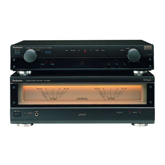
2 Location of Controls
3 To Supply Power Source
AD9907176C2
3.1 Power Supply to Main
Circuit
3.2 Operation Check
4 Operation Checks and
Component
ReplacementProcedures
5 Type Illustration of ICs,
Transistors and Diodes
Control Amplifier
6 Schematic Diagram
6.1 Schematic Diagram
SU-C909U
Notes
6.2 Schematic Diagram
Colour
7 Printed Circuit Board
Diagram
(K)..........Black Type
8 Block Diagram
9 Wiring Connection
Area
Diagram
10 Measurements and
(E)..........Europe and Russia.
Adjustments
10.1 Measurement
instruments and Special tools
10.2 Output Voltage
Adjustment
11 Terminal Function of
ICs
11.1 IC701
(M38503M2404F) : Micro
Computer
12 Replacement Parts List
PV
13 Cabinet Parts Location
PV
14 Packaging
Advertisement
Table of Contents


Need help?
Do you have a question about the SU-A909 and is the answer not in the manual?
Questions and answers
Good morning. I have a Technics SU-Z900 Amp, and I need the power button. Do you have one.? Thank you.