Atari CX 5200 Service Manual
Hide thumbs
Also See for CX 5200:
- Field service manual (187 pages) ,
- Field service manual (180 pages) ,
- Field service manual (170 pages)
Table of Contents
Advertisement
Quick Links
Advertisement
Table of Contents

Related Manuals for Atari CX 5200


Summary of Contents for Atari CX 5200
- Page 2 ATARI ATARI ATARI ATARI ADVANCED VIDEO ENTERTAINMENT SYSTEM ADVANCED VIDEO ENTERTAINMENT SYSTEM ADVANCED VIDEO ENTERTAINMENT SYSTEM ADVANCED VIDEO ENTERTAINMENT SYSTEM MODEL 5200 MODEL 5200 MODEL 5200 MODEL 5200 FIELD SERVICE MANUAL FIELD SERVICE MANUAL FIELD SERVICE MANUAL FIELD SERVICE MANUAL...
- Page 3 Atari believes that the information described in this manual is accurate and reliable, and much care has been taken in its preparation. However, no responsibility, financial or otherwise, shall be accepted for any consequences arising out of the use of this material. Information contained herein is subject to change.
-
Page 4: Table Of Contents
TABLE OF CONTENTS TABLE OF CONTENTS TABLE OF CONTENTS TABLE OF CONTENTS Section Section Section Section Title Title Title Title Page Page Page Page INTRODUCTION THEORY OF OPERATION Overview Model 5200 Console Four - Port Universal PCB differences Two - Port Universal PCB differences Outer Case RF Shield PC Board... - Page 5 POKEY Adjust Test 3A-9 POKEY Softfire Test 3A-10 4 – Port 5200 DIAGNOSTIC FLOWCHART Overview The Swap-out Procedure Replace in Order ATARI Repair Hotline 2 – Port 5200 DIAGNOSTIC FLOWCHART 4A-1 Swapout Procedure 4A-1 Replace In Order 4A-1 ATARI Repair Hotline 4A-1 4 –...
- Page 6 TABLE OF CONTENTS TABLE OF CONTENTS (Continued) TABLE OF CONTENTS TABLE OF CONTENTS Section ction ction ction Title Title Title Title Page Page Page Page Controller Testing Controller Testing without a Model 5200 Console Failures POT Arm Alignment Procedure Controller Disassembly/Assembly 6-10 CX52 Game Controller Schematic 6-13...
- Page 7 LIST OF ILLUSTRATIONS LIST OF ILLUSTRATIONS LIST OF ILLUSTRATIONS LIST OF ILLUSTRATIONS (cont.) (cont.) (cont.) (cont.) Figure Figure Figure Figure Title Title Title Title Page Page Page Page 3A-5 Anyvideo Screen 3A-6 Pokey Adjust Screen 3A-7 Softfire Signal 3A-8 Error Summary CX52 Game Controller Joystick Positions 1 or 2 Cable Connector Pins (End View)
-
Page 8: Introduction
INTRODUCTION INTRODUCTION INTRODUCTION The Atari Advanced Video Entertainment System (Model 5200) Field Service Manual is a reference guide for you, the service technician. This Field Service Manual is organized in twelve sections: • THEORY OF OPERATION – Overview of how the Model 5200 works and what its basic assemblies look like. -
Page 9: Theory Of Operation
Four Port Universal PCB differences: Port Universal PCB differences: Port Universal PCB differences: External The ATARI serial number on the bottom of the unit will have a + as its third designator. For example: CITE CODE CITE CODE CITE CODE... -
Page 10: Two Port Universal Pcb Differences
Two- - - - Port Universal PCB differences: Port Universal PCB differences: Port Universal PCB differences: Port Universal PCB differences: 1. All of the 4 – Port universal board differences listed above are included on the 2 – Port universal PCB. 2. -
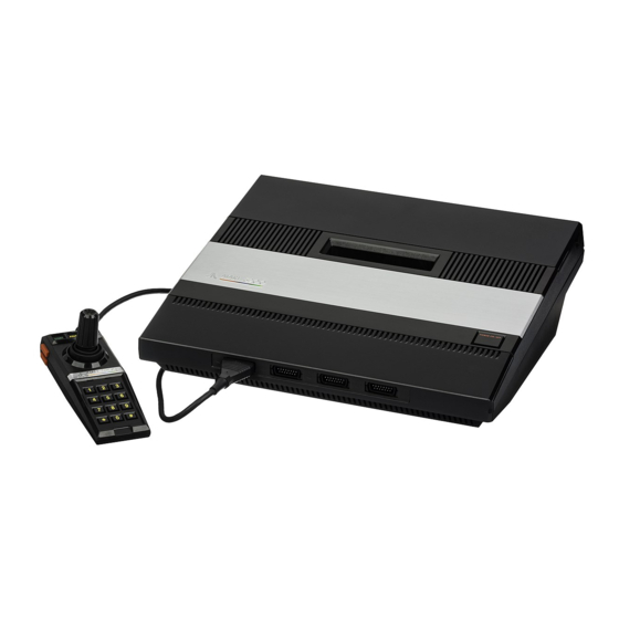
Page 11: Outer Case
Outer Case The outer case consists of a bottom and a top plastic cover which are held together by five Phillips-head screws. At the rear of the bottom plastic cover (Figure 1-2) is: a) an opening for access to the channel 2-3 switch b) a removable door which allows access for future development. -
Page 12: Microprocessor Chip Mpu
The PC Board consists of: • 28 Integrated Circuit Chips on PC Board Number CA018087; 26 Integrated Circuit Chips on PC Board Number CA020108; 24 Integrated Circuit Chips on PC Board Number CA021374. • a cartridge socket • an RF module •... -
Page 13: Alphanumeric Television Interface Controller
Alphanumeric Television Interface Controller (ANTIC) Alphanumeric Television Interface Controller (ANT Alphanumeric Television Interface Controller (ANT Alphanumeric Television Interface Controller (ANT The primary function of the Alphanumeric Television Interface Controller (ANTIC) chip is to get data from memory, independent of the processor, for display on the video screen. -
Page 14: Pot Keyboard Integrated Circuit (Pokey)
Figure 1-5. GTIA Pin Assignments POT Keyboard Integrated Circuit (POKEY) POT Keyboard Integrated Circuit (POKEY) POT Keyboard Integrated Circuit (POKEY) POT Keyboard Integrated Circuit (POKEY) The Pot Keyboard Integrated Circuit (POKEY) chip provides the interface between the game ports and the microprocessor. It also contains four semi- independent audio channels, each with its own frequency, noise, and volume control. -
Page 15: Switchbox
A switchbox is connected and mounted to the back of the television set. The switchbox that is used with the 4 – Port Models is different from other switchboxes manufactured by Atari and from the 2 – Port Mode1 5200. These differences include: 1) power for the Model 5200 supplied through the switchbox 2) two Select Switch functions. -
Page 16: Silkscreens And Schematics
SECTION 2 SECTION 2 SECTION 2 SECTION 2 SILKSCREENS AND SCHEMATICS SILKSCREENS AND SCHEMATICS SILKSCREENS AND SCHEMATICS SILKSCREENS AND SCHEMATICS On the following pages are representative silkscreens and schematics for the Model 5200. Minor variations in design may be encountered depending on the production date of the unit, but these schematics provide all details required for an in-depth understanding of all Model 5200 units. -
Page 17: Port 5200 Ca018087 Motherboard Silkscreen
Figure 2 – 1. 4 – Port 5200 CA018087 Motherboard Silkscreen CX5200 Field Service Manual... -
Page 18: Port 5200 Ca018087 Motherboard Schematic Part
Figure 2 2. 4 – Port 5200 CA018087 Motherboard Schematic Part 1 – CX5200 Field Service Manual... -
Page 19: Port 5200 Ca018087 Motherboard Schematic Part
Figure 2 – 3. 4 – Port 5200 CA018087 Motherboard Schematic Part 3 CX5200 Field Service Manual... -
Page 20: Port 5200 Ca018087 Motherboard Schematic Part 3
Figure 2 – 4. 4 – Port 5200 CA018087 Motherboard Schematic Part 3 CX5200 Field Service Manual... -
Page 21: Port 5200 Ca020108 Motherboard Silkscreen
Figure 2 – 5. 4 – Port 5200 CA020108 Motherboard Silkscreen CX5200 Field Service Manual... - Page 22 Figure 2 – 6. 4 – Port 5200 CA020108 Motherboard Schematic Part1 CX5200 Field Service Manual...
- Page 23 Figure 2 – 7. 4 – Port 5200 CA020108 Motherboard Schematic Part2 CX5200 Field Service Manual...
- Page 24 Figure 2 – 8. 4 – Port 5200 CA020108 Motherboard Schematic Part 3 CX5200 Field Service Manual...
-
Page 25: Port 5200 Ca021374 Motherboard Silkscreen
Figure 2 – 9. 2 – Port 5200 CA021374 Motherboard Silkscreen CX5200 Field Service Manual... -
Page 26: Port 5200 Ca021374 Motherboard Schematic Part
Figure 2 – 10. 2 – Port 5200 CA021374 Motherboard Schematic Part 1 CX5200 Field Service Manual... -
Page 27: Port 5200 Ca021374 Motherboard Schematic Part 2
Figure 2 – 11. 2 – Port 5200 CA021374 Motherboard Schematic Part 2 CX5200 Field Service Manual... -
Page 28: Port 5200 Ca021374 Motherboard Schematic Part
Figure 2 – 12. 2 – Port 5200 CA021374 Motherboard Schematic Part 3 CX5200 Field Service Manual... -
Page 29: Trakball Silkscreen
Figure 2 – 13. Trakball Silkscreen CX5200 Field Service Manual... -
Page 30: Trakball Schematic Part1
Figure 2 – 14. Trakball Schematic Part1 CX5200 Field Service Manual... -
Page 31: Trakball Schematic Part2
Figure 2 – 15. Trakball Schematic Part 2 CX5200 Field Service Manual... -
Page 32: Equipment Requirements
SECTION 3 SECTION 3 SECTION 3 SECTION 3 4 4 4 4 – – – – Port Port Port MODEL 5200 TESTI Port MODEL 5200 TESTI MODEL 5200 TESTI MODEL 5200 TESTING EQUIPMENT REQUIREMENTS You require six basic pieces of equipment in order to analyze failures in the Model 5200. -
Page 33: Power-Up Screen
NOTE: The Diagnostic Cartridge will cycle automatically only if the Port Board is inserted before the unit is turned on. POWER-UP SCREEN Figure 3-1 Power-Up Screen The Power-up screen appears in a few seconds. It displays information about the inner workings of the unit. This screen shows: The type of TIA in the unit. -
Page 34: Test Menu Screen
Warped - Ragged Picture In this failure, the power-up screen appears bent to one side with a ragged edge. The picture may roll or slide down and to the left of the screen. This means that the sync. signal broadcast by the GTIA is probably not functioning. Another possible cause is that the unit is not set on the same channel as the T.V. -
Page 35: Color Bars Screen
SAME COLOR REFERENCE BAR Figure 3-3 Color Bars Screen Diagnostic Flowchart Entry Point: Pg. 58. GREYBARS TEST • Purpose: To test the function of the luminescence lines (LM0, LM1, LM2) from the GTIA chip. • Format: Eight horizontal grey bars are displayed, going from black at the top to white at the bottom in even steps (see Figure 3-2 ). -
Page 36: Anyvideo Screen
ANYVIDEO SCREEN • Purpose: To test the video generation of the GTIA and ANTIC chips. Format: The screen should have a black background with eight vertical • bars. Half of the vertical bars should be narrow, and the other half much wider. -
Page 37: Softfire Signal
NOTE: Figure 3-6 shows a sample Pokey Adjust screen. The values on your screen may differ from those shown in Figure 3-6. POKEY SOFTFIRE TEST 1. Connect the oscilloscope to pin 16 of A7 (1V/div.; 10ms/div.). 2. Insert the controller into port 1. 3. - Page 38 Table 3-1 shows the defective component and/or the flowchart entry point which corresponds to the Failure Code number on the Error Summary. Table 3-1 Diagnostic Error Codes Failure Failure Reference Page # Code RAM - Chip 1 - U25 RAM Test, Pg. 3-10 RAM - Chip 2 - U24 "...
- Page 39 • Purpose: To test the 16K RAM chips for proper functioning. Format: This test takes approximately 10 seconds. At the end of this time • period, if the test has failed, a Failure Code number appears on the screen to signify which chip is defective. Swap out the chip corresponding to the Diagnostic Error Code (Table 3-1).
- Page 40 SECTION 3A TION 3A TION 3A TION 3A 2 2 2 2 – – – – PORT PORT MODEL 5200 TESTING MODEL 5200 TESTING PORT PORT MODEL 5200 TESTING MODEL 5200 TESTING EQUIPMENT REQUIREMENTS • You require seven basic pieces of equipment in order to analyse failures in the Model 5200 2 –...
-
Page 41: A-1 Power-Up Screen
POWER-UP SCREEN Figure 3A-1 Power-Up Screen The Power-up screen appears in a few seconds. It displays information about the inner workings of the unit. This screen shows: The type of TIA in the unit. NTSC appears if the GTIA is the proper one •... -
Page 42: Colour Bar Test
Warped - Ragged Picture In this failure, the power-up screen appears bent to one side with a ragged edge. The picture may roll or slide down and to the left of the screen. This means that the sync. signal broadcast by the GTIA is probably not functioning. Another possible cause is that the unit is not set on the same channel as the T.V. -
Page 43: Grey Bar Test
SAME COLOR REFERENCE BAR Figure 3A-3 Color Bars Screen Diagnostic Flowchart Entry Point: Pg. 84. GREY BAR TEST • Purpose: To test the function of the luminescence lines (LM0, LM1, LM2) from the GTIA chip. • Format: Eight horizontal grey bars are displayed, going from black at the top to white at the bottom in even steps (see Figure 3A-4 ). -
Page 44: Anyvideo Screen
ANYVIDEO SCREEN • Purpose: To test the video generation of the GTIA and ANTIC chips. Format: The screen should have a black background with eight vertical • bars. Half of the vertical bars should be narrow, and the other half much wider. -
Page 45: Error Summary
NOTE: Figure 3A-6 shows a sample Pokey Adjust screen. The values on your screen may differ from those shown in Figure 3A-6. If the unit cannot be adjusted or if values are out of range, proceed to the Flowchart Entry Point: Pg. 90. POKEY SOFTFIRE TEST 8. -
Page 46: Swapout Procedure
F – Some lines terminate with an F inside a circle. When this occurs, return to the beginning of the test sequence on page 32. N – Some lines terminate with an N inside a circle. When this occurs, call your Atari Repair Hotline. Inside California (800) 672-1466 Outside California (800) 538-1535 (300) 538-1536... - Page 47 Black Screen Troubleshooting Is there +5V on the output of VR1? Is there a 1.78975 MHz Is there a 1.78975 MHz signal on pin 30 of U5? signal on pin 30 of U5? Is there a 3.5795 MHz signal on pin 28 of U5? Is there a 3.5795 MHz Swapout U5 and/or U3 signal on pin 29 of U5?
- Page 48 Black Screen Troubleshooting (cont.) Are the following voltages on the pins of the transistor: Are voltages Replace Base 3.5V 3.5V correct? Transistor(s) Emitter 4.3V 4.3V Collector 1.2V 1.0V Replace Check for open, shorted or Does unit wrong value component in function? clock circuit Repair...
- Page 49 Black Screen Troubleshooting (cont.) Defective VR1or output Is there approximately short to ground 11-13V on the input of (possible chip) VR1? Is there approximately 0V Defective J1 or open on point 2 of the between point 1 of VR2 & schematic? point 2 of VR1 with cartridge in)
- Page 50 Black Screen Troubleshooting (cont.) PCB # Pin # Repair open between chip / Is there +5V to all chips? +5V or Ground. (See chart) (Check for bad socket) Defective U1 or other Reset 1,21 circuitry connected to U2 Is Pin 40 of U2 at 5V ? Pin40 Open Pin 36 of U2 to Is Pin 36 of U3 at 5V ?
- Page 51 Black Screen Troubleshooting (cont.) Open Trace RAM chip Pin Is there a data signal on 2 to U2 or Repair Pin 2 of U18 - U25? Replace defective RAM. If only one chip is missing Is there a data signal on signal, replace that chip.
- Page 52 Black Screen Troubleshooting (cont.) Is there a 4V p-p signal Swapout on Pin 15 of U18 - U25? Swapout: 1) U17 2) U14 or defective R133, C140, R68 & C55 CX5200 Field Service Manual...
- Page 53 Snowy Screen Troubleshooting Defective: 1) RF Cable Is there 10 to 12 volts 2) Switchbox on the core of J3? 3) Battery Eliminator Is C48 good? (do not short across) Defective: 1) L13 Repair Is there +5V on Pin 3 of 2) RF Module the RF Module? 3) Open between Pin 2...
- Page 54 Snowy Screen Troubleshooting (cont.) Is there 0V on the Defective Q8 or Q9 collector of Q8? Is there 13V on the base Defective: and 14 V on the emitter of 1) Q7 2) R55 3) R58 or open trace to collector of Q8. Defective Q7 Repair Replace...
- Page 55 Snowy Screen Troubleshooting (cont.) Does Pin 11 of U29 Is Pin 10 of Does unit (A26) toggle each U29 (A26) Replace Q10 work? time S2 is pressed? Open trace or Is there continuity defective resistor or Repair trace between pin 9 & 12 of capacity in circuitry U29 (A26) Does Pin 11 of U29...
- Page 56 Snowy Screen Troubleshooting (cont.) Repair Open Pin 3 VR2 to VCC2, Is there +5V on the +5B or +5F output of VR2? Replace If Pin 3 VR2 short to ground: Possible short in chips. Remove chips one-by-one and turn on unit. If modulation occurs, bad chip has been located.
-
Page 57: Power-Up Screen
Warped Ragged Picture Troubleshooting Manually set on Power-Up screen Is there +5V p-p signal on Is R22 good? the leg of R22 connected to Pin4 of A1? Mistuned or Is there +5V p-p signal on Open between Pin 4 defective RF Pin 4 of U1? of U1 &... - Page 58 Color Troubleshooting Manually set onto color bars pattern Is frequency of Y1 Replace Y1 3.5795 MHz? Defective: Does Pin 17 of U5 adjust between 0 and 6V when R8 is adjusted? With Pin 17 of U5 adjusted Defective U5 or C11 to 6V is there 4V p-p signal on pin 21 of U5? Defective C11 or open...
- Page 59 Color Troubleshooting (cont.) Is there a .4V p-p signal on Defective R28 or open the base of Q3? Trace R28 to Q3. Is there a 4V p-p signal on Is the signal present at Defective the collector of Q3? approximately 0V? Is there a 3V p-p signal Defective R30 betweenC9 and R31?
- Page 60 Gray Bars Troubleshooting Manually set the 5200 to the Gray Bars pattern. Defective R23, R24, Is there a +5V p-p signal on R25 or open the side of R23, R24, & between R23, R24 R25. or R25 and RF Connected to U1? Module pin 4.
-
Page 61: Pokey Adjust Test
Pot Control Line Troubleshooting Manually set the 5200 to the Pokey Adjust test. Can +CAV on defective port be adjusted between 4-6.4V by turning R132? ***NOTE*** Swapout U7 If you are servicing a unit containing PCB CA020108, chip designators have been changed from U to A. Do pot lines pass? From Error Code on chart below determine which line... -
Page 62: Port Test
Pot Control Line Troubleshooting (cont.) Swapout: ***NOTE*** 1) U5 If you are servicing a unit containing 2) U7 PCB CA020108, chip designators have been changed from U to A. Can +CAV be adjusted now? Check the voltages on Q11-Q14 and compare readings to the ones shown for the “A”... - Page 63 Trigger Line Troubleshooting (Bottom Fire Button) Defective: Is the U5 pin for the 1) U5 defective port at +5V with 2) U5 Socket everything unplugged 3) Cap on that line from the Port? See chart below. Plug in controller Defective controller. Is pin still at +5V? Push and hold bottom fire button...
- Page 64 Softfire (Top Fire Button) Troubleshooting Insert Diagnostic cartridge into console. Insert Game Controller into Port 1. Manually select Pokey adjust test. Are there 5V p-p Replace waveforms at U13 Are there 5V p-p waveforms Pins 9 & 10? at U13 Pins 1, 2, 4, & 5? Are there 5V p-p Replace Depress and hold softfire...
- Page 65 Keyboard Troubleshooting Is the failure on Port 1? Manually select Pokey Adjust Test Are there 5V p-p square waves on Pin 6 of U9 – U12? Are there5V p-p square Replace waves on Pin 9 & 10 of U9 – U12? Port 4 Port 2 Which port failed?
- Page 66 Keyboard Troubleshooting (cont.) Is there 0V on Pin 6 Replace Is there 0V on Pin 6 of U9 & U11? of U9 & U11? Swapout: Defective U5 or open traces from U5 to U27. Is the problem repaired? Repair Replace Check capacitors and resistors on Pins 1 –...
- Page 67 Keyboard Troubleshooting (cont.) Swapout: 1) U9 2) U12 Does Port 2 pass? Check capacitors and resistors on Pins 1 – 8 of Port 2 for proper value and operation. Replace if defective. ***NOTE*** If you are servicing a unit containing PCB CA020108, chip designators have been changed from U to A.
- Page 68 Keyboard Troubleshooting (cont.) Swapout: Does Port 3 pass? Check capacitors and resistors on Pins 1 – 8 of Port 3 for proper value and operation. Replace if defective. ***NOTE*** If you are servicing a unit containing PCB CA020108, chip designators have been changed from U to A.
- Page 69 Keyboard Troubleshooting (cont.) Swapout: 1) U10 2) U12 Does Port 4 pass? Check capacitors and resistors on Pins 1 – 8 of Port 4 for proper value and operation. Replace if defective. ***NOTE*** If you are servicing a unit containing PCB CA020108, chip designators have been changed from U to A.
- Page 70 Keyboard Troubleshooting (cont.) Does Port 4 pass? Swapout: 1) U27 2) U9 3) U11 Replace ***NOTE*** If you are servicing a unit containing PCB CA020108, chip designators have been changed from U to A. CX5200 Field Service Manual...
- Page 71 Audio Troubleshooting Can L1 be Is there a 4.5MHz signal adjusted to Adjust on the emitter of Q4? give a 4.5MHz reading? With audio test going is Replace: Is there +5VDC Swapout: Does audio there a series of changing 1) L1 on the collector 1) U7 work?
- Page 72 N – Some lines terminate with an N inside a circle. When this occurs, call you: Atari Repair Hotline. Inside California (800) 672-1466 Outside California (800) 538-1535 (300) 538-1536...
- Page 73 Black Screen Troubleshooting Is there +5V on the output of VR1? Is there a 1.78975 MHz Is there a 1.78975 MHz signal on pin 30 of A5? signal on pin 29 of A3? Is there a 3.5795 MHz signal on pin 28 of A5? Is there a 3.5795 MHz Swapout A5 and/or A3 signal on pin 29 of A5?
- Page 74 Black Screen Troubleshooting (cont.) Are the following voltages on the pins of the transistor: Are voltages Replace Base 3.5V 3.5V correct? Transistor(s) Emitter 4.3V 4.3V Collector 1.2V 1.0V Replace Check for open, shorted or Does unit wrong value component in function? clock circuit Repair...
- Page 75 Black Screen Troubleshooting (cont.) Defective VR1 or output Is there approximately short to ground 9V on the input of VR1? (possible chip) Defective J1 or open Is there approximately 9V between point CI1 and on point CI1 of the point CI2 with schematic? cartridge in.
- Page 76 Black Screen Troubleshooting (cont.) Repair open between chip / Is there +5V to all chips? +5V or Ground. (See chart) (Check for bad socket) Defective A1 or other Reset circuitry connected to A2 Is Pin 40 of A2 at 5V ? Pin40 Pin# Pin#...
- Page 77 Black Screen Troubleshooting (cont.) Open Trace RAM chip Pin Is there a data signal on 2 to A2 or Repair Pin 2 of A18 - A25? Replace defective RAM. If only one chip is missing Is there a data signal on signal, replace that chip.
- Page 78 Black Screen Troubleshooting (cont.) Swapout Is there a 4V p-p signal A15 or replace on Pin 15 of A18 - A25? defective C30-C33, L4-L6 Swapout: 1) A17 2) A14 or defective R133, C140, R68, L3 & C55 CX5200 Field Service Manual...
- Page 79 Snowy Screen Troubleshooting Defective: 1) RF Cable Is there 10 to 12 volts 2) Switchbox on the core of J3? 3) Battery Eliminator Is C48 good? (do not short across) Defective: 1) L13 Repair Is there +5V on Pin 3 of 2) RF Module the RF Module? 3) Open between Pin...
- Page 80 Snowy Screen Troubleshooting (cont.) Is there 0V on the Defective Q8 or Q9 collector of Q8? Is there 13V on the base Defective: and 14 V on the emitter of 1) Q7 2) R55 3) R58 or open trace to collector of Defective Q7 Repair...
- Page 81 Snowy Screen Troubleshooting (cont.) Does Pin 11 of A26 Does unit Is Pin 10 of toggle each time S2 Replace Q10 work? A26 at 0V? is pressed? Open trace or Is there continuity defective resistor or Repair trace between pin 9 & 12 capacity in circuitry of A26? Does Pin 11 of A26...
- Page 82 Snowy Screen Troubleshooting (cont.) Repair Open Pin 3 VR2 to VCC2, Is there +5V on the +5B or +5F output of VR2? Replace If Pin 3 VR2 short to ground: Possible short in chips. Remove chips one-by-one and turn on unit. If modulation occurs, bad chip has been located.
- Page 83 Warped Ragged Picture Troubleshooting Manually set on Power-Up screen Is there +5V p-p signal on Is R22 good? the leg of R22 connected to Pin4 of A1? Mistuned or Is there +5V p-p signal on Open between Pin 4 defective RF Pin 4 of A1? of A1 and R22 module or L12 or...
- Page 84 Color Troubleshooting Manually set onto color bars pattern Is frequency of Y1 Replace Y1 3.5795 MHz? Defective: Does Pin 17 of A5 adjust 1) R8 between 0 and 6V when R8 2) CR2 is adjusted? 3) CR3 With Pin 17 of A5 adjusted Defective A5 or C11 to 6V is there 4V p-p signal on pin 21 of A5?
- Page 85 Color Troubleshooting (cont.) Is there a .4V p-p signal on Defective R28 or open the base of Q3? Trace R28 to Q3. Is there a 4V p-p signal on Is the signal present at Defective the collector of Q3? approximately 0V? Is there a 3V p-p signal Defective R30 between C9 and R31?
- Page 86 Gray Bars Troubleshooting Manually set the 5200 to the Gray Bars pattern. Defective R23, R24, Is there a +5V p-p signal on R25 or open the side of R23, R24, & between R23, R24 R25. or R25 and RF Connected to A1? Module pin 4.
- Page 87 Audio Troubleshooting Can L1 be Is there a 4.5MHz signal adjusted to Adjust on the emitter of Q4? give a 4.5MHz reading? With audio test going is Replace: Is there +5VDC Swapout: Does audio there a series of changing 1) L1 on the collector 1) U7 work?
- Page 88 Trigger Line Troubleshooting (Bottom Fire Button) Defective: Is the A5 pin for the 4) A5 defective port at +5V with 5) A5 Socket everything unplugged 6) Cap on that line from the Port? See chart below. Plug in controller Defective controller. Is pin still at +5V? Push and hold bottom fire button...
- Page 89 Softfire (Top Fire Button) Troubleshooting Insert Diagnostic cartridge into console. Insert Game Controller into Port 1. Manually select Pokey adjust test. Are there 5V p-p Replace waveforms at A9 Are there 5V p-p waveforms Pins 9 & 10? at A9 Pins 1, 2, 4, & 5? Are there 5V p-p Replace Depress and hold softfire...
- Page 90 Pot Control Line Troubleshooting Manually set the 5200 to the Pokey Adjust test. Can +CAV on defective port be adjusted between 4-6.4V by turning R132? Swapout A7 Do pot lines pass? From Error Code on chart below determine which line is defective &...
- Page 91 Pot Control Line Troubleshooting (cont.) Swapout: 3) A5 4) A7 Can +CAV be adjusted now? Check the voltages on Q11-Q14 and compare readings to the ones shown for the “A” condition in the chart below. Does Pokey Replace transistor Are the readings correct? adjust pass? Defective component in Pokey adjust circuitry.
- Page 92 Keyboard Troubleshooting Is the failure on Port 1? Manually select Pokey Adjust Test Are there 5V p-p square Are there 5V p-p Replace waves on Pin 6 of square waves on A9 and A10? Pin 12 of A5? Are there 5V p-p square Replace waves on Pin 9 &...
- Page 93 Keyboard Troubleshooting (cont.) Is there +5VDC on Pins Replace Is there 0V on Pin 6 4, 5 & 14 of A27? of A9? Swapout: Defective A5 or open traces from A5 to A27. Is the problem repaired? Repair Replace Check capacitors and resistors on Pins 1 –...
- Page 94 Keyboard Troubleshooting (cont.) Swapout: 1) A10 2) A11 Does Port 2 pass? Check capacitors and resistors on Pins 1 – 8 of Port 2 for proper value and operation. Replace if defective. CX5200 Field Service Manual...
-
Page 95: Failures
SECTION 5 SECTION 5 SECTION 5 SECTION 5 4 4 4 4 – – – – PORT PORT 5200 SYMPTOM CHECKLIST 5200 SYMPTOM CHECKLIST PORT PORT 5200 SYMPTOM CHECKLIST 5200 SYMPTOM CHECKLIST The Symptom Cecklist is designed to assist the experienced technician arrive at a rapid diagnosis for model 5200 problems. - Page 96 SECTION 5A A A A SECTION 5 SECTION 5 SECTION 5 2 2 2 2 – – – – PORT PORT 5200 SYMPT 5200 SYMPTOM CHECKLIST OM CHECKLIST PORT PORT 5200 SYMPT 5200 SYMPT OM CHECKLIST OM CHECKLIST The Symptom Cecklist is designed to assist the experienced technician arrive at a rapid diagnosis for 2 –...
- Page 97 CX5200 Field Service Manual...
- Page 98 CX5200 Field Service Manual...
- Page 99 CX5200 Field Service Manual...
- Page 100 CX5200 Field Service Manual...
- Page 101 CX5200 Field Service Manual...
Need help?
Do you have a question about the CX 5200 and is the answer not in the manual?
Questions and answers