LG BP340 Service Manual
Hide thumbs
Also See for BP340:
- Owner's manual (62 pages) ,
- Simple manual (2 pages) ,
- Simple manual (2 pages)

Related Manuals for LG BP340


Summary of Contents for LG BP340
- Page 1 Internal Use Only Website http://biz.lgservice.com BLU-RAY DISC / DVD PLAYER SERVICE MANUAL MODEL: BP340 CAUTION BEFORE SERVICING THE UNIT, READ THE “SAFETY PRECAUTIONS” IN THIS MANUAL. P/NO : AFN76114583 MAY, 2014...
- Page 2 CONTENTS SECTION 1 ..SUMMARY SECTION 2 ..CABINET & MAIN CHASSIS SECTION 3 ..ELECTRICAL SECTION 4 ..REPLACEMENT PARTS LIST...
-
Page 3: Table Of Contents
SECTION 1 SUMMARY CONTENTS PRODUCT SAFETY SERVICING GUIDELINES FOR BLU-RAY DISC / DVD PLAYER PRODUCTS ..................1-3 SERVICING PRECAUTIONS .......................... 1-4 • GENERAL SERVICING PRECAUTIONS • INSULATION CHECKING PRODEDURE • ELECTROSTATICALLY SENSITIVE (ES) DEVICES HIDDEN KEY MODE ............................1-5 UPDATE GUIDE ............................... 1-6 SPECIFICATIONS ............................ -
Page 4: Product Safety Servicing Guidelines For Blu-Ray Disc / Dvd Player Products
When servicing this product, under no circumstances should the original design be modified or altered without permission from LG Corporation. All components should be replaced only with types identical to those in the original circuit and their physical location, wiring and lead dress must conform to original layout upon completion of repairs. -
Page 5: Servicing Precautions
SERVICING PRECAUTIONS CAUTION: Before servicing the BLU-RAY DISC / DVD PLAYER cov- Electrostatically Sensitive (ES) Devices ered by this service data and its supplements and addends, Some semiconductor (solid state) devices can be damaged read and follow the SAFETY PRECAUTIONS. easily by static electricity. -
Page 6: Hidden Key Mode
HIDDEN KEY MODE HIDDEN MODE AVAILABLE STATUS ENTRANCE KEY EXIT KEY DISPLAY RESULT OPTION Data editable (NO DISC||OPEN)&& EDIT EEPROM DATA PAUSE+1+4+7+2 PAUSE Option Values It shall be disable on MP (Home Menu OFF) version. FACTORY RESET DISPLAY SYSTEM (NO DISC||OPEN)&& 1+3+9+7+1+3+9+ SYSTEM (All of data have to be... -
Page 7: Update Guide
UPDATE GUIDE 1. USB TO UPDATE APP 2. USB TO UPDATE SERVO 1) Put the APP in the root of USB, and named as 1) Put the servo in the root of USB, and named as “LG_BD_9000M51.ROM” “H15SON.ROM” 2) Power on and get in the home menu, insert the 2) Power on and get in the home menu, insert the USB. -
Page 8: Specifications
SPECIFICATIONS • GENERAL Power Requirement AC 110~240 V, 50/60 Hz Power Consumption 12 W Dimensions (W× D× H) 260 mm x 198.5mm x 37 mm Net Weight (Approx.) 0.937 kg Operating Temperature 0 °C ~ 40 °C Operating Humidity -20 °C ~ 60 °C Standard Condition 25 °C, 65 % •... - Page 9 MEMO...
- Page 10 SECTION 2 CABINET & MAIN CHASSIS CONTENTS HOW TO REMOVE THE TOP CASE ......................2-2 EXPLODED VIEWS ............................2-4 1. CABINET AND MAIN FRAME SECTION ....................2-4 2. PACKING ACCESSORY SECTION ......................2-5...
-
Page 11: How To Remove The Top Case
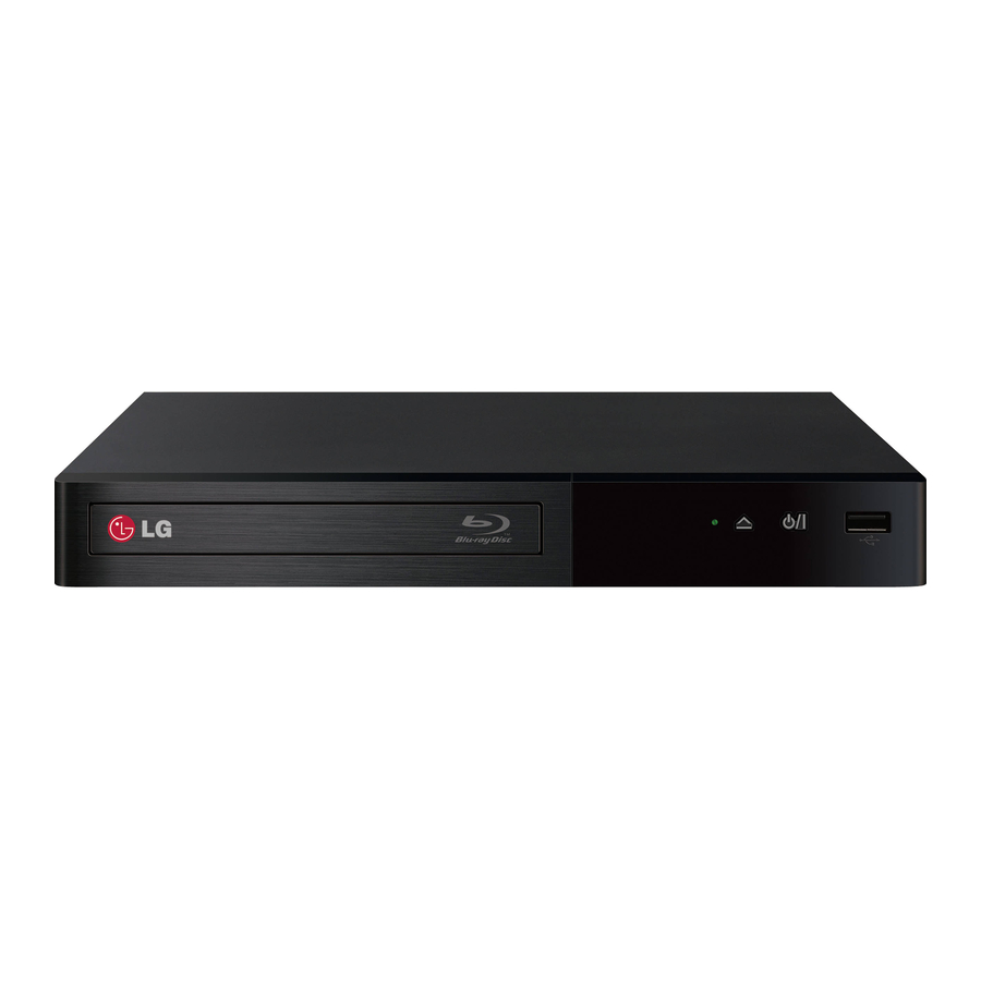
HOW TO REMOVE THE TOP CASE 1. Front view of the product It is a front view of the set. 2. Removing the top case/ back panel screws Remove the two screws that retain the top case of the back panel. - Page 12 3. Removing the top case 1) Lift 45 degrees back of the top case as shown in fi gure. 2) Press the arrow position to separate the top case and hook, and remove the bottom case and top case.
-
Page 13: Exploded Views
EXPLODED VIEWS 1. CABINET AND MAIN FRAME SECTION CABLE1 CABLE3 CABLE2 SMPS BOARD MAIN BOARD CABLE4 MODULE... -
Page 14: Packing Accessory Section
2. PACKING ACCESSORY SECTION 801 Instruction Ass’y 900 Remote Control 808 Battery 804 Bag 803A Packing (Pad2 Back) 803 Packing (Pad Front) 802 Box... - Page 15 MEMO...
- Page 16 SECTION 3 ELECTRICAL CONTENTS ONE POINT REPAIR GUIDE .......................... 3-2 1. NO BOOTING WHEN YOU TURN THE UNIT ON ................. 3-2 ELECTRICAL TROUBLESHOOTING GUIDE ....................3-5 1. SMPS TROUBLESHOOTING FLOW ..................... 3-5 2. UNIT POWER CHECK FLOW ........................ 3-6 3. UNIT CANNOT POWER ON ........................3-6 4.
-
Page 17: One Point Repair Guide
ONE POINT REPAIR GUIDE 1. NO BOOTING WHEN YOU TURN THE UNIT ON When you plug power cord and turn the unit on, LED light won’t turn green, the unit won’t output video and read disc normally. 1-1. Please check every output voltage. 1) Please check if output voltage 12 V from main board C92 is normal. - Page 18 ONE POINT REPAIR GUIDE NO BOOTING WHEN YOU TURN THE UNIT ON When you plug power cord and turn the unit on, LED light won’t turn green, the unit won’t output video and read disc normally. 1-2. Please check main board IC U1 signal and its peripheral circuit. 1) Please check if RESET_signal from main board C214 is normal.
- Page 19 ONE POINT REPAIR GUIDE NO BOOTING WHEN YOU TURN THE UNIT ON When you plug power cord and turn the unit on, LED light won’t turn green, the unit won’t output video and read disc normally. 1-3. Please check main board IC U2 & U3 signal and its peripheral circuit. 1) Please check if DDR_VREF 0.75 V from main board U2 &...
-
Page 20: Electrical Troubleshooting Guide
ELECTRICAL TROUBLESHOOTING GUIDE 1. SMPS TROUBLESHOOTING FLOW No +12 V output Replace the F501. Whether the F501 is normal? Whether the D501/ D502/ Replace the D501/ D502/ D503/ D504. D503/ D504 are normal? Replace the U501. Whether the U501 is normal? Replace the D505. -
Page 21: Unit Power Check Flow
ELECTRICAL TROUBLESHOOTING GUIDE 2. UNIT POWER CHECK FLOW TEST Whether power board Repair or replace power board. 12 V output is normal? Make sure the main board Repair or replace main board. don’t short. Whether main board Replace U5. 5 V output is normal? Whether main board Replace U4. -
Page 22: Remote Control Does Not Work
ELECTRICAL TROUBLESHOOTING GUIDE 4. REMOTE CONTROL DOES NOT WORK Remote control does not work. Whether remocon’s battery Replace battery for remote controller. is exhausted or not? Whether IR receiver power is OK? Replace IR1. IR1’s pin1, pin3 are about 5 V. Replace main board. -
Page 23: No Hdmi Output
ELECTRICAL TROUBLESHOOTING GUIDE 6. NO HDMI OUTPUT No HDMI output. Whether the HDMI cable is Connected TV and unit with HDMI cable. connected to the unit. Whether the TV display mode Adjust the TV display setting. or resolution is OK? Replace main board. -
Page 24: Cannot Read Usb Device Content
ELECTRICAL TROUBLESHOOTING GUIDE 8. CANNOT READ USB DEVICE CONTENT Cannot read USB device content. Whether the 5 V on front Fix the connection XP1 on front board to XP1 on main board. board XP1 pin8 is OK? Whether USB socket on front Replace USB socket P1. -
Page 25: Waveforms On System Test
WAVEFORMS ON SYSTEM TEST 1. POWER ON SYSTEM RESET SEQUENCE RESET active high must delay basis on all system power. 3.3V_STBY R181 R181 R176 R176 R179 R179 3.3K 3.3K RESET_ RESET_ RESET_ R177 R177 RESET_ R182 R182 C214 C214 2.7K 2.7K NPN_3DG3904M NPN_3DG3904M... -
Page 26: Block Diagram
BLOCK DIAGRAM 3-11... - Page 27 MEMO 3-12...
-
Page 28: Circuit Diagrams
DESIGN BE MODIFIED OR ALTERED WITHOUT DIFFER FROM THE ACTUAL CIRCUIT USED. THIS 2. Voltages are DC-measured with a digital voltmeter PERMISSION FROM THE LG CORPORATION. ALL WAY, IMPLEMENTATION OF THE LATEST SAFETY during Play mode. COMPONENTS SHOULD BE REPLACED ONLY WITH... -
Page 29: Smps - Key/ Led/ Usb Port/ Ir Circuit Diagram
2. SMPS - KEY/ LED/ USB PORT/ IR CIRCUIT DIAGRAM DuPont pin +12V +12V +12V +12V IROUT IROUT IROUT IROUT VSTB KEY1 KEY1 STANBY/ON STANBY/ON USB_GND USBP USBP USBP USBP USBM USBM USBM USBM VSCK KEY2 KEY2 OPEN/CLOSE OPEN/CLOSE USB_VCC USB_VCC USB_VCC USB_VCC... -
Page 30: Main - Power Source Circuit Diagram
3. MAIN - POWER SOURCE CIRCUIT DIAGRAM G5175 G5175 MODE 2.2UF 2.2UF 0.1uF/16V/X7R 0.1uF/16V/X7R V33P 3.3V_STBY 2.2UF 2.2UF 100K 100K PGOOD 2.2UF 2.2UF LDO(0.15A) LDO(0.15A) PVCC1_1 PVCC1_2 0.1uF/16V/X7R 0.1uF/16V/X7R 10UF 10UF 1.2V 0.1uF/16V/X7R 0.1uF/16V/X7R 2.2uH/3A 2.2uH/3A COMP1 LX1_1 LX1_2 10UF 10UF 2.2K/1% 2.2K/1%... -
Page 31: Main - Ddr3 #1 Circuit Diagram
4. MAIN - DDR3 #1 CIRCUIT DIAGRAM 1.5V 1.5V 0.1uF/16V/X7R 0.1uF/16V/X7R 0.1uF/16V/X7R 0.1uF/16V/X7R 10UF 10UF 0.1uF/16V/X7R 0.1uF/16V/X7R 0.1uF/16V/X7R 0.1uF/16V/X7R RDQ2 RDQ10 DDRVCCIO RDQ0 RDQ6 RDQ12 DDRVCCIO RDQ0 RDQ1 RDQ3 RDQ7 DDRVCCIO RDQ1 RDQ2 RDQ4 RDQ2 DDRVCCIO RDQ2 1.5V RDQ3 RDQ0 DDRVCCIO RDQ3 RDQ4... -
Page 32: Main - Ddr3 #2 Circuit Diagram
5. MAIN - DDR3 #2 CIRCUIT DIAGRAM 1.2V 1.2V DVCC12_K DVCC12_K AC12 RDQ0_B RDQ3_B RA0_B DVCC12_K RDQ0_B 22uF/6.3V/X5R 22uF/6.3V/X5R 0.1uF/16V/X7R 0.1uF/16V/X7R 0.1uF/16V/X7R 0.1uF/16V/X7R AC13 RDQ1_B RDQ7_B RA1_B 0.1uF/16V/X7R 0.1uF/16V/X7R 0.1uF/16V/X7R 0.1uF/16V/X7R DVCC12_K RDQ1_B AD13 RDQ2_B RDQ2_B RA2_B DVCC12_K RDQ2_B AE13 RDQ3_B RDQ6_B RA3_B... -
Page 33: Main - Hdmi Circuit Diagram
6. MAIN - HDMI CIRCUIT DIAGRAM AVDD33_VDAC AMUTE 3.3V AVDD33_VDAC AMUTE AOLRCK AOSDATA0 AVSS33_VDAC AOSDATA1 AOSDATA2 AOSDATA3 AOSDATA4 AVDD33_VDAC_R 3.3V AVDD33_VDAC_R SPDIF AMUTE AVSS33_VDAC_R AMUTE AVDD33_PLLGP 3.3V_STBY AVDD33_PLLGP VDACX_OUT VDACR_OUT VDACG_OUT VDACB_OUT AVSS33_PLLGP AVDD12_HDMI 1.2V AVDD12_HDMI_C AVDD12_HDMI_D AVDD33_HDMI Differential Signal ! 3.3V AVDD33_HDMI No Through Hole ! -
Page 34: Main - Usb Circuit Diagram
7. MAIN - USB CIRCUIT DIAGRAM 3.3V 3.3V 3.3V AVDD33_USB NC/10K NC/10K NC/10K NC/10K NC/10K NC/10K NC/10K NC/10K NC/10K NC/10K 3.3V DVCC33_IO AVDD33_USB AMUTE DVCC33_IO AMUTE C114 C114 C116 C116 DVCC33_IO AMUTE DVCC33_IO NC/0.1uF/16V/X7R NC/0.1uF/16V/X7R 0.1uF/16V/X7R 0.1uF/16V/X7R 0.1uF/16V/X7R 0.1uF/16V/X7R NFCEN DVCC33_IO AVSS33_USB NFWEN... -
Page 35: Main - Micom Circuit Diagram
8. MAIN - MICOM CIRCUIT DIAGRAM 3.3V_STBY GPIO3 3.3V_STBY GPIO0 DVCC33_IO_STB GPIO0 DVCC33_IO_STB GPIO1 DVCC33_IO_STB GPIO1 UARXD UARXD UARXD UATXD UATXD VSTB VSTB VSTB VSTB AVDD33_LDO VDATA VDATA VDATA AVDD33_LDO VDATA VCLK VCLK VCLK VCLK LCDRD R105 R105 VOUTD3 TP29 TP29 LCDRD VOUTD3... -
Page 36: Main - Front End Circuit Diagram
9. MAIN - FRONT END CIRCUIT DIAGRAM V14REF C148 C148 2.2UF 2.2UF A1.2V V14REF AVDD12_1 AVDD12_1 KEM-480AAA FVREF FVREF AVDD12_2 HAVC FEGIO10 HAVC TP41 TP41 HAVC TRINA FEGIO11 TP42 TP42 TRINA RFO+,RFO-,INA,INB,INC,IND signal trace length should <6cm C150 C150 TRINB C147 C147 TRINB... -
Page 37: Main - Motor Drive Circuit Diagram
10. MAIN - MOTOR DRIVE CIRCUIT DIAGRAM MOTOR DRIVER TI2060A M12V_T TPIC_B+ SLED1_P TPIC_B- LDO_FB SLED1_N LINFB LDO_9VG P12V_SLD LIN9VG TPIC_A+ TP33 TP33 SLED2_P TEST C119 C119 C122 C122 SLED2_N PGND_2 AGND 4.7uF 4.7uF 0.1uF/16V/X7R 0.1uF/16V/X7R C124 0.1uF/16V/X7R C124 0.1uF/16V/X7R C10V C120 0.1uF/25V/X7R C120 0.1uF/25V/X7R... -
Page 38: Circuit Voltage Chart
CIRCUIT VOLTAGE CHART 1. ICs Location Location Location Location Location PLAY Location PLAY Part SPEC Part SPEC Part SPEC SPEC(V) Voltag Voltage SPEC(V) Voltage SPEC(V) Voltage SPEC(V) Voltage Voltage U1 13-MT8551-PHAG0 U2 13-NT5CB1-28M11 U3 13-NT5CB6-4M12 U1.K9 1.15V-1.25V 1.20 U1.W18 1.45V-1.6V 1.50 U1.H25 1.45V-1.6V... -
Page 39: Trs & Fets
2. TRs & FETs Location PLAY Location PLAY Location PLAY Part SPEC Part SPEC SPEC(V) Voltage SPEC(V) Voltage Transistor Part SPEC U4 13-G5175R-V1U3 (C) Voltage (E) Voltage (B) Voltage U11 13-TPIC20V-60A3 G5175RV1U TPIC2060A PMU - MAIN PCB Main board 5.15 5.15 Motor DriVer - MAIN PCB Main board... -
Page 40: Connectors
MEMO 5. CONNECTORS Location PLAY Part SPEC SPEC(V) Voltage XP1-PIN1 11.8V-12.8V 12.28 XP1-PIN2 XP1-PIN3 4.5V-5.5V 4.74 XP1-PIN4 4.5V-5.5V 5.11 XP1-PIN5 XP1-PIN6 0-1V XP1-PIN7 0-1V Dupont socket (XP1) PITCH=2MM (POWER PCB - MAIN PCB) XP1-PIN8 4.5V-5.5V 5.08 XP1-PIN9 3V-3.5V 3.363 XP1-PIN10 3V-3.5V 3.363 XP1-PIN11... -
Page 41: Printed Circuit Board Diagrams
PRINTED CIRCUIT BOARD DIAGRAMS 1. MAIN P.C. BOARD (TOP VIEW) (BOTTOM VIEW) 3-39 3-40... -
Page 42: Smps P.c. Board
2. SMPS P.C. BOARD (TOP VIEW) (BOTTOM VIEW) 3-41 3-42... - Page 43 MEMO MEMO 3-43 3-44...
Need help?
Do you have a question about the BP340 and is the answer not in the manual?
Questions and answers