Table of Contents
Advertisement
Table Of Contents
Service Manual
COVER
1 Before Repairs
TOP NEXT
2 Protection Circuitry
3 Accessories
AD0002043C2
4 Caution for AC Main
Leads
5 Location of Controls
6 Operation Checks and
Component
ReplacementProcedures
6.1 Checking for the AC IN
P.C.B.
Tuner/Amplifier
6.2 Checking for the
operation P.C.B.
SA-EH560
6.3 Checking for the main P.
C.B.
Colour
6.4 Replacement for the
regulator transistor
(S).....................Silver Type
6.5 Replacement for the
power IC
Areas
7 To Supply Power Source
8 Self-Diagnostic Mode
(E).....................Europe.
8.1 To display the
malfunction code
(EB)..................Great Britain.
8.2 To return to the normal
display
(EG)..................Germany, Italy, France, Netherlands and Denmark.
8.3 Display contents
8.3.1 U70 CD, U70 DECK
(displayed automatically)
8.3.2 F61
9 Schematic Diagram Notes
10 Schematic Diagram
11 Printed Circuit Board
Diagram
12 Type Illustration of ICs,
Transistors and Diodes
13 Wiring Connection
Diagram
14 Terminal Function of ICs
14.1 IC901
(LC8A524A5N28):System
Control/FL Drive
15 Block Diagram
16 Replacement Parts List
17 Cabinet Parts Location
18 Packaging
Advertisement
Table of Contents

Related Manuals for Technics SA-EH560


Summary of Contents for Technics SA-EH560
- Page 1 6 Operation Checks and Component ReplacementProcedures 6.1 Checking for the AC IN P.C.B. Tuner/Amplifier 6.2 Checking for the operation P.C.B. SA-EH560 6.3 Checking for the main P. C.B. Colour 6.4 Replacement for the regulator transistor (S).....Silver Type 6.5 Replacement for the...
- Page 2 © 2000 Matsushita Electric Industrial Co., Ltd. All rights reserved. Unauthorized copying and distribution is a violation of law.
-
Page 3: Table Of Contents
Table Of Contents COVER 1 Before Repairs 2 Protection Circuitry 3 Accessories 4 Caution for AC Main Leads 5 Location of Controls 6 Operation Checks and Component ReplacementProcedures 6.1 Checking for the AC IN P.C.B. 6.2 Checking for the operation P.C.B. 6.3 Checking for the main P.C.B. - Page 4 9 Schematic Diagram Notes 10 Schematic Diagram 11 Printed Circuit Board Diagram 12 Type Illustration of ICs, Transistors and Diodes 13 Wiring Connection Diagram 14 Terminal Function of ICs 14.1 IC901 (LC8A524A5N28):System Control/FL Drive 15 Block Diagram 16 Replacement Parts List 17 Cabinet Parts Location 18 Packaging...
-
Page 5: Service Manual
Service Manual TOP NEXT AD0002043C2 Tuner/Amplifier SA-EH560 Colour (S).....Silver Type Areas (E).....Europe. (EB)....Great Britain. (EG)....Germany, Italy, France, Netherlands and Denmark. - Page 6 © 2000 Matsushita Electric Industrial Co., Ltd. All rights reserved. Unauthorized copying and distribution is a violation of law.
-
Page 7: Before Repairs
1 Before Repairs TOP PREVIOUS NEXT 1. Turn off the power supply. Using a 10Ω, 10 W resistor, connect both ends of power supply capacitors (C701, C703 and C702, C704) in order to discharge the voltage. 2. Before turning the power supply on, after completion of repair, slowly apply the primary voltage by using a power supply voltage controller to make sure that the consumed current at 50 Hz in NO SIGNAL mode should be shown below with respectto supply voltage 230/240 V. -
Page 8: Protection Circuitry
2 Protection Circuitry TOP PREVIOUS NEXT The protection circuitry may have operated if either of the following conditions is noticed: No sound is heard when the power is switched ON. Sound stops during a performance. The functions of this circuitry is to prevent circuitry damage if, for example, the positive and negative speaker connection wires are shorted, or if speaker system with an impedance less than the indicated rated impedance of this unit are used. -
Page 9: Accessories
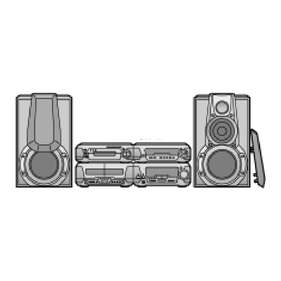
3 Accessories TOP PREVIOUS NEXT AC power supply cord for (E),(EG) areas/(RJA0019-X)......1 pc. AC power supply cord for (EB) area/(RJA0053-2X)......1 pc. AM loop antenna set/(RSA0022-J)......1 pc. FM indoor antenna/(RSA0007)......1 pc. Speaker cords/(REE0499)......2 pcs./(REE0984)......2 pcs./ (REE0985)......2 pcs. Remote control transmitter/(RAK-EHA29WH).....1 pc. Remote control batteries/(R6/LR6,“AA”, UM-3)....2 pcs. - Page 10 Note: These are available on sales route. Antenna plug adaptor for (EB) area only/(SJP9009)......1 pc. •@ TOP PREVIOUS NEXT...
-
Page 11: Caution For Ac Main Leads
4 Caution for AC Main Leads TOP PREVIOUS NEXT... -
Page 12: Location Of Controls
5 Location of Controls TOP PREVIOUS NEXT •@ TOP PREVIOUS NEXT... -
Page 13: Operation Checks And Component Replacementprocedures
6 Operation Checks and Component Replacement/Procedures TOP PREVIOUS NEXT This section describes procedures for checking the operation of the major printed circuit boards and replacing the main components. For reassembly after operation checks or replacement, reverse the respective procedures. Special reassembly procedures are described only when required. -
Page 14: Checking For The Ac In P.c.b
6.1 Checking for the AC IN P.C.B. TOP PREVIOUS NEXT Check the AC IN P.C.B. as shown below. •@ TOP PREVIOUS NEXT... -
Page 15: Checking For The Operation P.c.b
6.2 Checking for the operation P.C.B. TOP PREVIOUS NEXT Follow the (Step 1) (Step 3) of item 6.1. Check the operation P.C.B. as shown below. - Page 16 •@ TOP PREVIOUS NEXT...
-
Page 17: Checking For The Main P.c.b
6.3 Checking for the main P.C.B. TOP PREVIOUS NEXT Follow the (Step 1) (Step 3) of item 6.1. Follow the (Step 1) (Step 6) of item 6.2. - Page 19 Check the main P.C.B. as shown below. •@ TOP PREVIOUS NEXT...
-
Page 20: Replacement For The Regulator Transistor
6.4 Replacement for the regulator transistor TOP PREVIOUS NEXT Follow the (Step 1) (Step 3) of item 6.1. •@ TOP PREVIOUS NEXT... -
Page 21: Replacement For The Power Ic
6.5 Replacement for the power IC TOP PREVIOUS NEXT Follow the (Step 1) (Step 3) of item 6.1. Follow the (Step 1) (Step 6) of item 6.2. Follow the (Step 1) (Step 10) of item 6.3. •@ TOP PREVIOUS NEXT... -
Page 22: To Supply Power Source
This unit SA-EH560 is designed to operate on power supplied form system connected./For system connection, refer to Fig. 7-1. Fig. 7-1. When the unit SA-EH560 has to test and service alone, use the following method to supply power source. 1. Short the section between W902A Pin 3 C740 (-) (GND). - Page 23 Notes: Use only this method when checking the voltage etc../In case of checking the operations, use the system connections to supply power source. •@ TOP PREVIOUS NEXT...
-
Page 24: Self-Diagnostic Mode
8 Self-Diagnostic Mode TOP PREVIOUS NEXT This unit is equipped with a self-diagnostic function which, in the event of a malfunction, automatically displays a code indicating the nature of the malfunction. Use this self-diagnostic function when servicing the unit. 8.1 To display the malfunction code 8.2 To return to the normal display 8.3 Display contents 8.3.1 U70 CD, U70 DECK(displayed automatically) -
Page 25: To Display The Malfunction Code
8.1 To display the malfunction code TOP PREVIOUS NEXT U70 CD:/U70 DECK: Automatically displays on the tuner/amplifier when a malfunction occurs. Refer to Fig. 8-1. F61: Automatically displays on the tuner/amplifier when a malfunction occurs. Refer to Fig. 8-1. Fig. 8-1. •@... -
Page 26: To Return To The Normal Display
8.2 To return to the normal display TOP PREVIOUS NEXT For U70 CD/U70 DECK 2. Press an any operation button on the tuner/amplifier. 3. To re-display the code, switch the power off (POWER STANDBY button), and then switch power back on again For F61 5. -
Page 27: Display Contents
8.3 Display contents TOP PREVIOUS NEXT 8.3.1 U70 CD, U70 DECK(displayed automatically) 8.3.2 F61 •@ TOP PREVIOUS NEXT... -
Page 28: U70 Cd, U70 Deck(Displayed Automatically)
8.3.1 U70 CD, U70 DECK/(displayed automatically) TOP PREVIOUS NEXT Problem or condition A bus-line communications error has occurred as a result of the flat cables being inserted incorrectly, thus preventing the system from operating. 1. If U70 is displayed on the tuner/amplifier, the tape deck or CD Player cannot be operated by remote control. - Page 29 4. Breakage of flat cable. (Check and replace.) 5. If the problem is not corrected by items 1 and 2 above, this indicates a faulty IC. SA-EH560: IC901 (LC8A524A5N28) SL-EH560: IC451 (M38504M6200F) RS-EH760: IC701 (M38503M2400F) Check these ICs and replace.
- Page 30 When the power switch is switched on, it automatically switches back off, making it impossible to switch power on. Correction procedure Faulty Tuner/Amplifier (SA-EH560) output IC (IC601). (When a DC voltage is applied to speaker terminals.) •@ TOP PREVIOUS NEXT...
-
Page 31: Schematic Diagram Notes
9 Schematic Diagram Notes TOP PREVIOUS NEXT This schematic diagram may be modified at any time with the development of new technology. Notes: S901: Power Standby/on switch ( S902: ECO mode switch (MODE) S903: Clock/timer, demo switch/(CLOCK/TIMER, DEMO) S904: Play timer/record timer switch/( PLAY/ REC) S905:... - Page 32 S907: Set switch (SET) S908: Source input switch (INPUT SELECTOR) S910: Tuning down switch (TUNING, S911: Tuning up switch (TUNING, S912: Tuner/band switch (TUNER/BAND) S913: Super woofer switch (S.WOOFER) S914: RDS display mode PS switch/(RDS DISP MODE-PS)/ [For (E),(EG) areas] S915: RDS display mode PTY switch/(RDS DISP MODE-PTY)/ [For (E),(EG) areas]...
- Page 33 No mark : Power ON (FM or AM) Important safety notice: Components identified by mark have special characteristics important for safety. Furthermore, special parts which have purposes of fire-retardant (resistors), high-quality sound (capacitors), low-noise (resistors), etc. are used. When replacing any of components, be sure to use only manufacturer’s specified parts shown in the parts list.
- Page 34 : FM OSC signal line : AM signal line : AM OSC signal line : Source signal line : Low sp. drive signal line •@ TOP PREVIOUS NEXT...
-
Page 35: Schematic Diagram
10 Schematic Diagram TOP PREVIOUS NEXT •@ TOP PREVIOUS NEXT... -
Page 36: Printed Circuit Board Diagram
11 Printed Circuit Board Diagram TOP PREVIOUS NEXT •@ TOP PREVIOUS NEXT... -
Page 37: Type Illustration Of Ics, Transistors And Diodes
12 Type Illustration of ICs, Transistors and Diodes TOP PREVIOUS NEXT •@ TOP PREVIOUS NEXT... -
Page 38: Wiring Connection Diagram
13 Wiring Connection Diagram TOP PREVIOUS NEXT •@ TOP PREVIOUS NEXT... -
Page 39: Terminal Function Of Ics
14 Terminal Function of ICs TOP PREVIOUS NEXT 14.1 IC901 (LC8A524A5N28):System Control/FL Drive •@ TOP PREVIOUS NEXT... -
Page 40: Ic901 (Lc8A524A5N28):System Control/Fl Drive
14.1 IC901 (LC8A524A5N28):/System Control/FL Drive TOP PREVIOUS NEXT Pin No. Terminal Name Function CHECK O Clock check signal output LC72 DI O PLL data signal output LC72 CE O Chip enable signal output LC72 DO/ST IF count data/stereo detect signal input LC72 CK O Clock signal output Not used, open... - Page 41 REMOCON Remote control signal input Not used, open O Grid signal output Not used, open O Segment signal output VDD3 Power supply terminal O Segment signal output Power supply terminal (negative) O Segment signal output VDD4 Power supply terminal O Segment signal output REG IN0 Area select signal input REG IN1...
- Page 42 SH DO O Serial communication signal to Sound Processor (Data signal output) SH DI Serial communication signal to Sound Processor (Data signal input) SH CK Serial communication signal to Sound Processor (Clock signal input) E DET Unusual condition detect signal input CR TIMER I/O TIME CONSTANT terminal Station detector signal input from tuner circuit...
-
Page 43: Block Diagram
15 Block Diagram TOP PREVIOUS NEXT •@ TOP PREVIOUS NEXT... -
Page 44: Replacement Parts List
16 Replacement Parts List TOP PREVIOUS NEXT Notes: Important safety notice: Components identified by mark have special characteristics important for safety. Furthermore, special parts which have purposes of fire-retardant (resistors), high-quality sound (capacitors), low-noise (resistors), etc. are used. When replacing any of components, be sure to use only manufacture’s specified parts shown in the parts list. - Page 45 FOOT RING RKF0606A-K BACK GRILL RKW0581-1V FL WINDOW RMN0427 CABLE HOLDER RYP0946B-S FRONT PANEL (EB) RYP0946G-S FRONT PANEL (E,EG) 12-1 RGB0025-A TECHNICS BADGE SHG1654 RUBBER XTB3+10JFZ SCREW XTB3+8JFZ SCREW XTW3+15T SCREW XTBS3+8JFZ1 SCREW RLBT4001-N FERAITO COA RMN0582 PT HOLDER SHR9112...
- Page 46 RQT5352-D OPERATING INSTRUCTIONS (EG)/<IC> RQT5353-H OPERATING INSTRUCTIONS (EG)/<ID> RSA0007 FM INDOOR ANTENNA RSA0022-J AM LOOP ANTENNA SJP9009 ANT.ADAPTOR (EB) RQCA0736 SETTING GUIDE (EB) C151 ECEA1CKS100 16V 10U (E,EG) C152 ECBT1H331KB5 50V 330P (E,EG) C153 ECBT1H102KB5 50V 1000P (E,EG) C154 ECBT1H561KB5 50V 560P (E,EG) C155...
- Page 47 C631,32 ECBT1H473KB5 50V 0.047U C635-37 ECBT1H473KB5 50V 0.047U C639-42 ECBT1H102KB5 50V 1000P C647-50 ECBT1H102KB5 50V 1000P C655,56 ECA1CAK100XB 16V 10U C659,60 ECA1CAK100XB 16V 10U C666 ECBT1H473KB5 50V 0.047U C701 ECA1VM472E 35V 4700U C702,03 ECA1VM562E 35V 5600U C704 ECA1VM472E 35V 4700U C705 ECBT1H103KB5 50V 0.01U...
- Page 48 C761 ECQE1104KF3 100V 0.1U C791 ECKWRS102MBC 1000P C901 EEAFC0J101B 6.3V 100U C902 RCE1AM102BV 10V 1000U C903,04 ECBT1H103KB5 50V 0.01U C905 ECBT1H102KB5 50V 1000P C907,08 ECBT1H471KB5 50V 470P C909 ECBT1H102KB5 50V 1000P C910 ECBT1H200JC5 50V 20P C911 ECBT1H180J5 50V 18P C912 ECBT1H104KB5 50V 0.1U C913...
- Page 49 D500 MA165 DIODE D551,52 MA165 DIODE D555 MA4100M DIODE D558 MA165 DIODE D563 MA165 DIODE D601,02 SB360L6508 DIODE D607 1SS291TA DIODE D657-59 MA165 DIODE D701-04 1N5402BF DIODE D705 RL1N4003N02 DIODE D711 RL1N4003N02 DIODE D715 MA165 DIODE D717-20 RL1N4003N02 DIODE D721 MA4300M DIODE D723...
- Page 50 D933 MA165 DIODE (E,EG) D951 LNJ301MPUJAD D954 SELS5923C D956 SELS5923C D961 MA4075M DIODE D973 MA4030M DIODE D974 MA165 DIODE XBA2C10TB0 FUSE FL901 RSL0298-F IC151 LC72721NMTLM (E,EG) IC601 RSN311W64A IC901 LC8A524A5N28 JK601 ,02 RJH5603-1J 6P SP TANSI JK701 SJS9236 JACKAC INLET JK903 RJJ37TN02-C JACK,HEADPHONE...
- Page 51 RPN1194 PAD(SA) RPN1196 PAD(SH) RPN1203 PAD(SL) SPP740-1 SHEET RPF0139 PROTECTION BAG(F.B.) PCB1 REP2964D-M MAIN PCB (E,EG)/[RTL] PCB1 REP2964L-M MAIN PCB (EB) [RTL] PCB2 REP2966D-S SUB PCB (E,EG)/[RTL] PCB2 REP2966E-S SUB PCB (EB) [RTL] Q503 2SC3327A TRANSISTOR Q551 2SA1995RSTA TRANSISTOR Q554 2SA1995RSTA TRANSISTOR Q555...
- Page 52 R151,52 ERDS2FJ102 1/4W 1K (E,EG) R153,54 ERDS2FJ104 1/4W 100K (E,EG) R155 ERDS2FJ121 1/4W 120 (E,EG) R158 ERDS2FJ102 1/4W 1K (E,EG) R229,30 ERDS2FJ102 1/4W 1K R509-12 ERDS2FJ390 1/4W 39 R544 ERDS2FJ103 1/4W 10K R546,47 ERDS2FJ392 1/4W 3.9K R548 ERDS2FJ102 1/4W 1K R551 ERDS2FJ183 1/4W 18K...
- Page 53 R628 ERDS2FJ223 1/4W 22K R631,32 ERDS2FJ392 1/4W 3.9K R635 ERDS2FJ222 1/4W 2.2K R637 ERDS2FJ153 1/4W 15K R638 ERDS2FJ683 1/4W 68K R639,40 ERDS1FJ100 1/2W 10 R641,42 ERD2FCG100 1/4W 10 R643,44 ERDS1FJ100 1/2W 10 R645,46 ERD2FCG100 1/4W 10 R647,48 ERDS2FJ2R2 1/4W 2.2 R649,50 ERDS1FJ100 1/2W 10...
- Page 54 R768 ERDS2FJ101 1/4W 100 R770 ERDS2FJ104 1/4W 100K R771 ERDS2FJ222 1/4W 2.2K R772 ERDS2FJ223 1/4W 22K R773,74 ERDS1FJ180 1/2W 18 R776 ERDS2FJ103 1/4W 10K R777 ERDS2FJ102 1/4W 1K R791,92 RSFMB40KT-L FUSE PROTECTOR R793 ERDS2FJ1R0 1/4W 1 R794 ERDS2FJ473 1/4W 47K R795 ERDS2FJ392 1/4W 3.9K...
- Page 55 R934-36 ERDS2FJ101 1/4W 100 R937 ERDS2FJ103 1/4W 10K R939 ERDS2FJ152 1/4W 1.5K R943 ERDS2FJ101 1/4W 100 R944 ERDS2FJ222 1/4W 2.2K R945 ERDS2FJ101 1/4W 100 R946 ERDS2FJ102 1/4W 1K R947,48 ERDS2FJ104 1/4W 100K (EB) R949 ERDS2FJ472 1/4W 4.7K R950 ERDS2FJ101 1/4W 100 R951 ERDS2FJ334 1/4W 330K...
- Page 56 S901-08 EVQ11G05R S910-13 EVQ11G05R S914,15 EVQ11G05R (E,EG) T701 RTP2M5B018 POWER TRANSFORMER T702 RTP1H3E001 POWER TRANSFORMER VR901 EVQVBXFK124B V.R. X151 RSXC4M33S02T OSCILLATOR X901 EF0EC6004T4 OSCILLATOR X902 RSXD32K7S02 OSCILLATOR Z120 RAN0005EM-1 TUNER UNIT Z701 ERZV10V511CS COMPONENT COMBINATION Z901 RCDGP1U28XD REMOTE SENSOR •@ TOP PREVIOUS NEXT...
-
Page 57: Cabinet Parts Location
17 Cabinet Parts Location TOP PREVIOUS NEXT •@ TOP PREVIOUS NEXT... -
Page 58: Packaging
18 Packaging TOP PREVIOUS •@ TOP PREVIOUS... - Page 61 Z120 TUNER UNIT (RAN0005EM) FM ANT AM ANT +B(FM) RF AMP MIXER COIL COIL +B(FM) FM IF FM / AM I F AMP, +B(FM) BUFFER DET / AM OSC, FM OSC MIX / FM MPX (LA1833MN) +B(FM) FM:ON DECODER BUFEER PHASE STEREO PILOT...
- Page 62 W501 TUNER L/C TUNER R A.GND MID Lch IN MID Rch IN DC 10V TW Lch IN TW Rch IN To SOUND PROCESSOR BLOCK DIAGRAM -7.5V V.GND D.GND CS/REQ DATA CS.GND SH FL1 From POWER TRANSFORMER SH FL2 SYNC LC8A524A5N28 IC901 SYSTEM CONTROL / FL DRIVE...
- Page 63 Q605 (Q606) MUTING For [E,EG] areas. LC72721NMTLM IC151 RDS SIGNAL DEMODULATOR VREF FLOUT 3,13 CLOCK RECOVERY REFERENCE (57kHz) (1187.5Hz) VOLTAGE 4,12 VREF RDCL 57kHz DATA MPX IN ANTIALIASING SMOOTHING RDDA DECODER FILTER FILTER (SCF) CLK(4.332MHz) RDS-ID RDS-ID DETECT OSC/DIVIDER TEST XOUT STDBY X151...
- Page 64 HEADPHONES RSN311W64A IC601 POWER AMP Q911 (18) MUTING (Q912) D974 Q902,961 MUTING CONT D601 POWER CONTROL CIRCUIT (25) HIGH (6 ) (12) SPEAKERS (To SB-EH560) (6 ) (22) Q503,558 (6 ) SWITCH- POWER CONTROL/ PROTECTION CIRCUIT D906 D907 Q601,602 D602 SWITCH- Q551,554,555 SIGNAL...
- Page 65 Q702,705 REGULATOR D702,704, T701 752,754,755 D701,703, 751,753 D956 (TRI-AMPLIFIER) Q703,704 REGULATOR Q723 RL701 AC IN Q706 L701 SWITCH- +B11 REGULATOR Q701 RL702 Z701 REGULATOR Q709 POWER RELAY DRIVE Q708 SWITCH- SYNC D717~720 Q711,725 Q791 REGULATOR RELAY DRIVE Q707 D705 REGULATOR D711 D902 D901...
- Page 66 SCHEMATIC DIAGRAM-1 NOTE: :NEGATIVE VOLTAGE LINE The number which noted at the connectors on the schematic diagram as "SCHEMATIC DIAGRAM-1" or "SCHEMATIC DIAGRAM-2" :SOURCE SIGNAL LINE OPERATION CIRCUIT indicates the schematic diagram serial number located on the left corner in the schematic diagram. -27V FL901 (RSL0298-F) FL DISPLAY...
- Page 67 SCHEMATIC DIAGRAM-2 :POSITIVE VOLTAGE LINE :NEGATIVE VOLTAGE LINE B C D F G H I J K L M N O P Q R 5.2V X901 R953 (6MHz) R951 C910 330K C911 -27V -26.9V 5.2V REMOCON -21.8V 2.6V RDS DATA -25V -21.7V 2.5V...
- Page 68 SCHEMATIC DIAGRAM-3 OPERATION CIRCUIT :POSITIVE VOLTAGE LINE :NEGATIVE VOLTAGE LINE :SOURCE SIGNAL LINE 5.2V VR901 Z901 EVQVBXFK124B RCDGP1U28XD (VOLUME) (REMOTE SENSOR) R946 R945 R962 R943 R961 W902B A B C For [EB] area. R947 100K R948 100K For [E,EG] areas. IC151 LC72721NMTLM RDS SIGNAL...
- Page 69 SCHEMATIC DIAGRAM-4 :POSITIVE VOLTAGE LINE :FM SIGNAL LINE :SOURCE SIGNAL LINE MAIN CIRCUIT :NEGATIVE VOLTAGE LINE :AM SIGNAL LINE :LOW SP.DRIVE SIGNAL LINE C655 R687 R601 16V10 4.7K C656 R688 R602 W501 16V10 4.7K TUNER L/ Cch TUNER Rch R597 C659 R631 A.GND...
- Page 70 SCHEMATIC DIAGRAM-5 :POSITIVE VOLTAGE LINE :SOURCE SIGNAL LINE :NEGATIVE VOLTAGE LINE :LOW SP.DRIVE SIGNAL LINE IC601 RSN311W64A POWER AMP -46V 45.6V 0V -23.1V 22.6V -0.2V -22.5V 22.2V -46V 45.6V 0V C648 1000P R607 C613 R623 120K R608 C614 R624 150K R609 120K C611...
- Page 71 SCHEMATIC DIAGRAM-6 :POSITIVE VOLTAGE LINE :SOURCE SIGNAL LINE MAIN CIRCUIT :NEGATIVE VOLTAGE LINE :LOW SP.DRIVE SIGNAL LINE R643 1/2W10 JK601 L603 R649 HIGH(6 1/2W10 L605 R639 MID(6 1/2W10 (Lch) L601 LOW(6 SPEAKERS R644 To SB-EH560 1/2W10 JK602 L604 R650 HIGH(6 1/2W10 (Rch) L606...
- Page 72 SCHEMATIC DIAGRAM-7 :POSITIVE VOLTAGE LINE :SOURCE SIGNAL LINE POWER SUPPLY CIRCUIT :NEGATIVE VOLTAGE LINE :LOW SP.DRIVE SIGNAL LINE R721 44.5V 1/4W4.7 CN781 W701B 14.8V 14.8V -22.6V -7.5V R722 1/6W2.2 R749 -7.5V Q711 Q702 Q701 16.3V 2SB1548PQAU 2SB1548PQAU 2SD2374PQAU REGULATOR REGULATOR REGULATOR 10.4V 16.3V...
- Page 73 SCHEMATIC DIAGRAM-8 :FM SIGNAL LINE :AM SIGNAL LINE Z120 TUNER UNIT(RAN0005EM) :POSITIVE VOLTAGE LINE :FM OSC SIGNAL LINE :AM OSC SIGNAL LINE 2SC2059 FM MIXER 2SK360 6 ~ 220 RF AMP FM ANT (75 ) 0 ~ 220 2SK360 FM OSC 2SC2413 BUFFER AMP AM ANT...
- Page 74 SCHEMATIC DIAGRAM-9 :POSITIVE VOLTAGE LINE :FM SIGNAL LINE :AM SIGNAL LINE :AM OSC SIGNAL LINE 10P ~ 270K ~ 270K ~ 680K 680K 1000P 2SC2413 2SC2413 FM IF AMP FM IF AMP DTA114 POWER SUPPLY (FM:ON) LA1833MN FM/AM IF AMP, DET/AM OSC,MIX/FM MPX 3.3K 0.47...
- Page 75 OPERATION P.C.B. VR901 (VOLUME) W902B R923 S913 S.WOOFER ELECTRICAL PARTS LOCATION R995 Ref. No. Lo. No. Ref. No. Lo. No. Ref. No. Lo. No. R918 C902 C915 OPERATION P.C.B. R932 R956 R957 IC151 R510 R965 R919 Q961 IC901 R511 R966 Q901 R512 R967...
- Page 76 MAIN P.C.B. Q723 C735 C740 D737 R764 E C B W902A R763 CP101 C733 R563 W501 C656 Q606 Q605 R564 R605 R606 R617 R618 Q554 D657 R684 C554 E C B W901A Q602 Q601 R683 CN781 D659 R558 C550 R570 C705 R559 C553...
- Page 77 POWER SUPPLY P.C.B. R725 C717 Q701 R723 Q705 E C B Q702 D760 R749 Q711 Q725 W701B D730 R765 D758 REP2964D-M ..[E,EG] REP2964L-M ..[EB] ELECTRICAL PARTS LOCATION Ref. No. Lo. No. Ref. No. Lo. No. Ref. No. Lo. No. Ref.
- Page 78 AC IN P.C.B. ELECTRICAL PARTS LOCATION Ref. No. Lo. No. Ref. No. Lo. No. R794 R795 Q791 SPEAKER TERMINAL P.C.B. D740 RL702 E C B T702(Power transformer) Q726 JK701 Q791 D500 D500 R773 D711 R774 D740 W2/W3 Q726 D741 R771 E C B D742 R772...
- Page 79 To SOUND PROCESSOR SPEAKERS Z120 TUNER UNIT MAIN P.C.B. CP101 CP602 ..W501 CP603 ....W722 W901A ..
- Page 80 LC8A524A5N28 RSN311W64A 2SD2137PQTA LC72721NMTLM 20PIN UN411FTA ... UN4115TA ..UN4211TA ..UN4212TA ..No.1 MA4091HTA 2SA1995RSTA...
- Page 81 Tuner amplifier Standby/on switch (Í/I) Press to switch the unit from on to standby mode or vice versa. In standby mode, the unit is still consuming a small amount of power. 2 Standby indicator (Í) S.WOOFER When the unit is connected to the AC mains supply, this indicator VOLUME lights up in standby mode and goes out when the unit is turned on.
Need help?
Do you have a question about the SA-EH560 and is the answer not in the manual?
Questions and answers