Table of Contents
Advertisement
Quick Links
DVD + VCR Combi
Service
Service
Service
Service Manual
Contents
Chapter
Adjustment Procedures
Sec. 1:
Schematic Diagrams and CBA's
Exploded Views
Mechanical and Electrical Parts Lists
c Copyright 2005 Philips Consumer Electronics B.V. Eindhoven, The Netherlands
All rights reserved. No part of this publication may be reproduced, stored in a retrieval
system or transmitted, in any form or by any means, electronic, mechanical, photocopying,
or otherwise without the prior permission of Philips.
Published by FU-KC 0524 Service AV Systems
Version 1.0
Survey of versions:
/75
PAL
Printed in The Netherlands
DVP3050V
CLASS 1 LASER PRODUCT
KLASSE 1 LASER PRODUKT
KLASS 1 LASER APPARAT
CLASSE 1 PRODUIT LASER
Subject to modification
/75
GB
3139 785 31020
Advertisement
Table of Contents

Related Manuals for Philips DVP3050V/75


Summary of Contents for Philips DVP3050V/75
- Page 1 CLASS 1 LASER PRODUCT KLASSE 1 LASER PRODUKT KLASS 1 LASER APPARAT c Copyright 2005 Philips Consumer Electronics B.V. Eindhoven, The Netherlands CLASSE 1 PRODUIT LASER All rights reserved. No part of this publication may be reproduced, stored in a retrieval system or transmitted, in any form or by any means, electronic, mechanical, photocopying, or otherwise without the prior permission of Philips.
-
Page 2: Table Of Contents
MAIN SECTION DVD PLAYER & VIDEO CASSETTE RECORDER Sec. 1: Main Section I Adjustment Procedures I Schematic Diagrams and CBA’s I Exploded Views I Mechanical and Electrical Parts List TABLE OF CONTENTS LASER BEAM SAFETY PRECAUTIONS ........... . . 1-1-1 IMPORTANT SAFETY PRECAUTIONS . -
Page 3: Laser Beam Safety Precautions
LASER BEAM SAFETY PRECAUTIONS This DVD player uses a pickup that emits a laser beam. Do not look directly at the laser beam coming from the pickup or allow it to strike against your skin. The laser beam is emitted from the location shown in the figure. When checking the laser diode, be sure to keep your eyes at least 30 cm away from the pickup lens when the diode is turned on. -
Page 4: Important Safety Precautions
IMPORTANT SAFETY PRECAUTIONS Product Safety Notice K. Crimp type wire connector The power transformer uses crimp type connectors Some electrical and mechanical parts have special which connect the power cord and the primary side safety-related characteristics which are often not evi- of the transformer. -
Page 5: Safety Check After Servicing
Safety Check after Servicing Examine the area surrounding the repaired location Chassis or Secondary Conductor for damage or deterioration. Observe that screws, parts, and wires have been returned to their original positions. Afterwards, do the following tests and con- Primary Circuit Terminals firm the specified values to verify compliance with safety standards. -
Page 6: Standard Notes For Servicing
Due to lead-free technology some rules have to be respected by the workshop during a repair: Pin 1 • Use only lead-free solder alloy Philips SAC305 with order code 0622 149 00106. If lead-free solder- paste is required, please contact the manufacturer Instructions for Connectors of your solder-equipment. - Page 7 For repair of such sets nothing changes. • On our website www.atyourservice.ce.Philips.com you find more information to: Fig. S-1-1 • BGA-de-/soldering (+ baking instructions) 2. Remove the flat pack-IC with tweezers while •...
- Page 8 3. The flat pack-IC on the CBA is affixed with glue, so With Iron Wire: be careful not to break or damage the foil of each 1. Using desoldering braid, remove the solder from pin or the solder lands under the IC when all pins of the flat pack-IC.
- Page 9 2. Installation Instructions for Handling Semi- 1. Using desoldering braid, remove the solder from conductors the foil of each pin of the flat pack-IC on the CBA Electrostatic breakdown of the semi-conductors may so you can install a replacement flat pack-IC more occur due to a potential difference caused by easily.
-
Page 10: Function Indicator Symbols
FUNCTION INDICATOR SYMBOLS Note: If a mechanical malfunction occurs, the power is turned off. When the power comes on again after that by pressing [STANDBY-ON] button, an error message is displayed on the TV screen for 5 seconds. MODE INDICATOR ACTIVE When reel or capstan mechanism is not “A R”... -
Page 11: Preparation For Servicing
PREPARATION FOR SERVICING How to Enter the Service Mode About Optical Sensors Caution: An optical sensor system is used for the Tape Start and End Sensors on this equipment. Carefully read and follow the instructions below. Otherwise the unit may operate erratically. What to do for preparation Insert a tape into the Deck Mechanism Assembly and press the PLAY button. -
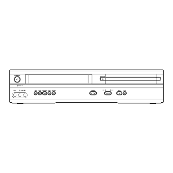
Page 12: Operating Controls And Functions
OPERATING CONTROLS AND FUNCTIONS 1-6-1 H9923IB... - Page 13 1-6-2 H9923IB...
-
Page 14: Signal Name Abbreviations
SIGNAL NAME ABBREVIATIONS Signal Name Function Signal Name Function Capstan Motor Rotation Detection C-FG FIP Drive Power Supply Pulse A-COM Audio Head Common Color Phase Rotary Changeover C-ROTA SIgnal AUDIO-IN Audio Signal Input C-SYNC Composite Synchronized Pulse AUDIO(L)-IN Audio(L) Signal Input CLKSEL Clock Select (GND) AUDIO(L)-IN-F Audio(L) Signal Input (Front) - Page 15 Signal Name Function Signal Name Function EV+11V +11V Power Supply P-ON-H Power On Signal at High EV+3.3V +3.3V Power Supply P61/LP P61/LP Filament Power Supply 1 P80/C P80/C Terminal Filament Power Supply 2 Video Head Switching Pulse PG-DELAY Signal Adjusted Voltage FE-H Full Erase Head POW-SAF...
- Page 16 Signal Name Function Component Video (Luminance) VIDEO-Y(I) Signal (Interlace) Component Video (Luminance) VIDEO-Y(I/P) Signal (Interlace/Progressive) XCin Sub Clock XCOUT Sub Clock Main Clock Input Xout Main Clock Input 1-7-3 H9923SNA...
-
Page 17: Cabinet Disassembly Instructions
CABINET DISASSEMBLY INSTRUCTIONS 1. Disassembly Flowchart REMOVAL This flowchart indicates the disassembly steps to gain REMOVE/*UNHOOK/ LOC. PART Fig. access to item(s) to be serviced. When reassembling, UNLOCK/RELEASE/ Note follow the steps in reverse order. Bend, route, and UNPLUG/DESOLDER dress the cables as they were originally. [1] Top Case DVD Main 2(S-6), *CN201,... - Page 18 Reference Notes CAUTION 1: Locking Tabs (L-1) and (L-2) are fragile. Be careful not to break them. (S-1) (S-1) 1-1. Release three Locking Tabs (L-1). [1] Top Case 1-2. Release three Locking Tabs (L-2), then remove the Front Assembly. (S-1) CAUTION 2: Electrostatic breakdown of the laser diode in the optical system block may occur as a potential difference caused by electrostatic charge...
- Page 19 CN401 (S-8) (S-3) (S-7) CN601 (S-7) [4] DVD (S-8) (S-3) Mechanism Assembly (S-3) (S-5) (S-4) (S-9) (S-9) [6] Loader Holder [8] VCR [5] Partition Chassis Unit Plate Fig. D3 Fig. D5 (S-6) (S-6) [7] DVD Main CBA Unit CN301 CN201 DVD Mechanism Short the three short lands by soldering.
- Page 20 Cylinder FE Head Assembly ACE Head Assembly [9] Deck Assembly [13] Jack Cover SW507 [14] Earth LD-SW [15] Jack Board Plate (S-12) (S-13) [11] Power SW CBA [12] Main CBA [9] Deck Assembly Cam Gear (S-10) [12] Main CBA Hole Shaft (S-11) Desolder...
- Page 21 HOW TO EJECT MANUALLY 1. Remove the Top Case, Front Assembly and Top Bracket. 2. Remove four Screws (S-3) in Fig. D3. Do not disconnect connectors. 3. While lifting up the DVD Mechanism, rotate the roulette in the direction of the arrow as shown below.
-
Page 22: Electrical Adjustment Instructions
ELECTRICAL ADJUSTMENT INSTRUCTIONS General Note: "CBA" is an abbreviation for "Circuit Board Assembly." NOTE: Figure 1 1.Electrical adjustments are required after replacing circuit components and certain mechanical parts. It is important to do these adjustments only after all repairs and replacements have been com- EXT. -
Page 23: How To Initialize The Dvd Player & Vcr
HOW TO INITIALIZE THE DVD PLAYER & VCR To put the program back at the factory-default, initialize the DVD player & VCR as the following procedure. < DVD Section > 1. Press [DVD], [1], [2], [3], [4], and [DISPLAY/ STATUS] buttons on the remote control unit in that order. -
Page 24: Firmware Renewal Mode
FIRMWARE RENEWAL MODE 1. Turn the power on and remove the disc on the tray. 5. After programming is finished, the tray opens automatically. Fig. e appears on the screen and 2. To put the DVD player into version up mode, press the checksum in (*2) of Fig. - Page 25 10. Press [CLEAR/C-RESET] button on the remote control unit. Fig. h appears on the screen. " ******* " differ depending on the models. MODEL : ******* Version : *.** Region : * EEPROM CLEAR : OK EEPROM CLEAR : CLEAR EXIT: POWER Fig.
-
Page 26: Block Diagrams
BLOCK DIAGRAMS <VCR SECTION> Servo / System Control Block Diagram H9923BLS 1-12-1... - Page 27 Video Block Diagram H9923BLV 1-12-2...
- Page 28 Audio Block Diagram H9923BLA 1-12-3...
- Page 29 Hi-Fi Audio Block Diagram H9923BLH 1-12-4...
- Page 30 Power Supply Block Diagram H9923BLP 1-12-5...
- Page 31 BLOCK DIAGRAMS <DVD SECTION> DVD System Control / Servo Block Diagram H9923BLSD 1-12-6...
- Page 32 Digital Signal Process Block Diagram H9923BLD 1-12-7...
- Page 33 DVD Video / Audio Block Diagram 1-12-8 H9923BLVD...
-
Page 34: Schematic Diagrams / Cba's And Test Points
SCHEMATIC DIAGRAMS / CBA'S AND TEST POINTS Standard Notes Notes: WARNING 1. Do not use the part number shown on these draw- ings for ordering. The correct part number is Many electrical and mechanical parts in this chassis shown in the parts list, and may be slightly different have special characteristics. - Page 35 Main 1/8 Schematic Diagram Parts Location Guide < VCR Section > Ref No. Position Ref No. Position CAPACITORS COILS C503 L503 TRANSISTORS C505 C506 Q506 C507 Q515 RESISTORS C508 C509 R513 C510 R517 C511 R536 C512 R537 C514 R538 C515 R539 C516 R540...
- Page 36 Main 1/8 Schematic Diagram < VCR Section > IC501 KEY VOLTAGE CHART Pin No. KEY 1 (7 PIN) KEY 2 (8 PIN) “ “ = SMD Voltage indications for PLAY, REC and DVD modes Voltage on the Schematic Diagrams are as shown below: 0.00 ~ 0.51V REC/OTR --------------...
- Page 37 Main 2/8, Sensor & Power SW Schematic Diagram < VCR Section > IC611 MATRIX CHART Voltage indications for PLAY, REC and DVD modes “ “ = SMD on the Schematic Diagrams are as shown below: SACD REPEAT PSCAN PLAY mode REC mode (2.5) DVD mode...
- Page 38 Main 2/8 Schematic Diagram Parts Location Guide < VCR Section > Ref No. Position Ref No. Position CAPACITORS RESISTORS C502 R527 C612 R528 C614 R530 C615 R532 C701 R601 C702 R602 C704 R603 C705 R604 C706 R605 C711 R611 C714 R612 C716 R613...
- Page 39 Main 3/8 Schematic Diagram Parts Location Guide < VCR Section > Ref No. Position Ref No. Position Ref No. Position Ref No. Position CAPACITORS CAPACITORS COILS RESISTORS C253 C345 L304 R323 C255 C346 L306 R325 C256 C348 L308 R327 C301 C349 L401 R328...
- Page 40 Main 3/8 Schematic Diagram < VCR Section > “ “ = SMD Voltage indications for PLAY, REC and DVD modes on the Schematic Diagrams are as shown below: PLAY mode REC mode (2.5) DVD mode < > The same voltage for Indicates that the voltage PLAY, REC &...
- Page 41 Main 4/8 Schematic Diagram < VCR Section > “ “ = SMD Voltage indications for PLAY, REC and DVD modes on the Schematic Diagrams are as shown below: PLAY mode REC mode (2.5) DVD mode < > The same voltage for Indicates that the voltage PLAY, REC &...
- Page 42 Main 5/8 Schematic Diagram < VCR Section > “ “ = SMD Voltage indications for PLAY, REC and DVD modes on the Schematic Diagrams are as shown below: PLAY mode REC mode (2.5) DVD mode < > The same voltage for Indicates that the voltage PLAY, REC &...
- Page 43 Main 6/8 & DVD Open/CloseSchematic Diagram < VCR Section > “ “ = SMD Voltage indications for PLAY, REC and DVD modes on the Schematic Diagrams are as shown below: PLAY mode REC mode (2.5) DVD mode < > The same voltage for Indicates that the voltage PLAY, REC &...
- Page 44 Main 6/8 Schematic Diagram Parts Location Guide < VCR Section > Ref No. Position Ref No. Position CAPACITORS RESISTORS C057 AH-3 R053 AH-4 C058 AH-3 R054 AI-4 C059 AH-3 R055 AH-4 C062 AH-3 R058 AI-4 C063 AG-3 R059 AI-4 C1039 AF-3 R060 AI-3...
- Page 45 Main 7/8 Schematic Diagram Parts Location Guide < VCR Section > Ref No. Position Ref No. Position CAPACITORS COILS C013 AN-4 L1001 AK-4 C014 AN-4 L1002 AK-3 C015 AN-4 L1003 AL-4 C017 AN-3 L1004 AM-3 C018 AN-3 L1005 AK-3 C019 AN-3 L1009 AN-2...
- Page 46 Main 7/8 Schematic Diagram < VCR Section > CAUTION ! CAUTION ! “ “ = SMD Voltage indications for PLAY, REC and DVD modes For continued protection against fire hazard, on the Schematic Diagrams are as shown below: Fixed voltage (or Auto voltage selectable) power supply circuit is used in this unit. replace only with the same type fuse.
- Page 47 Main 8/8 Schematic Diagram < VCR Section > “ “ = SMD Voltage indications for PLAY, REC and DVD modes on the Schematic Diagrams are as shown below: PLAY mode REC mode (2.5) DVD mode < > The same voltage for Indicates that the voltage PLAY, REC &...
- Page 48 Main CBA Top View CAUTION ! NOTE: For continued protection against fire hazard, The voltage for parts in hot circuit is measured using Sensor CBA Top View replace only with the same type fuse. hot GND as a common terminal. Because a hot chassis ground is present in the power CAUTION ! supply circut, an isolation transformer must be used.
- Page 49 Main CBA Bottom View < VCR Section > Because a hot chassis ground is present in the power CAUTION ! CAUTION ! supply circut, an isolation transformer must be used. For continued protection against fire hazard, Fixed voltage (or Auto voltage selectable) power supply circuit is used in this unit. Also, in order to have the ability to increase the input replace only with the same type fuse.
- Page 50 Main CBA Parts Location Guide Ref No. Position Ref No. Position Ref No. Position Ref No. Position Ref No. Position Ref No. Position Ref No. Position Ref No. Position Ref No. Position Ref No. Position Ref No. Position CAPACITORS CAPACITORS CAPACITORS CAPACITORS DIODES...
- Page 51 Power SW CBA Top View Power SW CBA Bottom View BH99A0F01011B DVD Open /Close DVD Open/Close CBA Bottom View CBA Top View BH99A0F01011C 1-13-18...
- Page 52 AFV Schematic Diagram AFV Schematic Diagram Parts Location Guide Ref No. Position Ref No. Position CAPACITORS CONNECTOR DIODE COILS RESISTORS CRYSTAL OSCILLATOR H9923SCAFV AFV CBA Bottom View AFV CBA Top View AFV CBA Parts Location Guide Ref No. Position Ref No. Position CAPACITORS CONNECTOR...
- Page 53 DVD Main 1/3 Schematic Diagram < DVD Section > 1 NOTE: Voltage indications for PLAY and STOP modes “ “ = SMD on the Schematic Diagrams are as shown below: Either IC461 or IC462 is used for DVD MAIN CBA UNIT. PLAY mode STOP mode (2.5)
- Page 54 DVD Main 2/3 Schematic Diagram < DVD Section > “ “ = SMD Voltage indications for PLAY and STOP modes on the Schematic Diagrams are as shown below: PLAY mode STOP mode (2.5) The same voltage for Indicates that the voltage both PLAY &...
- Page 55 IC101 Voltage Chart ~ : Voltage is not consistent ----- : Not used Unit : Volts PIN.NO PLAY STOP PIN.NO PLAY STOP PIN.NO PLAY STOP PIN.NO PLAY STOP PIN.NO PLAY STOP PIN.NO PLAY STOP PIN.NO PLAY STOP PIN.NO PLAY STOP ----- ----- -----...
- Page 56 DVD Main 3/3 Schematic Diagram < DVD Section > “ “ = SMD Voltage indications for PLAY and STOP modes on the Schematic Diagrams are as shown below: PLAY mode STOP mode (2.5) The same voltage for Indicates that the voltage both PLAY &...
-
Page 57: Waveforms
WAVEFORMS NOTE: Input VCR: COLOR BAR SIGNAL (WITH 1KHz AUDIO SIGNAL) (WF1~WF3) DVD: POWER ON (STOP) MODE (WF4~WF6) CD: 1kHz PLAY (WF7~WF9) TP301 UPPER TP504 Pin 8 of CN1601 Pin 13 of CN1601 LOWER C-PB AUDIO-L 0.5ms RF-SW 0.2V VIDEO-Y 0.2V 20µs TP751... -
Page 58: Wiring Diagram < Vcr Section
WIRING DIAGRAM < VCR SECTION > 1-15-1 H9923WI... -
Page 59: Wiring Diagram < Dvd Section
WIRING DIAGRAM < DVD SECTION > 1-15-2 H9923WID... -
Page 60: System Control Timing Charts
SYSTEM CONTROL TIMING CHARTS < VCR Section > Mode SW : LD-SW LD-SW Position detection A/D Input voltage Limit Symbol (Calculated voltage) 3.76V~4.50V (4.12V) 4.51V~5.00V (5.00V) 0.00V~0.25V (0.00V) 1.06V~1.50V (1.21V) 0.66V~1.05V (0.91V) 1.99V~2.60V (2.17V) 1.51V~1.98V (1.80V) 3.20V~3.75V (3.40V) 0.26V~0.65V (0.44V) 4.51V~5.00V (5.00V) 2.61V~3.19V... - Page 61 Still/Slow Control Frame Advance Timing Chart 1) SP Mode 18 RF-SW The first rise of RF-SW after a rise in F-AD signal F-AD (Internal Signal) "H" "H" "Z" C-DRIVE "L" "L" Stop detection (T2) Acceleration Detection (T1) Slow Tracking Value PB CTL Reversal Limit Value 20ms...
- Page 62 2) LP/SLP Mode 18 RF-SW The first rise of RF-SW after a rise in F-AD signal F-AD (Internal Signal) "H" "H" "Z" C-DRIVE "L" "L" Stop detection (T2) Acceleration Detection (T1) Slow Tracking Value PB CTL Reversal Limit Value 20ms 78 C-F/R 16 H-A-SW 15 C-ROTA...
- Page 63 EJECT ST-S/ END-S "OFF" CASS.LOAD LD-FWD 0.2S LD-REV 0.7S LD-FWD 0.4S LD-FWD 0.2S LD-REV 0.2S LD-FWD 0.5S LD-REV STOP(A) PLAY LD-FWD PLAY LD-FWD LD-REV 0.2S LD-FWD PLAY PLAY PAUSE (SLOW) LD-FWD STILL(SLOW) PLAY LD-REV 0.2S LD-FWD PLAY STOP /EJECT LD-REV STOP(A) Fig.
- Page 64 STOP(A) STOP LD-REV 0.2S LD-FWD STOP /EJECT 1.0S LD-FWD 0.5S LD-REV STOP(A) LD-REV 0.2S LD-FWD STOP /EJECT LD-REV 1.0S LD-FWD 0.5S LD-REV STOP(A) LD-FWD PAUSE LD-FWD 2.5S Short REV LD-REV 0.2S LD-FWD REC PAUSE REC or PAUSE STOP /EJECT LD-FWD 1.5S LD-REV 0.2S...
- Page 65 < DVD Section > Tray Close ~ Play / Play ~ Tray Open Tray Disc Disc Tray Play Close Rotation Stop Open 3.3V Tray IN (TL221) 1.65V Sled Drive (TP303) 1.65V Disc Drive (TP301) 1.65V Focus Drive (TP304) Tracking Drive 1.65V (TP302) 1-16-6...
-
Page 66: Ic Pin Function Descriptions
IC PIN FUNCTION DESCRIPTIONS < VCR Section > Signal Active Function Name Level IC501( SERVO / SYSTEM CONTROL IC ) POWER- “POWER” LED 23 OUT Signal Output “H” ≥ 4.5V, “L” ≤ 1.0V POWER- “POWER” LED 24 OUT Signal Active Signal Output Function Name... - Page 67 Signal Active Signal Active Function Function Name Level Name Level LPF Connected 83 OUT AUDIO- Audio Mute Control Terminal (Slicer) MUTE-H Signal (Mute = “H”) Not Used Not Used Not Used Not Used Not Used Hi-Fi Tape A-MODE Detection Signal Composite PULSE C-SYNC...
- Page 68 IC612 ( FIP DRIVER ) Signal Name Function Name FP-CLK Clock Input FP-STB Serial Interface Strobe Not Used Not Used Power Supply Segment Output Pull Down Level Segment Output Grid Output Power Supply Oscillator Input Not Used FP-DIN Serial Data Input 1-17-3 H9923PIN...
-
Page 69: Lead Identifications
LEAD IDENTIFICATIONS 2SA1175(F,H,J) 2SA1015-GR(TPE2) 2SC3266-Y(TPE2 F) MID-32A22F 2SC2785(F,H,J) 2SA1015-GR(TE2 F T) 2SC3266-Y(TPE2) PT204-6B-12 BA1F4M-T 2SC1815-BL(TPE2) KTC3203(Y) BN1F4M-T 2SC1815-GR(TPE2) KTC3203-Y-AT/P KRA103M 2SC1815-BL(TE2 F T) KTC3205(Y) KRC103M 2SC1815-GR(TE2 F T) KTC3205-Y-AT/P KRC103M-AT/P 2SC1815-Y(TE2 F T) KTA1266(GR) 2SC1815-Y(TPE2) KTA1267(GR,Y) 2SC2120-Y(TPE2) KTC3199(BL,GR,Y) 2SC2120-Y(TE2 F T) KTA1267-GR-AT/P KTA1267Y-AT/P KTC3199-(BL,GR,Y)-AT/P... -
Page 70: Electrical Parts List
1-19-1 ELECTRICAL PARTS LIST MISCELLANEOUS SW604 * 4822 276 14127 SKQSAF001A 9965 000 29469 DVD MAIN CBA UNIT 9965 000 29470 MCV CBA SW604 * 9965 000 19590 TACT SWITCH TC-1104(H=9.5) SW605 4822 276 13954 KSM0614B 9965 000 29471 AFV CBA 9965 000 24118 SENSOR CBA SW605 * 4822 276 14127... - Page 71 1-19-2 ELECTRICAL PARTS LIST COILS L010 * 9965 000 05627 CHOKE COIL 47UH-K L1521 * 9965 000 23990 CHOKE COIL 47UH-K L010 * 9965 000 05702 CHOKE COIL 47UH-K L1521 * 9965 000 27579 FIXED INDUCTORS LGB0810T-470K L010 * 9965 000 23990 CHOKE COIL 47UH-K L2001 4822 157 10649...
- Page 72 1-19-3 ELECTRICAL PARTS LIST DIODES D1018 * 4822 130 32778 1SS133 Q057 * 9965 000 10994 2SC3199-GR/KTC3199-GR D1019 9965 000 14881 ZENER DIODE DZ-6.8BSBT265 Q057 * 9965 000 09882 TRANSISTOR BN1L4M-T D1019 * 9965 000 23556 ZENER DIODE MTZJT-776.8B Q058 9965 000 29490 TRANSISTOR KTA1267Y-AT/P D1022...
- Page 73 1-19-4 ELECTRICAL PARTS LIST TRANSISTORS Q770 * 9965 000 29485 TRANSISTOR KTC3199-GR-AT/P Q1053 * 4822 130 63144 2SA1267(YG) Q770 * 4822 130 41306 2SC1815GR Q1053 * 4822 130 10462 KTA1267-GR Q770 * 9965 000 29486 TRANSISTOR 2SC1815-Y(TE2 F T) Q1054 9965 000 29484 TRANSISTOR KTC3199-Y-AT/P Q770 *...
- Page 74 1-19-5 ELECTRICAL PARTS LIST INTEGRATED CIRCUITS AFV CBA IC612 * 9965 000 27577 VFD DRIVER IC SC16313G 4822 130 30621 1N4148 IC751 9965 000 29478 IC SWITCH TC4053BF(EL N F) D2 * 4822 130 32778 1SS133 IC751 * 9965 000 13852 IC:SWITCH TC4053BF(N) OR 9965 000 14760 AUD UP MSP3417G-QG-B8-V3...
-
Page 75: Exploded Views
EXPLODED VIEWS Cabinet 2L071 2B21 2L071 2L071 2L021 2L071 2L021 2L023 2L021 L0-9 L0-9 2B20 2L082 2B18 2L023 2L062 2L023 JW002 2L021 Sensor CBA DVD Main CBA Unit AFV CBA 2B11 Power SW CBA Sensor CBA 2L051 The FFC calbes are included in 2B13 1B2 (DVD mechanism). - Page 76 Packing Unit Some Ref. Numbers are not in sequence. 1-20-2 H9923PEX...
- Page 77 1-21-1 MECHANICAL & ACCESSORY PARTS LIST ELECTRICAL PARTS 9965 000 29469 DVD MAIN CBA UNIT 9965 000 29470 MCV CBA(MAIN P_SW O_C SEN CBA) 9965 000 29471 AFV CBA 9965 000 24118 SENSOR CBA MECHANICAL PARTS 9965 000 29468 DECK ASSEMBLY CZD014/VM2560 9965 000 27556 DVD MECHA E6160(FG LESS) 9965 000 29466...
Need help?
Do you have a question about the DVP3050V/75 and is the answer not in the manual?
Questions and answers