Table of Contents
Advertisement
Quick Links
Download this manual
See also:
User Manual
DVD Home Theater System
Service
Service
Service
Service Manual
Copyright 2010 Philips Consumer Electronics B.V. Eindhoven, The Netherlands
©
All rights reserved. No part of this publication may be reproduced, stored in a retrieval system or
transmitted, in any form or by any means, electronic, mechanical, photocopying, or otherwise
without the prior permission of Philips.
Published by
RY1014
Service Audio Printed in The Netherlands Subject to modification
Version 1.1
TABLE OF CONTENTS
Location of PCB Boards ............................................ 1-2
Versions Variation ...................................................... 1-2
Specifications ............................................................ 1-3
Measurement Setup .................................................. 1-4
Service Aids .............................................................. 1-5
ESD & Safety Instruction .......................................... 1-6
Lead-free soldering Information ................................ 1-7
Setting procedure & Repair Instructions........................ 2
Disassembly Instructions & Service positions .............. 3
Block & Wiring Diagram ................................................ 4
VFD+USB+AUX Board .................................................. 5
Main+LED Board............................................................ 6
Power Board .................................................................. 7
AMP Board .................................................................... 8
Touch Board .................................................................. 9
Mechanical Exploded view .......................................... 10
Revision List ................................................................ 11
1 - 1
Chapter
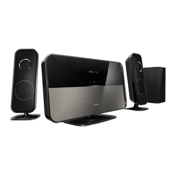
HTS5200
/12/98/51
GB
3139 785 35301
Advertisement
Table of Contents

Related Manuals for Philips HTS5200/12


Summary of Contents for Philips HTS5200/12
- Page 1 Touch Board ..............9 Mechanical Exploded view .......... 10 Revision List ..............11 Copyright 2010 Philips Consumer Electronics B.V. Eindhoven, The Netherlands © All rights reserved. No part of this publication may be reproduced, stored in a retrieval system or transmitted, in any form or by any means, electronic, mechanical, photocopying, or otherwise without the prior permission of Philips.
-
Page 2: Location Of Pcb Boards
1 - 2 LOCATION OF PCB BOARDS POWER PCB MAIN PCB TOUCH PCB VFD PCB LED PCB AUX PCB POWER PCB USB PCB DOOR LED PCB TOP VIEW BOTTOM VIEW VERSION VARIATION: Type/Versions HTS5200 Features Output Power - 400W Voltage (110~127V) Voltage (220~240V) REPAIR SCENARIO MATRIX: HTS5200... -
Page 3: Specifications
1 - 3 SPECIFICATIONS Playback media Main Unit DVD-Video, DVD+R/+RW, DVD-R/-RW, DVD+R DL,CD-R/CD- Power supply ................RW, Audio CD, Video CD/SVCD, Picture CD, MP3-CD, WMA- Russia/China/India ........220-240V; ~50 Hz CD, DivX-CD, USB storage device (for /12/98) Asia Pacifi c/Latin America ............AVCHD, BD-RE, BD-Video, DVD-Video, DVD+R/+RW, DVD- ........110-127V/220-240V;... - Page 4 1 - 4 MEASUREMENT SETUP Tuner FM Bandpass LF Voltmeter 250Hz-15kHz e.g. PM2534 e.g. 7122 707 48001 RF Generator e.g. PM5326 S/N and distortion meter e.g. Sound Technology ST1700B Use a bandpass filter to eliminate hum (50Hz, 100Hz) and disturbance from the pilottone (19kHz, 38kHz). Use Audio Signal Disc SBC429 4822 397 30184 (replaces test disc 3)
- Page 5 1 - 5 SERVICE AIDS Service Tools: Universal Torx driver holder .........4822 395 91019 Torx bit T10 150mm ...........4822 395 50456 Torx driver set T6-T20 .........4822 395 50145 Torx driver T10 extended ........4822 395 50423 Compact Disc: SBC426/426A Test disc 5 + 5A ......4822 397 30096 SBC442 Audio Burn-in test disc 1kHz ....4822 397 30155 SBC429 Audio Signals disc .........4822 397 30184 Dolby Pro-logic Test Disc ........4822 395 10216...
- Page 6 1 - 6 WAARSCHUWING WARNING Alle IC’s en vele andere halfgeleiders zijn All ICs and many other semi-conductors are gevoelig voor electrostatische ontladingen susceptible to electrostatic discharges (ESD). (ESD). Careless handling during repair can reduce life Onzorgvuldig behandelen tijdens reparatie kan drastically.
- Page 7 You will find this and more technical information • Use only lead-free solder alloy Philips SAC305 with within the “magazine”, chapter “workshop news”. order code 0622 149 00106. If lead-free solder-paste is required, please contact the manufacturer of your For additional questions please contact your local solder-equipment.
- Page 8 2 - 1 2 - 1 c) Remove solder joint on the ESD protection point. System , Region Code , etc. Setting Produre 1)Restore factory setting 6) Upgrading new software a) Press <SETUP> button on R/C a) Copy the latest upgrading software onto a CD-R or USB storage b) Select <preference setup>...
- Page 9 2 - 2 2 - 2 REPAIR INSTRUCTIONS (One)
- Page 10 2 - 3 2 - 3 REPAIR INSTRUCTIONS (Two)
- Page 11 2 - 4 2 - 4 REPAIR INSTRUCTIONS (Three)
- Page 12 3 - 1 3 - 1 DISASSEMBLY INSTRUCTIONS Dismantling of Rear Panel Dismantling of the Main PCB 1) Using hands to push the cable door to remove it as shown in fi gure 1. 1) Loosen 8 screws “C” to remove main PCB bracket as shown in fi gure 4. 2) Loosen 2 screws “A”...
- Page 13 3 - 2 3 - 2 Dismantling of the USB+AUX PCB 1) Loosen 2 screws “F” at the main PCB bracket to remove AUX PCB as shown in fi gure 7. 2) Loosen 9 screws “G” to remove DVD fan bracket&fan&USB bracket as shown in fi gure 8. 3) Loosen 2 screws “H”...
-
Page 14: Service Positions
3 - 3 3 - 3 Dismantling of the DVD Module SERVICE POSITIONS 1) Loosen 3 screws “L” at the power PCB bracket bottom to remove DVD module as shown in fi gure 13. Figure 13 Dismantling of the VFD+LED+DVD LED PCB 1) Loosen 3 screws “M”... - Page 15 4 - 1 4 - 1 BLOCK DIAGRAM...
- Page 16 4 - 2 4 - 2 WIRING DIAGRAM...
-
Page 17: Vfd+Usb+Aux Board
5 - 1 5 - 1 FTD DISPLAY PIN ASSIGNMENT VFD+USB+AUX BOARD TABLE OF CONTENTS FTD Display Pin Assignment ............. 5-1 Circuit Diagram ................. 5-2 PCB Layout Top & Bottom View ............5-3 PIN CONNECTION... - Page 18 5 - 2 5 - 2 CIRCUIT DIAGRAM C300 C502 C507 C513 C518 C523 C528 FB300 JK300 Q504 R504 R510 R515 R521 R526 R533 RB301 A1 USB300 A1 C302 C503 C508 C514 C519 C524 FB301 LD502 R500 R505 R511 R516 R522 R527 R534...
- Page 19 5 - 3 5 - 3 PCB LAYOUT - TOP VIEW C502 C504 C520 DP500 A2 J501 J503 J505 JK300 Q501 R507 R534 RB300 B2 RB503 B1 RB507 A1 USB300 B2 C503 C519 C521 J500 J502 J504 J506 LD502 Q503 R510 RB301 B2 RB506 A1...
-
Page 20: Main+Led Board
6 - 1 6 - 1 INTERNAL IC DIAGRAM - MT1389FEX/SN DVB-T HDMI1.2Tx RGB video Module MT1389S CVBS MAIN+LED BOARD FLASH 8ch Audio SPDIF Front-panel USB2.0/3 in 1 card DRAM Remote reader TABLE OF CONTENTS Internal IC Diagram ................6-1 Circuit Diagram(part one) .............. - Page 21 6 - 2 6 - 2 CIRCUIT DIAGRAM - part one C0201 C2 C0216 D1 C0239 D4 C0601 C4 C211 D4 C231 D2 C601 C4 C721 A3 C807 B1 C824 B2 C839 B2 C859 C1 CE218 C2 CN306 A4 FB205 C4 FB308 A4 FB803 B1 JK701 A3...
- Page 22 6 - 3 6 - 3 CIRCUIT DIAGRAM - part two C303 A2 C313 A2 C327 A2 C342 A2 C352 B1 C366 A1 C395 C2 C742 A2 C904 C1 C921 C1 CE305 C1 CE321 C2 CE345 A1 CN303 B1 FB315 B3 FE307 C2 IC306 B3 R3020 B2...
- Page 23 6 - 4 6 - 4 PCB LAYOUT - TOP VIEW C0202 A3 C214 B3 C261 B1 C341 B2 C367 A1 C718 A2 C746 A1 C823 B3 C849 B2 C924 A1 CN301 B2 FB201 B3 FB308 B1 FB801 C2 IC302 A1 L207 B2 Q307 C1 Q805 B2...
- Page 24 6 - 5 6 - 5 PCB LAYOUT - BOTTOM VIEW C0201 B3 C0210 A2 C0218 B3 C0227 B3 C0239 A3 C0245 B2 C0253 A2 C0606 A3 C227 B2 C306 A1 C324 B1 C518 C1 C802 C2 C836 B2 C864 A3 CE201 C2 CE212 B1 CE306 A1...
-
Page 25: Power Board
7 - 1 7 - 1 INTERNAL IC DIAGRAM - AZ431 CATHODE POWER BOARD ANODE TABLE OF CONTENTS Internal IC Diagram ................7-1 Circuit Diagram .................. 7-2 PCB Layout Top View ............... 7-3 PCB Layout Bottom View ..............7-4 INTERNAL IC DIAGRAM - AZ7500BP OUTPUT CTRL Oscillator Pulse-Steering... - Page 26 7 - 2 7 - 2 CIRCUIT DIAGRAM BD901 A1 C919 B1 C929 B2 C946 A2 C956 C2 C967 B2 C977 B1 C993 B3 D904 B2 D915 A3 F901 C1 L904 B2 Q906 B3 Q917 C3 R908 A1 R920 C2 R930 C2 R942 B1 R955 C2...
- Page 27 7 - 3 7 - 3 PCB LAYOUT - TOP VIEW BD901 B1 C918 C923 C960 C966 C973 C982 CN904 A3 D907 D922 F901 J902 J907 J912 J917 L904 NTC901 A1 Q910 R912 R940 R949 R981 T903 C901 C919 C926 C961 C968 C974...
- Page 28 7 - 4 7 - 4 PCB LAYOUT - BOTTOM VIEW C903 A1 C927 A3 C939 A3 C948 A3 C955 A3 C972 B3 C991 A3 D906 B2 D915 A3 Q902 A3 Q918 A3 R905 A1 R911 A3 R920 A2 R927 A2 R937 A2 R953 B3 R959 A3...
-
Page 29: Amp Board
8 - 1 8 - 1 INTERNAL IC DIAGRAM - TA5508APAG AMP BOARD TABLE OF CONTENTS Internal IC Diagram ................8-1 INTERNAL IC DIAGRAM - TAS5342ADDV Circuit Diagram .................. 8-2 PCB Layout Top View ............... 8-3 PCB Layout Bottom View ..............8-4... - Page 30 8 - 2 8 - 2 CIRCUIT DIAGRAM C600 A1 C611 A1 C622 A1 C632 A2 C649 B2 C660 C1 C671 C2 C682 A1 C701 C1 C713 C2 C724 C3 D604 B3 FB603 B1 L607 Q610 B3 R607 A2 R630 B1 R661 B1 R672 C2 R683 B2...
- Page 31 8 - 3 8 - 3 PCB LAYOUT - TOP VIEW C604 B3 C615 A2 C630 B3 C646 B3 C655 B2 C664 B2 C674 B2 C683 B1 C700 A1 C717 A1 C726 B1 D604 B1 IC601 A2 L608 B2 Q608 B1 R608 A2 R629 B2 R638 A2...
- Page 32 8 - 4 8 - 4 PCB LAYOUT - BOTTOM VIEW C600 A3 C602 B3 C608 A3 C621 B3 C624 B3 C627 B3 C629 B3 C669 B1 C706 B1 C709 B1 C711 B1 D607 B3 D609 B3 D701 B3 R601 B3 R605 B3 R700 B3 R712 B1...
-
Page 33: Touch Board
9 - 1 9 - 1 TOUCH BOARD TABLE OF CONTENTS Circuit Diagram .................. 9-2 PCB Layout Top View & Bottom View ..........9-3... - Page 34 9 - 2 9 - 2 CIRCUIT DIAGRAM C11 C2 C13 C2 CN1 C2 IC1 B1 R11 C1 R13 C1 R15 C2 R17 B2 R19 C2 R21 B2 C10 C2 C12 C2 CN2 A1 R10 C1 R12 C1 R14 C2 R16 B2 R18 C2 R20 B2...
- Page 35 9 - 3 9 - 3 PCB LAYOUT - TOP VIEW CN1 A1 CN2 A2 PCB LAYOUT - BOTTOM VIEW...
-
Page 36: Mechanical Exploded View
10 - 1 10 - 1 Mechanical Exploded View Door LED PCB VIDEO SCART A1=21+24 A2=4+41+44+46 A3=30+31+38+27+29+28 A4=1+3+5... -
Page 37: Revision List
11 - 1 REVISION LIST Version 1.0 *Initial release Version 1.1 *Update chapter 1&2...
Need help?
Do you have a question about the HTS5200/12 and is the answer not in the manual?
Questions and answers