Advertisement
Quick Links
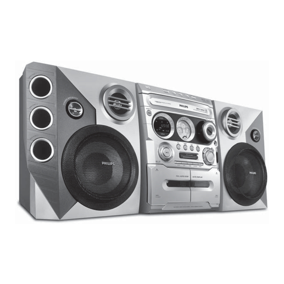
DVD Micro Theatre
©
Copyright 2006 Philips Consumer Electronics B.V. Eindhoven, The Netherlands
All rights reserved. No part of this publication may be reproduced, stored in a retrieval system or
transmitted, in any form or by any means, electronic, mechanical, photocopying, or otherwise without
the prior permission of Philips.
Published by SL 0617 Service Audio
Version 1.0
TABLE OF CONTENTS
Location of PC Boards & Versions Variation ........................ 1-2
Specifi cations ....................................................................... 1-3
Measurement Setup ............................................................. 1-4
Service Aids, Safety Instruction, etc ...........................1-5 to 1-7
Connections & Functional Overview......................... 1-8 to 1-11
Troubleshooting ......................................................1-12 to 1-13
Repair Instructions................................................................... 2
Disassembly Instructions & Service positions ......................... 3
Set Block Diagram ................................................................ 4-1
Set Wiring Diagram .............................................................. 4-2
Control Board .......................................................................... 5
Main Board .............................................................................. 6
Tuner Board ............................................................................. 7
Power Board ............................................................................ 8
Mechanical Exploded View & Parts List .................................. 9
Printed in The Netherlands
Subject to modification
FWD573
Page
CLASS 1
LASER PRODUCT
© 3141 785 30790
/55/98
VIDEO CD
Advertisement

Related Manuals for Philips FWD573/55


Summary of Contents for Philips FWD573/55
- Page 1 LASER PRODUCT © Copyright 2006 Philips Consumer Electronics B.V. Eindhoven, The Netherlands All rights reserved. No part of this publication may be reproduced, stored in a retrieval system or transmitted, in any form or by any means, electronic, mechanical, photocopying, or otherwise without the prior permission of Philips.
- Page 2 LOCATION OF PC BOARDS MAIN PCB TUNER PCB CONTROL PCB POWER PCB MICPHONE PCB VERSION VARIATION: Type /Versions FWD573 Features&Board in used P-scan Divx Main board Power board Tuner board Control board...
-
Page 3: Specifications
Specifications MAIN UNIT AMPLIFIER SECTION Power Supply Rating ......110 - 127 / 220 - 240 V Output power ..........3300 W PMPO .............. 50/60HZ Switchable Stereo mode ............ 2x125 W RMS Power Consumption Frequency Response ....... 150 Hz - 18 kHz / ± 3 dB Active ................ -
Page 4: Measurement Setup
MEASUREMENT SETUP Tuner FM Bandpass LF Voltmeter 250Hz-15kHz e.g. PM2534 e.g. 7122 707 48001 RF Generator e.g. PM5326 S/N and distortion meter e.g. Sound Technology ST1700B Use a bandpass filter to eliminate hum (50Hz, 100Hz) and disturbance from the pilottone (19kHz, 38kHz). Tuner AM (MW,LW) Bandpass LF Voltmeter... - Page 5 SERVICE AIDS Service Tools: ESD Equipment: Universal Torx driver holder ........4822 395 91019 Anti-static table mat - large 1200x650x1.25mm ... 4822 466 10953 Torx bit T10 150mm ..........4822 395 50456 Anti-static table mat - small 600x650x1.25mm ..4822 466 10958 Torx driver set T6 - T20 .........
- Page 6 WAARSCHUWING WARNING Alle IC’s en vele andere halfgeleiders zijn All ICs and many other semi-conductors are gevoelig voor electrostatische ontladingen susceptible to electrostatic discharges (ESD). (ESD). Careless handling during repair can reduce life Onzorgvuldig behandelen tijdens reparatie kan drastically. de levensduur drastisch doen verminderen. When repairing, make sure that you are Zorg ervoor dat u tijdens reparatie via een connected with the same potential as the mass...
- Page 7 To avoid wear-out of tips switch off un-used equipment, or reduce heat. • Mix of lead-free solder alloy / parts with leaded solder alloy / parts is possible but PHILIPS recommends strongly to avoid mixed solder alloy types (leaded and lead-free).
- Page 8 1 - 8 CONNECTIONS...
- Page 9 1 - 9 CONNECTIONS...
- Page 10 1 - 10 CONNECTIONS...
- Page 11 1 - 11 FUNCTIONAL OVERVIEW...
- Page 12 1 - 12 FUNCTIONAL OVERVIEW...
- Page 13 1-13 TROUBLESHOOTING...
- Page 14 System, Region code, Tuner, etc. setting procedure 5. Video Out Change 3) Region code change timer reset a) Press "SYSTEM" on R/C button Press below key to reset the timer : Hence in total, reprograming will be done by way of the 1) System Reset b) Select the menu using the "...
- Page 17 DISMANTLING INSTRUCTIONS Dismantling the DVD Module Dismantling of the Cover Front Display 1) Remove the Volume knobs as stated in Dismantling the Cover Front Display in Figure 7. 1) Loosen the 4 screws at top cover , 2 screws at slide Cover and 4 screws at back panel as Figure 1 &...
- Page 18 Dismantling of the Control Board & Cassette Module Dismantling of the Power Board 1) Loosen 4 screws 'J' to remove the Power Board figure 13. 1) Loosen 8 screws 'H' to remove the control board figure 11. Figure 11 2) Loosen 4 screws 'I' to remove the Cassette Module figure 12. Figure 13 Figure 12...
-
Page 19: Service Positions
Service positions Service position A Service position B Note: After re-assembly, it is very important to ensure the wires are properly inserted into their respective sockets and routed not to touch or obstruct any moving parts. Service position C... - Page 20 BLOCK DIAGRAM Control system Tuner system...
- Page 21 WIRING DIAGRAM Loader Power Board RB202 CN810 JK203 CN151 CN801 CN301 JK202 Main Board RB203 CN251 JK201 JK301 CN910 CN911 JK401 Control board CN703 CN704 CN705 JK501 CN501 CN701 CN702 Tuner board Tape Deck...
- Page 22 FTD DISPLAY PIN ASSIGNMENT CONTROL BOARD TABLE OF CONTENTS FTD Display Pin Assignment ............... 5-1 Pin Connection ..................5-1 Circuit Diagram (Top left) ..............5-2 Circuit Diagram (Top right) ..............5-3 Circuit Diagram (Bottom left) ............5-4 Circuit Diagram (Bottom right) ............5-5 PCB Layout Top View ................
- Page 23 CIRCUIT DIAGRAM: CONTROL PCB (TOP LEFT) C1806 A8 C2008 G5 C2015 D1 C2023 F2 C2031 F2 C226 CN551 B8 D257 D266 JK3001 A1 LD265 C9 Q255 Q264 R2004 G2 R2011 G2 R2019 F4 C2001 G4 C2009 G5 C2016 D1 C2024 G4 C2032 C7 C227 D250...
- Page 24 CIRCUIT DIAGRAM: CONTROL PCB (TOP RIGHT) R2024 R2031 G1 R2040 D1 R2056 D3 R2076 R2087 R286 R293 RB251 F1 TA251 G4 TA262 TA270 TA278 XL251 G4 R2025 R2032 G2 R2041 D1 R2057 D3 R2078 R2088 R287 R294 RB252 A2 TA253 G4 TA263 C5 TA271 C5 TA279...
- Page 25 CIRCUIT DIAGRAM: CONTROL PCB (BOTTOM LEFT)
- Page 26 CIRCUIT DIAGRAM: CONTROL PCB (BOTTOM RIGHT)
- Page 27 PCB LAYOUT: CONTROL PCB (TOP VIEW) C4003 C5154 FB402 R5089 C4006 C5179 FB403 R5090 C4007 C5205 FB404 R5091 C4010 C5210 FB405 R5092 C4011 C5211 IC5002 B7 R5093 C4012 C5213 IC5003 C7 R5094 C4013 C5217 Q5009 R5095 C4014 C5218 Q5011 R5096 C4015 C5220 Q5013...
- Page 28 PCB LAYOUT: CONTROL PCB (BOTTOM VIEW) C2001 C3 C2005 C2 C2007 B2 C2011 B1 C2019 B4 C2024 C3 C2027 C1 C2030 B1 C2225 C3 C2227 C3 IC251 B1 Q259 C2 ZD251 B4 C2002 C3 C2006 B1 C2008 B1 C2015 B4 C2020 B4 C2025 C3 C2029 C3 C2031 C3 C2226 C3 C2228 C3 IC255 C4 R2014 C3 ZD252 B4...
- Page 29 PCB LAYOUT: CONTROL SW PCB Voltage IC251 C851 CN803A A3 CN806A B2 CN808A B2 J801 J803 J805 SW801 Pin NO C852 CN804A B1 CN807A B2 CN810A A3 J802 J804 J806 SW802 Voltage 0.00 4.84 0.00 4.85 4.64 4.60 0.00 4.91 4.70 0.00 0.00...
- Page 30 ELECTRICAL PARTS LIST - CONTROL BOARD ELECTRICAL PARTS LIST - KEY BOARD DP201 9940 000 00879 VFD 46X26MM HNA-11LS11T TA277 9940 000 00872 TACT SW 50MA 12V ESDZ1 9965 000 26930 CHIP ZENER 5.6V 0.05 0.5W TA278 9940 000 00872 TACT SW 50MA 12V TA280 9940 000 00872...
- Page 31 ES8380 PHOENIX INTERNAL IC DIAGRAM Motor DVD/CD Motor Driver MAIN BOARD Video TV Display Audio Speakers SDRAM Audio Microphone In ES8380 (8/16-MB) Phoenix S/P DIF A/V Receiver EEPROM VFD Panel VFD Driver ROM/Flash IR Remote TABLE OF CONTENTS INTERNAL IC DIAGRAM ............. 6-1 Voltage List ................
- Page 32 VOLTAGE IC201 IC501 Pin NO Pin NO Voltage 3.40 1.52 0.80 0.04 1.66 0.41 0.46 0.03 0.00 3.40 0.15 0.14 0.02 0.16 1.15 3.06 1.42 Voltage 0.00 0.00 0.00 -11.95 0.00 0.00 0.00 13.34 Pin NO Voltage 3.40 3.26 0.00 3.40 2.00 0.14...
- Page 33 CIRCUIT DIAGRAM -MAIN SERVO C0201 D3 C0225 B8 C0254 B1 C0283 B8 C2026 A2 C211 C238 C261 C287 C385 CN251 B1 FB212 B3 FB234 A8 IC305 D7 L251 R203 R226 R250 R273 R378 R814 R841 ZD209 D6 C0202 D3 C0226 B8 C0255 B1 C0284 B8 C2027 A1...
- Page 34 CIRCUIT DIAGRAM - MAIN AMPLIFIER(TOP LEFT)
- Page 35 CIRCUIT DIAGRAM - MAIN AMPLIFIER(TOP RIGHT)
- Page 36 CIRCUIT DIAGRAM -MAIN AMPLIFIER (BOTTOM LEFT)
- Page 37 CIRCUIT DIAGRAM -MAIN AMPLIFIER (BOTTOM RIGHT)
- Page 38 PCB LAYOUT: MAIN (TOP) VIEW C0232 C457 D3010 L211 R3021 R5004 C0250 C458 D3011 L213 R3022 R5005 C0258 C459 D3011 L214 R3023 R5006 C0259 C460 D3012 L215 R303 R5017 C0261 C461 D3013 L250 R3030 R509 C0262 C462 D3015 L251 R304 R510 C0270 C465...
- Page 39 PCB LAYOUT MAIN (BOTTOM) VIEW C0201 C273 FB213 R5207 C0202 C278 FB214 R5208 C0203 C279 FB233 R5209 C0204 C280 FB234 R521 C0205 C281 FB804 R5210 C0206 C282 IC207 R5211 C0207 C283 L202 R5220 C0208 C284 L203 R5225 C0209 C285 L205 R5226 C0210 C286...
- Page 40 6-10 6-10 ELECTRICAL PARTS LIST - MAIN BOARD ELECTRICAL PARTS LIST - MAIN BOARD IC101 9965 000 29611 IC 8P CO4558A SO8 CERAMATE Q3001 9940 000 00915 XISTR NPN 2SC1623 RA207 9940 000 05229 RES.ARRAY 100Ω 1/16W 5% IC201 9940 000 05336 IC 208P ES8380FCD PQFP Q3002 9940 000 00921...
- Page 41 TUNER ADJUSTMENT TABLE Waverange Input frequency Input Tuned to Adjust Output Scope/Voltmeter VARICAP ALIGNMENT 108MHz 7.5V 1V check 87.5 - 108MHz (50kHz grid) 87.5MHz check 1.4V 0.2V 1602KHz 7.2V 1V check T005 531KHz 1.1V 0.2V 531-1602kHz (9kHz grid) TUNER BOARD 530-1700kHz 1700KHz check...
- Page 42 CIRCUIT DIAGRAM : TUNER BOARD (/55 & /98 ver.) ANT001 C011 C022 C033 C043 D004 Q003 R016 R027 VC001 C002 C012 C023 C034 C044 D005 Q004 R017 R028 VC002 C004 C013 C024 C035 C047 IC001 R001 R018 R029 VD001 C005 C014 C025 C036...
- Page 43 PCB LAYOUT - TUNER BOARD (TOP VIEW) - /55 & /98ver. ANT001 A2 JMP4 C005 JMP5 C006 JMP6 C007 JMP7 C009 JMP8 JMP9 C019 L001 C024 C025 Q001 C030 Q002 C035 R018 C047 T001 CN001 T002 CN002 T003 D001 T005 D002 T006 D003...
- Page 44 VOLTAGE IC901 Pin NO Voltage 3.66 0.01 0.40 1.90 0.00 2.66 15.87 5.00 IC902 Pin NO Voltage 5.00 2.70 3.96 IC903 Pin NO Voltage 3.90 0.00 2.40 IC904 Pin NO Voltage 4.90 4.90 0.00 0.40 1.30 3.20 0.00 1.20 1.20 13.30 13.30 4.90...
- Page 45 CIRCUIT DIAGRAM-POWER BOARD BD901 D1 C914 C928 C942 C956 C971 D908 GT902 C1 L904 Q904 R901 R915 R929 R945 R960 R974 R989 C902 C915 C929 C943 C957 CN901 A1 D909 GT903 B1 L905 Q905 R902 R916 R931 R946 R961 R975 T901 C903 C916...
- Page 46 PCB LAYOUT-POWER BOARD BD901 A1 C914 C928 C942 C956 C971 D908 GT902 B1 J905 J920 L907 Q912 B3 R906 R920 R935 R949 R963 R977 T901 C901 C915 C929 C943 C957 CN901 B1 D909 GT903 B2 J906 J921 NTC901 B1 Q913 B3 R907 R921 R936...
- Page 47 ELECTRICAL PARTS LIST - POWER BOARD BD901 9965 000 28768 BRIDGE KBU8B 8A 100V L901 9940 000 05233 COMMON COIL 22MH C902 9940 000 05343 COND SAF. 0.22µF 275V 20% L902 9940 000 05233 COMMON COIL 22MH C903 9965 000 27115 CAP.
- Page 48 SET MECHANICAL EXPLODED VIEW...
- Page 49 MECHANICAL & ACCESSORIES PARTS LIST ELECTRICAL PARTS LIST - MISCELLANEOUS 9940 000 00824 FFC CABLE 9P P=1.27MM 80MM 9940 000 00825 FFC CABLE 12P P=1.27MM 100MM 9940 000 00919 FFC CABLE 24P P=0.5MM 380MM 9940 000 05353 FFC 9P 80MM P=1.27MM 9940 000 05354 FFC 12P 100MM P=1.27MM 9940 000 05356...
Need help?
Do you have a question about the FWD573/55 and is the answer not in the manual?
Questions and answers