
Subscribe to Our Youtube Channel
Summary of Contents for Lierda LSD4WF-2MD05101
- Page 1 Lierda Science & Technology Ltd LSD SCIENCE & TECHNOLOGY CO., LTD. LSD4WF-2MD05101 Low Power Wi-Fi Module User Manual FCC ID:N8NLSD4WF Model :LSD4WF-2MD05101 Name :Wi-Fi Module Revision :v1.0...
-
Page 2: Table Of Contents
Index 1. Product overview..............................3 1.1 General Description..........................3 1.2 Features................................3 2. Parameters................................4 3. Package.................................. 4 4. Pin definition.................................5 5. Behavior of electricity............................6 6. Typical application...............................7 7. Reference design..............................7 8. Developing tool..............................8... -
Page 3: Product Overview
1. Product overview 1.1 General Description LSD4WF-2MD05101 is a Wi-Fi module for any electronic device to achieve networking capabilities. The module is fully in line with the 802.11b/g/n international standard specification, the internal integrated high performance Cortex M4 and Wi-Fi chip make it easy to access the serial port equipment or MCU control equipment to network, so as to realize wireless networking. -
Page 4: Parameters
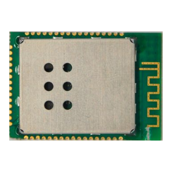
Security WEP/WPA-PSK/WPA2-PSK Mechanism Software Encryption WEP/AES/TKIP parameters Hardware Local wireless upgrading/ Web page upgrading upgrading/ Remote upgrading Network Protocol IPv4, TCP/UDP/FTP/HTTP User QJoine Configuration, AT+instruction, Web Configuration page Pic1-1 LSD4WF-2MD05101 Basic Parameters 3. Package Pic 1-2 LSD4WF-2MD05101 Front and back... -
Page 5: Pin Definition
Unit:mm Pic 1-3 LSD4WF-2MD05101 module package dimension 4. Pin definition Pic 1-4 LSD4WF-2MD05101 Module pin layout Pin definition Function... -
Page 6: Behavior Of Electricity
GPIO1/USART_CTS/TIM1_CH4/SPI4_MISO IOport/USARTport/timer/SPIport GPI04/ADC1_9/TIM3_CH4/nLink Multiplex pin:IOport/ADC/timer GPI05/ADC1_8/TIM3_CH3/nReady Multiplex pin:IOport/ADC/timer GPI06/ADC1_4/nReload Multiplex pin:IOport/ADC RST/nReset Reset pin Ground pin Table 1-1 LSD4WF-2MD05101 Module pin definition 5. Behavior of electricity Parameters Minimum Typical value Maximum Unit Working voltage Standby current Static current TX current... -
Page 7: Typical Application
Table 1-3 Connection introduction of cardinal pin 7. Reference design PCB onboard antenna is built in LSD4WF-2MD05101 module, users should using onboard antenna design need to be cautious that: 1, No components or GND on antenna area of user board 2, Keep antenna away from metal, stay over 10mm away from surrounding higher components. -
Page 8: Developing Tool
During specific design, users can consult the Lierda technical engineer to assist in the place of the module and related Layout. 8. Developing tool Lierda would provide a complete set of LSD4WF-2MD05101 development kit for customers to get familiar with the application and development of the module. Users can configure and debug the parameters of the LSD4WF-2MD05101 module through the USB interface and the function test. - Page 9 4Pin USB and RS232 debugging choosing port, left JMP3 choose USB 3Pin RS485 与 RS232 debugging choosing port, no JPM6 wire jumper choose RS232 EXT_PORT LSD4WF-2MD05101 GPIO interface expand JTAG JTAG data debugging interface Battery Lithium battery supply interface Power 3.3V power indication...
- Page 10 (OEM) Integrator has to assure compliance of the entire end‐product incl. the integrated RF Module. Additional measurements (15B) and/or equipment authorizations (e.g Verification) may need to be addressed depending on co‐location or simultaenous transmission issues if applicable. Integrator is reminded to assure that these installation instructions will not be made available to the end‐user of the final host device. With the low output power, this RF Module meets the FCC SAR exemption and can be therefore integrated into any (portable, mobile, fixed) host device. The final host device, into which this RF Module is integrated" has to be labelled with an auxilliary lable stating the FCC ID of the RF Module, such as "Contains FCC ID: ". N8NLSD4WF Depending on the size of the final end‐product, the §15.19 FCC statement "This device complies with part 15 of the FCC rules. Operation is subject to the following two conditions: (1) this device may not cause harmful interference, and (2) this device must accept any interference received, including interference that may cause undesired operation." ...
- Page 11 : This equipment has been tested and found to comply with the limits for a Class B digital device, pursuant to part 15 of the FCC Rules. These limits are designed to provide reasonable protection against harmful interference in a residential installation. This equipment generates, uses and can radiate radio frequency energy and, if not installed and used in accordance with the instructions, may cause harmful interference to radio communications.
Need help?
Do you have a question about the LSD4WF-2MD05101 and is the answer not in the manual?
Questions and answers