Table of Contents
Advertisement
Quick Links
SERVICE MANUAL
Ver. 1.2 2005.05
CX-JN44 is the amplifier, CD player, tape deck
and tuner section in JAX-S44.
Main unit
Amplifier section
AUDIO POWER SPECIFICATIONS
(USA models only)
POWER OUTPUT AND TOTAL HARMONIC
DISTORTION:
With 6 ohm loads, both channels driven, from
120 – 10,000 Hz: rated 140 watts per channel
minimum RMS power, with no more than 10%
total harmonic distortion from 250 milliwatts to
rated output.
Continuous RMS power output (reference):
140 + 140 watts (6 ohms at
1 kHz, 10% THD)
Total harmonic distortionless than 0.07% (6 ohms at
1kHz, 60 W)
Inputs
VIDEO/MD IN (phono jacks):
voltage 450/250 mV,
impedance 47 kilohms
Outputs
PHONES (stereo mini jack):
accepts headphones of
8ohms or more
Sony Corporation
9-877-749-03
Personal Audio Group
2005E05-1
Published by Sony Engineering Corporation
© 2005.05
Model Name Using Similar Mechanism
CD
CD Mechanism Type
Section
Base Unit Name
Optical Pick-up Name
Tape deck
Model Name Using Similar Mechanism
Section
Tape Transport Mechanism Type
SPECIFICATIONS
SPEAKER:
accepts impedance of 6 to
16 ohms
CD player section
System
Compact disc and digital
audio system
Laser
Semiconductor laser
(λ=780 nm)
Emission duration:
continuous
Frequency response
2 Hz – 20 kHz (±0.5 dB)
Signal-to-noise ratio
More than 90 dB
Dynamic range
More than 90 dB
Tape deck section
Recording system
4-track 2-channel, stereo
Frequency response
50 – 13,000 Hz (±3 dB),
using Sony TYPE I
cassettes
Tuner section
FM stereo, FM/AM superheterodyne tuner
FM tuner section
Tuning range
87.5 – 108.0 MHz
(100-kHz step)
Antenna
FM lead antenna
Antenna terminals
75 ohms unbalanced
Intermediate frequency
10.7 MHz
COMPACT DISC DECK RECEIVER
CX-JN44
Canadian Model
AM tuner section
Tuning range
530 – 1,710 kHz
(with the tuning interval
set at 10 kHz)
531 – 1,710 kHz
(with the tuning interval
set at 9 kHz)
Antenna
AM loop antenna
Antenna terminals
External antenna terminal
Intermediate frequency
450 kHz
General
Power requirements
120 V AC, 60 Hz
Power consumption
USA models:
205 watts
Canadian models:
260 VA
Dimensions (w/h/d) incl. projecting parts and controls
Amplifier/Tuner/Tape/CD section:
Approx. 280 × 325 ×
425 mm
Mass
Approx. 9.8 kg
Design and specifications are subject to change
without notice.
US Model
NEW
CDM74-K6BD80
BU-K6BD80A
KSM-213DAP
NEW
CWM43FF13
Advertisement
Table of Contents

Related Manuals for Sony CX-JN44


Summary of Contents for Sony CX-JN44
-
Page 1: Specifications
CX-JN44 SERVICE MANUAL US Model Canadian Model Ver. 1.2 2005.05 CX-JN44 is the amplifier, CD player, tape deck and tuner section in JAX-S44. Model Name Using Similar Mechanism CD Mechanism Type CDM74-K6BD80 Section Base Unit Name BU-K6BD80A Optical Pick-up Name... -
Page 2: Leakage Test
THE PARTS LIST ARE CRITICAL TO SAFE OPERATION. FONCTIONNEMENT. NE REMPLACER CES COM- POSANTS REPLACE THESE COMPONENTS WITH SONY PARTS WHOSE QUE PAR DES PIÈCES SONY DONT LES NUMÉROS SONT PART NUMBERS APPEAR AS SHOWN IN THIS MANUAL OR DONNÉS DANS CE MANUEL OU DANS LES SUPPLÉMENTS IN SUPPLEMENTS PUBLISHED BY SONY. - Page 3 CX-JN44 TABLE OF CONTENTS SERVICING NOTES EXPLODED VIEWS ..........4 7-1. Case Section ..............50 GENERAL 7-2. Tape Mechanism Deck Section (CWM43FF13) ..... 51 ..............7 7-3. Cassette Box Section ............52 7-4. Front Panel Section ............53 DISASSEMBLY 7-5. Back Panel Section ............54 3-1.
-
Page 4: Servicing Notes
CX-JN44 SECTION 1 SERVICING NOTES NOTES ON HANDLING THE OPTICAL PICK-UP BLOCK OR BASE UNIT The laser diode in the optical pick-up block may suffer electrostatic break-down because of the potential difference generated by the charged electrostatic load, etc. on clothing and the human body. - Page 5 CX-JN44 HOW TO OPEN THE DISC TRAY WHEN POWER SWITCH TURNS OFF. 1 Remove the case (side-L). 2 Turn the loading gear in the direction of arrow A . 3 Pull-out the disc tray. SERVICE POSITION – CD MECHANISM DECK –...
- Page 6 CX-JN44 – FRONT PANEL SECTION – MAIN board PANEL board front panel section tape mechanism deck – AMP BOARD – front panel section SUB TRANS board AMP board TRANS board MAIN board...
-
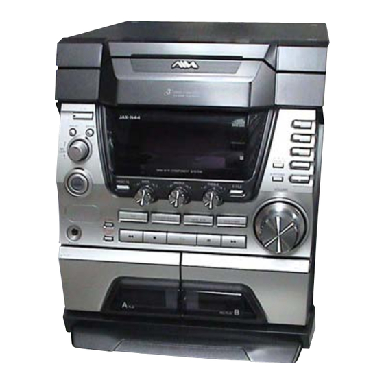
Page 7: General
CX-JN44 SECTION 2 This section is extracted from instruction manual. GENERAL • LOCATION OF CONTROLS Main unit ALPHABETICAL ORDER BUTTON DESCRIPTIONS ?/1 (power) 1 A – N O – Z Z PUSH (deck A) (eject) 0 BASS control 5 Operation Dial... -
Page 8: Setting The Clock
CX-JN44 Setting the clock Remote control ALPHABETICAL ORDER BUTTON DESCRIPTIONS Use buttons on the remote for the operation. ?/1 (power) 1 A – E F – Z Press ?/1 to turn on the system. m/M (rewind/fast forward) CD qk FM MODE 4 Press CLOCK/TIMER SET. -
Page 9: Disassembly Flow
CX-JN44 SECTION 3 DISASSEMBLY • This set can be disassembled in the order shown below. 3-1. DISASSEMBLY FLOW Note 1: The process described in can be performed in any order. Note 2: Without completing the process described in , the next process can not be performed. -
Page 10: Case (Side-L/R)
CX-JN44 Note: Follow the disassembly procedure in the numerical order given. 3-2. CASE (SIDE-L/R) 1 two screws (case 3 TP2) 3 two screws × (BVTP3 7 case (side-R) 2 screw (case 3 TP2) 4 case (side-L) 6 two screws ×... -
Page 11: Tray Panel
CX-JN44 3-4. TRAY PANEL four claws 3 Remove the tray panel 1 Turn the loading gear in the direction of arrow C . in the direction of arrow A . 2 Pull-out the tray in the direction of arrow B . -
Page 12: Front Panel Block
CX-JN44 3-6. FRONT PANEL BLOCK 1 wire (flat type) (29 core) (CN302) 2 connector 2 connector (CN103) (CN112) 6 front panel block 3 screw × (BVTP3 4 harness 2 connector (CN309) 5 three screws × (BVTP3 3-7. BACK PANEL SECTION... -
Page 13: Main Board
CX-JN44 3-8. MAIN BOARD 1 connector (CN907) 4 MAIN board 3 connector (CN307) 2 two screws × (BVTP3 3-9. TAPE MECHANISM DECK (CWM43FF13) 1 six screws × (BVTP2.6 2 tape mechanism deck (CWM43FF13) -
Page 14: Table Assy
CX-JN44 Ver. 1.2 3-10. TABLE ASSY 5 two claws 4 hook 3 wire (flat type) (5 core) (CN702) 1 Turn the loading gear 2 Pull-out the table assy. in the direction of arrow A . 6 table assy 3-11. MOTOR (TB) BOARD 1 screw (PTPWH M2.6) -
Page 15: Motor (Ld) Board
CX-JN44 3-12. MOTOR (LD) BOARD 3 two screws (BTTP M2.6) 4 MOTOR (LD) board 2 connector (CN704) 1 belt (loading) 3-13. BASE UNIT (BU-K6BD80A) 9 base unit (BU-K6BD80A) 1 wire (flat type) (27 core) (CN201) 5 three insulators 4 three coil springs... -
Page 16: Motor Gear Assy (Sled) (M102), Cd Board
CX-JN44 3-14. MOTOR GEAR ASSY (SLED) (M102), CD BOARD 7 gear (A) 6 claw 8 gear (B) 2 two screws (P2 × 3) 5 wire (flat type) (16 core) (CN101) qa CD board 0 motor gear assy (SLED) (M102) 1 Remove two solders. -
Page 17: Test Mode
CX-JN44 SECTION 4 TEST MODE MC COLD RESET CD TRAY LOCK MODE • The cold reset clears all data including preset data stored in • This mode is used to unable to take sample disc out of tray in the RAM to initial conditions. Execute this mode when the shop. - Page 18 CX-JN44 AGING MODE 3. Tape Deck Section • This mode can be used for operation check of CD section and The sequence during the aging mode is following as below. tape deck section. If an error occurred, stop display that step.
- Page 19 CX-JN44 MC TEST MODE 1. Mechanism Deck Error Code Mode • This mode is used to check operations of microprocessor. • When this mode is entered, mechanism deck error code is Procedure: displayed with the 10-character format on the fluorescent 1.
- Page 20 CX-JN44 The 7th and 8th digit from the left indicates: The 5th and 6th digit from the left indicates: (Motor status display) (Error step display) The 7th and 8th digit from the left indicates which motor output The 5th and 6th digit from the left indicates which processing when status when an error occurred is indicated.
-
Page 21: Electrical Check
CX-JN44 SECTION 5 ELECTRICAL CHECK Note: 1. CD Block is basically constructed to operate without adjustment. 2. Use YEDS-18 disc (3-702-101-01) unless otherwise indicated. 3. Use an oscilloscope with more than 10 MΩ impedance. 4. Clean the object lens by an applicator with neutral detergent when the signal level is low than specified value with the following checks. -
Page 22: Block Diagram – Servo Section
CX-JN44 SECTION 6 DIAGRAMS 6-1. BLOCK DIAGRAM – SERVO Section – FILTER XTSL CD DSP XTAO IC101 (1/2) CLOCK X171 48 50 47 49 DETECTOR CD +3V XTAI GENERATOR 16.9344MHz XTACN RFACI AOUT1 RFAC RFACO ASYMMETRY (Page 23) SUMMING DIGITAL PLL... -
Page 23: Block Diagram – Main Section
CX-JN44 6-2. BLOCK DIAGRAM – MAIN Section – JK101 63 MD L VIDEO/MD –1 R-CH LINE AMP TONE OUT1 36 VIN1 VOL OUT1 POWER IC102 JK441 – SPEAKER (Page 22) IC441 1 CD L IMPEDANCE –2 R-CH USE 6 – 16Ω... -
Page 24: Block Diagram Panel/Power Supply Section
CX-JN44 6-3. BLOCK DIAGRAM – PANEL/POWER SUPPLY Section – MAIN POWER TRANSFORMER SYSTEM CONTROLLER PT901 IC601 (3/3) AMP B+ +1.5V RECT CD +1.5V REGULATOR D401 AMP B– IC303 LED601 +3.3V O-POWER LED 76 S1 – 21 REGULATOR CD +3V D314, 315... - Page 25 CX-JN44 • Circuit Boards Location NOTE FOR PRINTED WIRING BOARDS AND SCHEMATIC DIAGRAMS Note on Printed Wiring Board: Note on Schematic Diagram: • X : parts extracted from the component side. • All capacitors are in µF unless otherwise noted. (p: pF) SUB TRANS board •...
-
Page 26: Printed Wiring Board – Bd Board
CX-JN44 • See page 25 for Circuit Boards Location. 6-4. PRINTED WIRING BOARD – BD Board – :Uses unleaded solder. OPTICAL PICK-UP BLOCK (KSM-213DAP) BD BOARD C116 C123 JW118 JR109 C122 C117 JR108 R121 R131 JR105 R111 JR111 R112 C131... -
Page 27: Schematic Diagram – Bd Board
CX-JN44 6-5. SCHEMATIC DIAGRAM – BD Board – CN201 XTACN TP29 XTACN C201 C182 C181 AGND DOUT TP31 DOUT R161 AVDD R201 TP32 AVDD LOUT TP33 LOUT AGND TP30 AGND ROUT TP34 ROUT C203 C202 C162 DGND TP35 DGND C213... -
Page 28: Printed Wiring Boards – Changer Section
CX-JN44 • See page 25 for Circuit Boards Location. 6-6. PRINTED WIRING BOARDS – CHANGER Section – :Uses unleaded solder. SW BOARD SENSOR BOARD CN751 IC731 S751 MAIN BOARD OPEN/CLOSE CN301 DETECT (Page 36) DRIVER BOARD CLOSE C715 OPEN Q731... -
Page 29: Schematic Diagram – Changer Section
CX-JN44 6-7. SCHEMATIC DIAGRAM – CHANGER Section – LOADING MOTOR DRIVE IC701 BA6956AN R702 R701 CN721 CN704 LM-2 LM-2 D701 M751 C751 LM-1 LM-1 MTZJ-T-77 0.01 (LOADING) 5.1A S711 DISC TRAY ADDRESS DETECT CN703 TABLE MOTOR DRIVE IC712 BA6956AN R712 R711 4.7k... -
Page 30: Printed Wiring Board Cdmp3 Connect Board
CX-JN44 • See page 25 for Circuit Boards Location. 6-8. PRINTED WIRING BOARD – CDMP3 CONNECT Board – :Uses unleaded solder. CDMP3 CONNECT BOARD BD BOARD CN201 (Page 26) JW866 CN872 JW865 JW861 JW862 JW863 CN874 MAIN BOARD CN305 (Page 36) -
Page 31: Schematic Diagram Cdmp3 Connect Board
CX-JN44 6-9. SCHEMATIC DIAGRAM – CDMP3 CONNECT Board – CN874 M+7V M-GND R-OUT JW865 A-GND L-OUT JW862 D-GND JW866 D-OUT JW863 FB871 AVDD (Page 34) JW864 FB872 DVDD JW876 CN872 M+7V MGND(7V) SCOR CN873 SENS CD-CLK SENS DATA CD-DATA XRST... -
Page 32: Schematic Diagram – Main Section (1/4)
CX-JN44 6-10. SCHEMATIC DIAGRAM – MAIN Section (1/4) – (1/4) JK101 R143 C138 C137 VIDEO/MD C147 R144 R136 R135 C145 4.7k 4.7k R131 C142 C141 R134 R133 R129 4.7k 4.7k R145 C171 R146 C172 100k 470p 100k 470p R130 Q106... -
Page 33: Schematic Diagram – Main Section (2/4)
CX-JN44 6-11. SCHEMATIC DIAGRAM – MAIN Section (2/4) – (2/4) CN101 LC72121 CLK LC72121 DO LC72121 DI FM 75Ω LC72121 CE R358 COAXIAL FM/AM R253 C253 TUNER PACK R262 TUNED TUNED 3.3k R263 R354 SUPPLIED WITH 4.7k Q352 STEREO STEREO... -
Page 34: Schematic Diagram – Main Section (3/4)
CX-JN44 6-12. SCHEMATIC DIAGRAM – MAIN Section (3/4) – (Page 32) (3/4) CN307 SP L-OUT SP-GND SP R-OUT RELAY B+ PROTECT PROTECTOR R-OUT ROUT A-GND L-OUT LOUT +16V PW-GND (Page 41) STK MUTE STK MUTE C217 R391 R392 R393 R394... -
Page 35: Schematic Diagram – Main Section (4/4)
CX-JN44 • See page 47 for IC Pin Function Description. 6-13. SCHEMATIC DIAGRAM – MAIN Section (4/4) – (Page 32) (Page 33) (4/4) R308 2.2k STK MUTE Q308 +3.3V REGULATOR R310 R306 2SA1235 IC301 POWER AMP TA78033LS D301 ON/OFF 10EDB40... -
Page 36: Printed Wiring Boards – Main Section
CX-JN44 • See page 25 for Circuit Boards Location. 6-14. PRINTED WIRING BOARDS – MAIN Section – :Uses unleaded solder. • Semiconductor Location Ref. No. Location MAIN BOARD D201 D202 H-10 D206 I-10 D207 H-10 JW146 D211 FM/AM DRIVE BOARD... -
Page 37: Printed Wiring Board – Panel Section
CX-JN44 • See page 25 for Circuit Boards Location. 6-15. PRINTED WIRING BOARD – PANEL Section – :Uses unleaded solder. PANEL BOARD C622 R786 LED601 LED601, S601 R684 JW708 JR615 R719 C623 C620 R645 R683 R629 R716 R718 Q616 D605... -
Page 38: Schematic Diagram – Panel Section (1/2)
CX-JN44 • See page 48 for IC Pin Function Description. 6-16. SCHEMATIC DIAGRAM – PANEL Section (1/2) – (1/2) FL601 FLUORESCENT INDICATOR TUBE C622 R719 C621 3.3k 0.022 C642 C641 R771 R718 LED601 SLI-325URC R717 R772 3.3k R716 C620 C623... -
Page 39: Schematic Diagram – Panel Section (2/2)
CX-JN44 6-17. SCHEMATIC DIAGRAM – PANEL Section (2/2) – (2/2) S661 AMS/ S660 TUNING VOLUME R701 R702 R710 R712 R703 R704 R711 R713 C650 C651 C617 C618 1000p 1000p 1000p 1000p R651 R650 R649 R648 R647 R646 R645 R644 R643 R642 6.8k... -
Page 40: Printed Wiring Board – Power Amp Section
CX-JN44 • See page 25 for Circuit Boards Location. • Semiconductor 6-18. PRINTED WIRING BOARD – POWER AMP Section – :Uses unleaded solder. Location Ref. No. Location D401 D441 D442 D443 JK441 D481 SPEAKER D482 IMPEDANCE – – USE 6 – 16Ω... -
Page 41: Schematic Diagram – Power Amp Section
CX-JN44 6-19. SCHEMATIC DIAGRAM – POWER AMP Section – TH441 JW403 JK441 Q481,482 L441 DC DETECT R461 RY441 10 1/2W R466 SPEAKER IMPEDANCE POWER AMP R411 Q482 Q481 R462 USE 6−16Ω 2.2k IC441(1/2) 2SC2785 2SC2785 10 1/2W STK403-130 R451 0.22... -
Page 42: Printed Wiring Boards – Trans Section
CX-JN44 • See page 25 for Circuit Boards Location. 6-20. PRINTED WIRING BOARDS – TRANS Section – :Uses unleaded solder. SUB TRANS BOARD TRANS BOARD D904 D905 C904 C903 D902 D903 JW918 CN906 C905 CN902 R902 PT902 SUB POWER CN904... -
Page 43: Schematic Diagram – Trans Section
CX-JN44 6-21. SCHEMATIC DIAGRAM – TRANS Section – CN905 F904 125V AC-1 PT901 AC-1 MAIN POWER TRANSFORMER F905 (Page 41) 125V JW902 F906 CN903 3.15A CN904 CN907 125V NEUTRAL LIVE JW909 PT902 SUB POWER RY901 TRANSFORMER JW910 F907 3.15A 125V... - Page 44 CX-JN44 • Waveforms • IC Block Diagrams – BD Board – – MAIN Board – – PANEL Board – – BD Board – IC101 w; (TEI) L101 5 (Rec Mode) IC601 qd (I-XT2) IC101 CXD3058AR (CD Play Mode) Approx. 3.2 Vp-p...
- Page 45 CX-JN44 IC251 BA5947FM MUTING + – INTERFACE LEVEL SHIFT INTERFACE INTERFACE VREF – DRIVER Board – IC701, 702 BA6956AN CONTROL LOGIC – MAIN Board – IC201 BA3126N...
- Page 46 CX-JN44 IC101 BD3401KS2 56 55 54 53 52 51 48 MNF2 SOFT 47 MOUT2 SWITCH 46 MOUT1 45 MNF1 44 BNF1 43 BOUT1 − 42 BOUT2 41 BNF2 INPUT SELECT − PBNF2 PBOUT2 BUFFER PBOUT1 − MIC AMP PBNF1 40 AMS OUT...
-
Page 47: Ic Pin Function Description
CX-JN44 6-22. IC PIN FUNCTION DESCRIPTION • MAIN BOARD IC371 BU2099FV (LOADING/TABLE MOTOR DRIVER) Pin No. Pin Name Description — Ground terminal N.C. — Not used DATA Serial data input from the system controller CLOCK Serial data transfer clock signal input from the system controller... - Page 48 CX-JN44 • PANEL BOARD IC601 LC876964C-53V9-E (SYSTEM CONTROLLER) Pin No. Pin Name Description O-MP3 CS Capstan/reel motor drive signal output terminal O-MP3 LP Plunger (deck-B) drive signal output terminal I-MP3 ACK Plunger (deck-A) drive signal output terminal I-MP3 REQ Request signal input terminal Not used...
- Page 49 CX-JN44 Pin No. Pin Name Description VDD4 — Power supply terminal (+3.3V) I-CD NUM CD table address detection signal input terminal SENSOR O-POWER RELAY Power on/off control signal output terminal “H”: power on O-SYSTEM-MUTE System muting on/off control signal output terminal “H”: muting on O-POWER LED LED drive signal output of the I/1 (power) indicator “H”: LED on...
-
Page 50: Case Section
CX-JN44 SECTION 7 EXPLODED VIEWS NOTE: • -XX and -X mean standardized parts, so they • The mechanical parts with no reference The components identified by mark 0 or may have some difference from the original number in the exploded views are not supplied. -
Page 51: Tape Mechanism Deck Section (Cwm43Ff13)
CX-JN44 7-2. TAPE MECHANISM DECK SECTION (CWM43FF13) not supplied (HEADPHONE board) cassette box section Ref. No. Part No. Description Remark Ref. No. Part No. Description Remark 4-252-707-01 KNOB (VOL), PLATING ROTARY 1-827-145-11 WIRE (FLAT TYPE) (13 CORE) 4-252-709-01 KNOB (AMS), PLATING ROTARY... -
Page 52: Cassette Box Section
CX-JN44 7-3. CASSETTE BOX SECTION front panel section Ref. No. Part No. Description Remark Ref. No. Part No. Description Remark 4-252-715-01 SPRING (BOX CASS L), TORSION 4-224-104-41 DAMPER 4-252-698-01 WINDOW (L), CASSETTE 4-231-841-01 SPRING (HEART CAM-B) 4-252-695-01 BOX (L), CASSETTE... -
Page 53: Front Panel Section
CX-JN44 7-4. FRONT PANEL SECTION not supplied not supplied not supplied not supplied not supplied not supplied not supplied Ref. No. Part No. Description Remark Ref. No. Part No. Description Remark 4-252-697-21 WINDOW, DISPLAY 4-218-253-72 +BTTP M2.6 4-252-776-01 KNOB (BASS), ROTARY... -
Page 54: Back Panel Section
CX-JN44 7-5. BACK PANEL SECTION not supplied not supplied M901 not supplied (SUB TRANS board) not supplied chassis section Ref. No. Part No. Description Remark Ref. No. Part No. Description Remark 1-769-940-11 WIRE (FLAT TYPE) (11 CORE) 7-685-647-79 SCREW +BVTP 3X10 TYPE2 IT-3... -
Page 55: Chassis Section
CX-JN44 7-6. CHASSIS SECTION not supplied F904 F905 F906 F907 PT901 not supplied supplied not supplied Ref. No. Part No. Description Remark Ref. No. Part No. Description Remark 4-900-386-01 SCREW 4-059-585-01 TIE, CABLE 0 F904 3-703-244-00 BUSHING (2104), CORD 1-576-537-12 FUSE, GLASS TUBE (DIA. 5) (8A/125V) -
Page 56: Cd Mechanism Deck Section-1 (Cdm74-K6Bd80)
CX-JN44 Ver. 1.2 7-7. CD MECHANISM DECK SECTION-1 (CDM74-K6BD80) M741 CD mechanism deck section -2 Ref. No. Part No. Description Remark Ref. No. Part No. Description Remark 4-243-816-01 TRAY 1-687-134-12 MOTOR (TB) BOARD 4-218-252-61 SCREW (+PTPWH M2.6), FLOATING 4-243-815-01 TABLE (LOADING) 4-218-253-21 SCREW (M2.6), +BTTP... -
Page 57: Cd Mechanism Deck Section-2 (Cdm74-K6Bd80)
CX-JN44 7-8. CD MECHANISM DECK SECTION-2 (CDM74-K6BD80) S711 M751 CD mechanism deck section -3 Ref. No. Part No. Description Remark Ref. No. Part No. Description Remark 4-218-252-61 SCREW (+PTPWH M2.6), FLOATING 3-016-533-11 WASHER (FR), STOPPER 4-244-034-01 BELT (LOADING) 4-244-108-01 GEAR, SWING... -
Page 58: Cd Mechanism Deck Section-3 (Cdm74-K6Bd80)
CX-JN44 7-9. CD MECHANISM DECK SECTION-3 (CDM74-K6BD80) BU-K6BD80A Ref. No. Part No. Description Remark Ref. No. Part No. Description Remark X-4955-707-2 PULLEY (A5) ASSY, CHUCKING 4-227-549-11 INSULATOR 1-471-035-11 MAGNET ASSY 4-227-045-31 SPRING (INSULATOR), COIL 4-231-189-01 PULLEY (B), CHUCKING 4-231-151-01 STOPPER (BU) 4-218-252-61 SCREW (+PTPWH M2.6), FLOATING... -
Page 59: Base Unit Section (Bu-K6Bd80A)
CX-JN44 7-10. BASE UNIT SECTION (BU-K6BD80A) (including M101 (spindle), M102 (sled)) not supplied not supplied not supplied not supplied M101(spindle) not supplied not supplied not supplied not supplied not supplied M102 (sled) S101 Ref. No. Part No. Description Remark Ref. No. -
Page 60: Electrical Parts List
CX-JN44 SECTION 8 ELECTRICAL PARTS LIST NOTE: • Due to standardization, replacements in the • COILS When indicating parts by reference number, parts list may be different from the parts uH: µH please include the board name. specified in the diagrams or the components •... - Page 61 CX-JN44 COMP3 CONNECT DRIVER HEADPHONE Ref. No. Part No. Description Remark Ref. No. Part No. Description Remark 1-218-446-11 METAL CHIP 1/10W 1-687-135-12 DRIVER BOARD R111 1-216-821-11 METAL CHIP 1/10W ************* R112 1-216-835-11 METAL CHIP 1/10W < CAPACITOR > R113 1-216-821-11 METAL CHIP...
- Page 62 CX-JN44 MAIN Ref. No. Part No. Description Remark Ref. No. Part No. Description Remark A-4750-685-A MAIN BOARD, COMPLETE C159 1-126-960-11 ELECT C160 1-126-960-11 ELECT ********************* C165 1-126-960-11 ELECT 7-685-872-09 SCREW +BVTT 3X8 (S) C166 1-126-960-11 ELECT < CAPACITOR > C167...
- Page 63 CX-JN44 MAIN Ref. No. Part No. Description Remark Ref. No. Part No. Description Remark C301 1-136-165-00 FILM 0.1uF D310 6-500-522-21 DIODE 10EDB40-TB3 C302 1-136-165-00 FILM 0.1uF D311 6-500-522-21 DIODE 10EDB40-TB3 C303 1-136-165-00 FILM 0.1uF D312 6-500-522-21 DIODE 10EDB40-TB3 C304 1-136-165-00 FILM 0.1uF...
- Page 64 CX-JN44 MAIN Ref. No. Part No. Description Remark Ref. No. Part No. Description Remark Q314 6-550-580-01 TRANSISTOR 2SA1235TP-1F R157 1-216-841-11 METAL CHIP 1/10W Q315 8-729-120-28 TRANSISTOR 2SC1623-L5L6 Q321 8-729-142-46 TRANSISTOR 2SC2001-LK R158 1-216-825-11 METAL CHIP 2.2K 1/10W R159 1-216-833-11 METAL CHIP...
- Page 65 CX-JN44 MAIN MOTOR (LD) MOTOR (TB) PANEL Ref. No. Part No. Description Remark Ref. No. Part No. Description Remark R232 1-216-833-11 METAL CHIP 1/10W R361 1-216-833-11 METAL CHIP 1/10W R235 1-216-793-11 METAL CHIP 1/10W R362 1-216-825-11 METAL CHIP 2.2K 1/10W...
- Page 66 CX-JN44 PANEL Ref. No. Part No. Description Remark Ref. No. Part No. Description Remark C618 1-162-964-11 CERAMIC CHIP 0.001uF D630 8-719-988-61 DIODE 1SS355TE-17 C619 1-126-947-11 ELECT 47uF D631 8-719-978-33 DIODE DTZ-TT11-6.8B C620 1-126-947-11 ELECT 47uF D632 8-719-083-57 DIODE UDZSTE-173.6B C621 1-162-995-11 CERAMIC CHIP 0.022uF...
- Page 67 CX-JN44 PANEL Ref. No. Part No. Description Remark Ref. No. Part No. Description Remark R607 1-216-841-11 METAL CHIP 1/10W R674 1-216-835-11 METAL CHIP 1/10W R608 1-216-829-11 METAL CHIP 4.7K 1/10W R675 1-216-835-11 METAL CHIP 1/10W R609 1-216-837-11 METAL CHIP 1/10W...
- Page 68 CX-JN44 PANEL POWER Ref. No. Part No. Description Remark Ref. No. Part No. Description Remark R742 1-216-845-11 METAL CHIP 100K 1/10W S603 1-762-875-21 SWITCH, KEYBOARD (ENTER) R743 1-216-845-11 METAL CHIP 100K 1/10W S604 1-762-875-21 SWITCH, KEYBOARD (DISC 1) R744 1-216-845-11 METAL CHIP...
- Page 69 CX-JN44 POWER Ref. No. Part No. Description Remark Ref. No. Part No. Description Remark C448 1-126-965-11 ELECT 22uF R402 1-247-879-91 CARBON 100K 1/4W C451 1-136-497-81 FILM 0.1uF R407 1-260-316-51 CARBON 1/2W C452 1-136-497-81 FILM 0.1uF R411 1-249-421-11 CARBON 2.2K 1/4W...
- Page 70 CX-JN44 Ver 1.1 SENSOR SUB TRANS TRANS Ref. No. Part No. Description Remark Ref. No. Part No. Description Remark 1-687-132-12 SENSOR BOARD < CONNECTOR > ************* CN904 1-564-321-00 PIN, CONNECTOR (3.96mm PITCH) 2P < CONNECTOR > CN905 1-564-506-11 PLUG, CONNECTOR 3P...
- Page 71 CX-JN44 MEMO...
-
Page 72: Revision History
CX-JN44 REVISION HISTORY Clicking the version allows you to jump to the revised page. Also, clicking the version at the upper right on the revised page allows you to jump to the next revised page. Ver. Date Description of Revision 2004.04...
Need help?
Do you have a question about the CX-JN44 and is the answer not in the manual?
Questions and answers