
Related Manuals for Samsung SGH-P270


Summary of Contents for Samsung SGH-P270
-
Page 1: Table Of Contents
GSM TELEPHONE SGH-P270 GSM TELEPHONE CONTENTS 1. Safety Precautions 2. Specification 3. Product Function 4. Array course control 5. Exploded View and Parts list 6. MAIN Electrical Parts List 7. Disassembly and Assembly Instructions 8. Block Diagrams 9. PCB Diagrams 10. - Page 2 China china.samsungportal.com Asia asia.samsungportal.com Mideast & Africa mea.samsungportal.com This Service Manual is a property of Samsung Electronics Co.,Ltd. Samsung Electronics Co.,Ltd. ⓒ Any unauthorized use of Manual can be punished under applicable International and/or domestic law. 2008. 11. Rev.1.0...
-
Page 3: Specification
5pcl ~ 19pcl 0pcl ~ 15pcl 0pcl ~ 15pcl Sensitivity - 102dBm - 102dBm - 100dBm - 100dBm TDMA M ux Cell Radius 35Km 35 Km SAMSUNG Proprietary-Contents may change without notice This Document can not be used without Samsung's authorization... -
Page 4: Gsm Tx Power Class
11±5 dBm 8±4dBm 8±4dBm 9±5 dBm 6±4 dBm 6±4 dBm 7±5 dBm 4±4 dBm 4±4 dBm 5±5 dBm 2±5 dBm 2±5 dBm 0±5 dBm 0±5 dBm SAMSUNG Proprietary-Contents may change without notice This Document can not be used without Samsung's authorization... - Page 5 14±3 dBm 9±5 dBm 12±4 dBm 12±4 dBm 10±4 dBm 7±5 dBm 10±4 dBm 8±4dBm 5±5 dBm 8±4dBm 6±4 dBm 6±4 dBm 4±4 dBm 4±4 dBm SAMSUNG Proprietary-Contents may change without notice This Document can not be used without Samsung's authorization...
-
Page 6: Product Function
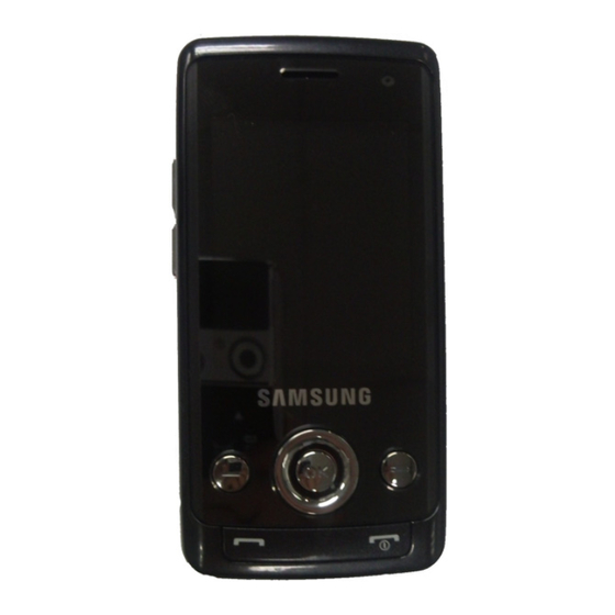
- LCD : 2.2”, 176x220, 262K TFT - Size: 99 x 49 x 14.9 mm (TBD) - Band: 900/1800/1900/2100 - BB : PNX 5217 (NXP) - RF : UAA3582(3G) + SI4221(2G) SAMSUNG Proprietary-Contents may change without notice This Document can not be used without Samsung's authorization... -
Page 7: Reference Abbreviate
― QPSK: Quadrature Phase Shift Keying ― RS : Reed-Solomon ― SI : Service Information ― TDM : Time Division Multiplexing ― TS : Transport Stream 10-1 SAMSUNG Proprietary-Contents may change without notice This Document can not be used without Samsung's authorization... -
Page 8: Safety Precautions
― Don't use as you pleases after change other material than replacement registered on SEC System. Otherwise engineer in charge isn't charged with problem that you don't keep this rules. SAMSUNG Proprietary-Contents may change without notice This Document can not be used without Samsung's authorization... - Page 9 ― You must maintain electric contact between ESD and place due to be set up until ESD is connected completely to the proper place or a circuit board. SAMSUNG Proprietary-Contents may change without notice This Document can not be used without Samsung's authorization...
-
Page 10: Exploded View And Parts List
QCR12 QKP02 QMP01 QCA01 QCA02 QME02 QAN02 QMI01 QAR01 QLC01 QMO01 QSP01 QSH01 QPC01 QAN03 QCO01 QIF01 QCR17 QCK01 QFL01 QRE01 QCH05 QCR03 QBA01 QBA00 SAMSUNG Proprietary-Contents may change without notice This Document can not be used without Samsung's authorization... -
Page 11: Main Electrical Parts List
QMI03 ASSY RUBBER-MIC GH98-09878A QRE01 ASSY CASE-REAR GH98-09063C QCH05 PMO COVER-T FLASH GH72-48581C QCK01 PMO KEY-CAMERA GH72-48582A QIF01 PMO COVER-IF GH72-48580C QVO01 ASSY KEY-VOLUME GH98-10799A SAMSUNG Proprietary-Contents may change without notice This Document can not be used without Samsung's authorization... -
Page 12: Disassembly And Assembly Instructions
1) Unscrew the 4 points. 2) Separate the FRONT case from the slide ass'y. ※ Caution ※ Caution 1) Be care of scratch and molding damage. 11-1 SAMSUNG Proprietary-Contents may change without notice This Document can not be used without Samsung's authorization... - Page 13 2) Disassemble the VGA F-PCB from the sub PCB. ※ Caution ※ Caution ) Be care of damage to camera F-PCB. Be care of scratch to main WINDOW. 11-2 SAMSUNG Proprietary-Contents may change without notice This Document can not be used without Samsung's authorization...
- Page 14 1) Unscrew the 2 points to separate the INTENNA from the PBA. shield can from the PBA. ※ Caution ※ Caution 1) Be care of scratch and molding damage. 11-3 SAMSUNG Proprietary-Contents may change without notice This Document can not be used without Samsung's authorization...
- Page 15 1) Screw down the 1 point ※ Caution ※ Caution 1) Be care of damage the INTENNA. 1) Be care of damage the F-PCB and connector. 11-4 SAMSUNG Proprietary-Contents may change without notice This Document can not be used without Samsung's authorization...
- Page 16 1) Be care of damage to the VGA F-PCB. 2) Keep clean the main WINDOW before assembling 2) Wires shold be arranged like the picture. the LCD module. 11-5 SAMSUNG Proprietary-Contents may change without notice This Document can not be used without Samsung's authorization...
- Page 17 1) Screw down the 4 points. 1) Place the KEYPAD on the FRONT case. ※ Caution ※ Caution 1) Be care of scratch and molding damage. 11-6 SAMSUNG Proprietary-Contents may change without notice This Document can not be used without Samsung's authorization...
- Page 18 ※ Caution ※ Caution 1) Be care of scratch and damage to the slide 1) Be care of scratch and molding damage. F-PCB. 11-7 SAMSUNG Proprietary-Contents may change without notice This Document can not be used without Samsung's authorization...
- Page 19 Check the VDD_GSM_CORE_1.2V circuit = 1.2V? Check the clock generation circuit Check for the clock at TCX100 = 26MHz (related to TCX100) Check the initial operation SAMSUNG Proprietary-Contents may change without notice This Document can not be used without Samsung's authorization...
- Page 20 C430 VREF_3G_B1 GPO1 GPO2 R421 ADV3V VINT VINT VCC_TX GPO1VIN GPO2VIN C432 32KHZ_DIGIT CLK32K OSCI OSCO OSC400 L402 VDD_GSM_CORE L403 VDD_MEM_3G_CORE VBAT C442 C443 C444 SAMSUNG Proprietary-Contents may change without notice This Document can not be used without Samsung's authorization...
- Page 21 Flow Chart of Troubleshooting SAMSUNG Proprietary-Contents may change without notice This Document can not be used without Samsung's authorization...
- Page 22 UCP300 pin A16 (RSTBB) Check the circuit related to reset ="H"? UCP300 pin AC4 change UCP300 (RSTEXTn) ="H"? Check the 16bit data signal & memory CE SAMSUNG Proprietary-Contents may change without notice This Document can not be used without Samsung's authorization...
- Page 23 AD25 FCI_CLK GPIOB9 MCLKSEL AA25 FCI_DATA0 GPIOB10 IOM_DCL AB24 Y(7) GPIOB11 IOM_DD TP333 AB25 GPIOB13 IOM_FSC TP334 GPIOB14 VREF TP335 GPIOB15 VDD_IO_LOW C348 C349 IOM_DU SAMSUNG Proprietary-Contents may change without notice This Document can not be used without Samsung's authorization...
-
Page 24: Sim Part
Check SIMCLK Signal on Check the Clock of SIM500 in a few second After SIM card insert, Resolder or replace UCP300 SIM500 = "H(SIMRST)"? Check the SIM Card SAMSUNG Proprietary-Contents may change without notice This Document can not be used without Samsung's authorization... - Page 25 FCI_CMD FCI_CLK FCI_DATA0 10 8 FCI_DATA1 12 C5 SIMRSTn 14 C6 15 C3 SIMCLK SIMIO 19 NC 21 NC 23 NC C514 C515 U514 U515 SAMSUNG Proprietary-Contents may change without notice This Document can not be used without Samsung's authorization...
-
Page 26: Charging Part
Abnormal charging part Check the circuit related to Check the U400 pin A53,A54,A55 > 4.9V VCHG_5V Check the circuit related to U400 D5(AUX_ON) = "L"? AUX_ON signal SAMSUNG Proprietary-Contents may change without notice This Document can not be used without Samsung's authorization... - Page 27 C430 VREF_3G_B1 GPO1 GPO2 R421 ADV3V VINT VINT VCC_TX GPO1VIN GPO2VIN C432 32KHZ_DIGIT CLK32K OSCI OSCO OSC400 L402 VDD_GSM_CORE L403 VDD_MEM_3G_CORE VBAT C442 C443 C444 SAMSUNG Proprietary-Contents may change without notice This Document can not be used without Samsung's authorization...
-
Page 28: Microphone Part
C408, C421, L400, L401 from UCP300 to MIC Check IFC500 PIN 9 Check the JACK_IN signal = ' H' ? Check the MIC Replace the MIC 9-10 SAMSUNG Proprietary-Contents may change without notice This Document can not be used without Samsung's authorization... - Page 29 TXD1 R509 RXD1 R531 AUX_ON R510 USBDP R512 17 17 USBDM 19 19 22 NC 23 NC 25 NC D503 D512 C504 D516 D517 9-11 SAMSUNG Proprietary-Contents may change without notice This Document can not be used without Samsung's authorization...
- Page 30 Flow Chart of Troubleshooting 9-12 SAMSUNG Proprietary-Contents may change without notice This Document can not be used without Samsung's authorization...
-
Page 31: Speaker Part
Resolder or replace UCP300 C1(EAR2) & C2(EAR1) Is there any signal at Resolder or replace U402 B5(OUT+) & D5(OUT-) Change the Speaker Is Speaker working? 9-13 SAMSUNG Proprietary-Contents may change without notice This Document can not be used without Samsung's authorization... - Page 32 AMP_P INA1 EARSPK_R C451 AMP_N INA2 EARSPK_L U402 C452 EAR1 INB1 C453 C460 C461 EAR2 INB2 ZD400 ZD401 BIAS SDA1 SCL1 C455 C456 C459 9-14 SAMSUNG Proprietary-Contents may change without notice This Document can not be used without Samsung's authorization...
-
Page 33: Receiver Part
Receiver does not work Is there any signal at Resolder UCP300 or change PBA HDC500 pin 11(RCV_P) & 13(RCV_N) Replace the Receiver Is Receiver working? 9-15 SAMSUNG Proprietary-Contents may change without notice This Document can not be used without Samsung's authorization... - Page 34 L E D50 0 L E D50 1 R52 6 V T CALL S WI T C H CL R S T A R SHARP 9-16 SAMSUNG Proprietary-Contents may change without notice This Document can not be used without Samsung's authorization...
- Page 35 IFC500 pin 5,6,7 short? Is there any signal at IFC500 Resolder the R506, R 507 pin 5, 7 Is Earphone working? Replace the earphone 9-17 SAMSUNG Proprietary-Contents may change without notice This Document can not be used without Samsung's authorization...
- Page 36 TXD1 R509 RXD1 R531 AUX_ON R510 USBDP R512 17 17 USBDM 19 19 22 NC 23 NC 25 NC D503 D512 C504 D516 D517 9-18 SAMSUNG Proprietary-Contents may change without notice This Document can not be used without Samsung's authorization...
- Page 37 Flow Chart of Troubleshooting 9-19 SAMSUNG Proprietary-Contents may change without notice This Document can not be used without Samsung's authorization...
- Page 38 Check the U503, PEMD10 C521 = 2.9V Check HDC501(pin12, 13) related to 39MHz HDC 501 pin 12, 13 = 39Mhz? UCP300 Replace the New Camera & END 9-20 SAMSUNG Proprietary-Contents may change without notice This Document can not be used without Samsung's authorization...
- Page 39 18 18 SCL2 SDA2 2 GND CAM_RST VOUT2 21 21 MCAM_SLEEP C521 C517 CAM_PD CAM_PD C519 R539 C522 C523 C520 C518 C525 C526 C524 9-21 SAMSUNG Proprietary-Contents may change without notice This Document can not be used without Samsung's authorization...
- Page 40 L200, C205, C206 PAM200 PIN9 Re-solder PAM200, ≥ -15dBm L215, C227, C214 U203 PIN4 Re-solder F202, ≥ -20dBm L208, L209, C220 Check U203 , UCP300 9-22 SAMSUNG Proprietary-Contents may change without notice This Document can not be used without Samsung's authorization...
- Page 41 L207 ITX_N L208 L209 C223 ITX_P C224 VCC_TX VCC2 RFIN VCC2 C226 PAM200 C227 VCC2 VMODE RF_DAC2 9 RFOUT VREG C228 L215 VREF_3G_B1 C231 9-23 SAMSUNG Proprietary-Contents may change without notice This Document can not be used without Samsung's authorization...
- Page 42 Flow Chart of Troubleshooting 9-24 SAMSUNG Proprietary-Contents may change without notice This Document can not be used without Samsung's authorization...
- Page 43 ≥ -75dBm Re-solder or Change U203 PIN29 U203 ≥ -75dBm Re-solder or Change F200 PIN3,4 F200, C211, R202, R203, ≥ -75dBm L202 Check U203, UCP300 9-25 SAMSUNG Proprietary-Contents may change without notice This Document can not be used without Samsung's authorization...
- Page 44 Check MOD100 MOD100 PIN24 PIN15=H, PIN14=H ≥ -15dBm PIN13=L Re-solder or Change MOD 101 U100 PIN15 Re-solder C125, L207 ≥ -15dBm Check U100, UCP300 9-26 SAMSUNG Proprietary-Contents may change without notice This Document can not be used without Samsung's authorization...
- Page 45 MOD100 PIN22 PIN15=L, PIN14=H ≥ -15dBm PIN13=H Re-solder or Change MOD 100 U100 PIN17 Re-solder or Change ≥ -15dBm C122, L113 Check U100, UCP300 9-27 SAMSUNG Proprietary-Contents may change without notice This Document can not be used without Samsung's authorization...
- Page 46 MOD100 PIN3,4 PIN15=L, PIN14=L ≥ -70dBm PIN13=H Re-solder or Change MOD 100 Re-solder or U100 PIN24,25 Change ≥ -75dBm C104, C107, L100 Check U100, UCP300 9-28 SAMSUNG Proprietary-Contents may change without notice This Document can not be used without Samsung's authorization...
- Page 47 MOD100 PIN5,6 PIN15=L, PIN14=H ≥ -70dBm PIN13=H Re-solder or Change MOD100 Re-solder or Change U100 PIN22,23 C108, C111, L116 ≥ -75dBm Check U100, UCP300 9-29 SAMSUNG Proprietary-Contents may change without notice This Document can not be used without Samsung's authorization...
- Page 48 MOD100 PIN7,8 PIN15=L, PIN14=H ≥ -70dBm PIN13=L Re-solder or Change MOD100 Re-solder or Change U100 PIN20,21 C117, C119, L105 ≥ -75dBm Check U100, UCP300 9-30 SAMSUNG Proprietary-Contents may change without notice This Document can not be used without Samsung's authorization...
-
Page 49: Software Adjustments
4. Array course control 4-1. Software Adjustments Test Cable (GH39-01160A) Test Jig (GH99-36900A) RF Test Cable (GH39-00985A) Adapter (GH99-38251A) SAMSUNG Proprietary-Contents may change without notice This Document can not be used without Samsung's authorization... -
Page 50: Software Downloading
- if you want to download by RS232C, check only 'RS232C' - if you want to download by USB, check only 'USB' 3. Click the Partition Table. SAMSUNG Proprietary-Contents may change without notice This Document can not be used without Samsung's authorization... - Page 51 Array course control 4. Click the Browse and select your binary file. SAMSUNG Proprietary-Contents may change without notice This Document can not be used without Samsung's authorization...
-
Page 52: Block Diagrams
HB_RFIN BAND_SEL DVGA AVGA TX_EN Integrated VBATT DVGA AVGA Power Control VMODE XOUT RAMPOUT VRAMP VCO+FREQUENCY DCXO SYNTHESIZER CTRL LB_RFOUT 2G TRANSCEIVER HB_RFIN 26MHz (AERO4221) SAMSUNG Proprietary-Contents may change without notice This Document can not be used without Samsung's authorization... - Page 53 USBDP / USBDM / VBUS JACKIN KEY_ROW(0:4) FM_ANT VCHG SIMIO / SIMCLK / SIMRSTn Socket KEYPAD TXD1 / RXD1 VBUS KEY_COL(0:4) FCI_DATA / FCI_CLK / FCI_CMD T-FLASH ONKEYn FCI_CD SAMSUNG Proprietary-Contents may change without notice This Document can not be used without Samsung's authorization...
- Page 54 Block Diagrams 7-4. FM Radio Solution Block Diagram SAMSUNG Proprietary-Contents may change without notice This Document can not be used without Samsung's authorization...
- Page 55 D512 DIODE-TVS 0406-001281 D513 DIODE-TVS 0406-001281 D514 DIODE-TVS 0406-001281 D515 DIODE-TVS 0406-001321 D502 DIODE-TVS 0504-001151 TR500 TR-DIGITAL 0601-002048 LED500 0601-002048 LED501 1001-001453 U401 IC-ANALOG SWITCH SAMSUNG Proprietary-Contents may change without notice This Document can not be used without Samsung's authorization...
- Page 56 R-CHIP 2007-000148 R501 R-CHIP 2007-000148 R514 R-CHIP 2007-000148 R523 R-CHIP 2007-000148 R529 R-CHIP 2007-000148 R533 R-CHIP 2007-000149 R310 R-CHIP 2007-000152 R524 R-CHIP 2007-000157 R211 R-CHIP SAMSUNG Proprietary-Contents may change without notice This Document can not be used without Samsung's authorization...
- Page 57 R-CHIP 2007-001319 R314 R-CHIP 2007-001319 R315 R-CHIP 2007-001319 R316 R-CHIP 2007-001333 R500 R-CHIP 2007-001333 R502 R-CHIP 2007-001339 R503 R-CHIP 2007-002796 R208 R-CHIP 2007-003015 R201 R-CHIP SAMSUNG Proprietary-Contents may change without notice This Document can not be used without Samsung's authorization...
- Page 58 C-CER,CHIP 2203-000278 C203 C-CER,CHIP 2203-000278 C227 C-CER,CHIP 2203-000386 C210 C-CER,CHIP 2203-000386 C435 C-CER,CHIP 2203-000425 C432 C-CER,CHIP 2203-000438 C131 C-CER,CHIP 2203-000438 C218 C-CER,CHIP 2203-000438 C221 C-CER,CHIP SAMSUNG Proprietary-Contents may change without notice This Document can not be used without Samsung's authorization...
- Page 59 C-CER,CHIP 2203-002668 C205 C-CER,CHIP 2203-002668 C216 C-CER,CHIP 2203-002677 C159 C-CER,CHIP 2203-002709 C115 C-CER,CHIP 2203-002709 C134 C-CER,CHIP 2203-002709 C154 C-CER,CHIP 2203-002709 C155 C-CER,CHIP 2203-002709 C339 C-CER,CHIP SAMSUNG Proprietary-Contents may change without notice This Document can not be used without Samsung's authorization...
- Page 60 C-CER,CHIP 2203-005482 C330 C-CER,CHIP 2203-005482 C333 C-CER,CHIP 2203-005482 C334 C-CER,CHIP 2203-005571 C241 C-CER,CHIP 2203-005571 C242 C-CER,CHIP 2203-006048 C100 C-CER,CHIP 2203-006048 C126 C-CER,CHIP 2203-006048 C135 C-CER,CHIP SAMSUNG Proprietary-Contents may change without notice This Document can not be used without Samsung's authorization...
- Page 61 C-CER,CHIP 2203-006048 C514 C-CER,CHIP 2203-006048 C521 C-CER,CHIP 2203-006048 C523 C-CER,CHIP 2203-006257 C320 C-CER,CHIP 2203-006257 C321 C-CER,CHIP 2203-006257 C401 C-CER,CHIP 2203-006257 C407 C-CER,CHIP 2203-006257 C411 C-CER,CHIP SAMSUNG Proprietary-Contents may change without notice This Document can not be used without Samsung's authorization...
- Page 62 C-CER,CHIP 2203-006562 C149 C-CER,CHIP 2203-006562 C150 C-CER,CHIP 2203-006562 C430 C-CER,CHIP 2203-006562 C447 C-CER,CHIP 2203-006562 C454 C-CER,CHIP 2203-006562 C455 C-CER,CHIP 2203-006562 C456 C-CER,CHIP 2203-006562 C458 C-CER,CHIP SAMSUNG Proprietary-Contents may change without notice This Document can not be used without Samsung's authorization...
- Page 63 INDUCTOR-SMD 2703-001733 L210 INDUCTOR-SMD 2703-001734 L202 INDUCTOR-SMD 2703-001786 L205 INDUCTOR-SMD 2703-002155 L102 INDUCTOR-SMD 2703-002170 L113 INDUCTOR-SMD 2703-002200 L112 INDUCTOR-SMD 2703-002203 L103 INDUCTOR-SMD 2703-002207 L111 INDUCTOR-SMD SAMSUNG Proprietary-Contents may change without notice This Document can not be used without Samsung's authorization...
- Page 64 U302 BEAD-SMD 3301-001729 L400 BEAD-SMD 3301-001729 L401 BEAD-SMD 3301-001787 U504 CORE-FERRITE BEAD 3301-001787 U505 CORE-FERRITE BEAD 3301-001787 U506 CORE-FERRITE BEAD 3301-001787 U507 CORE-FERRITE BEAD 6-10 SAMSUNG Proprietary-Contents may change without notice This Document can not be used without Samsung's authorization...
- Page 65 MICROPHONE-ASSY-SGHJ800 SMD TYPE GH71-08426A ANT104 NPR CONTACT-ANTENNA Please consult the GSPN website (Samsung Portal) for the most recent version of the product's part list. 6-11 SAMSUNG Proprietary-Contents may change without notice This Document can not be used without Samsung's authorization...
-
Page 66: Pcb Diagrams
8. PCB Diagrams SAMSUNG Proprietary-Contents may change without notice This Document can not be used without Samsung's authorization... - Page 67 TP111 SPK401 R319 U302 D302 C347 R322 U403 C457 BH300 D509 TP401 C503 C502 D501 D500 R504R505 LED500 LED501 R526 VTCALL SWITCH BH301 STAR SHARP SAMSUNG Proprietary-Contents may change without notice This Document can not be used without Samsung's authorization...
- Page 68 www.s-manuals.com...
Need help?
Do you have a question about the SGH-P270 and is the answer not in the manual?
Questions and answers