Table of Contents
Advertisement
SERVICE MANUAL
Ver 1.2 2004. 11
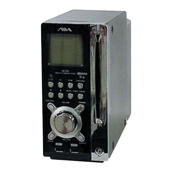
• CX-LZP5 is compact disc receiver
in AWP-ZP5.
AUDIO POWER SPECIFICATIONS
(For the U.S. model)
POWER OUTPUT AND TOTAL HARMONIC
DISTORTION:
With 6-ohm loads, both channels driven, from
120 – 10,000 Hz: rated 20 watts per channel
minimum RMS power, with no more than 10%
total harmonic distortion from 250 milliwatts to
rated output.
Amplifier section
US, CND model:
Continuous RMS power output (reference):
20 + 20 W
(6 ohms at 1 kHz, 10%
THD)
Total harmonic distortion less than 0.9% (6 ohms at
1 kHz, 10 W)
AEP, UK model:
DIN power output (rated):
16 + 16 W
(6 ohms at 1 kHz, DIN)
Continuous RMS power output (reference):
20 + 20 W
(6 ohms at 1 kHz, 10%
THD)
Music power output (reference):
40 + 40 watts (6 ohms at
1 kHz, 10% THD)
Sony Corporation
9-877-863-03
2004K04-1
Personal Audio Company
© 2004. 11
Published by Sony Engineering Corporation
CX-LZP5
Model Name Using Similar Mechanism
CD Mechanism Type
Base Unit Name
Optical Pick-up Name
SPECIFICATIONS
E51, MY, SP, TW model:
The following measured at 110 – 120, 220 – 240 V AC,
50/60 Hz
DIN power output (rated):
Continuous RMS power output (reference):
Inputs
MD (RCA pin jacks):
Outputs
PHONES (stereo mini jack):
SPEAKERS:
USB hub ports
COMPACT DISC RECEIVER
US Model
Canadian Model
AEP Model
UK Model
E Model
CX-LZP3
CDM80BV-F4BD81
BU-F4BD81B
KSM-215CFP
16 + 16 W
(6 ohms at 1 kHz, DIN)
20 + 20 W
(6 ohms at 1 kHz, 10%
THD)
Sensitivity 500 mV,
impedance 47 kilohms
Accepts headphones with
an impedance of 8 ohms or
more
Accepts impedance of
6 ohms
Maximum current
consumption: 100 mA per
port
– Continued on next page –
1
Advertisement
Table of Contents

Related Manuals for Aiwa CX-LZP5


Summary of Contents for Aiwa CX-LZP5
- Page 1 SERVICE MANUAL US Model Canadian Model Ver 1.2 2004. 11 AEP Model UK Model E Model • CX-LZP5 is compact disc receiver in AWP-ZP5. AUDIO POWER SPECIFICATIONS Model Name Using Similar Mechanism CX-LZP3 (For the U.S. model) CD Mechanism Type...
- Page 2 CX-LZP5 Ver 1.2 CD player section Notes on Chip Component Replacement System Compact disc and digital • Never reuse a disconnected chip component. audio system • Notice that the minus side of a tantalum capacitor may be Laser Semiconductor laser damaged by heat.
- Page 3 CX-LZP5 CAUTION Use of controls or adjustments or performance of procedures other than those specified herein may result in hazardous radiation exposure. NOTES ON HANDLING THE OPTICAL PICK-UP BLOCK OR BASE UNIT The laser diode in the optical pick-up block may suffer electrostatic breakdown because of the potential difference generated by the charged electrostatic load, etc.
-
Page 4: Table Of Contents
CX-LZP5 Ver 1.2 TABLE OF CONTENTS 1. SERVICE POSITIONS 6. DIAGRAMS 1-1. CDM Service Position ............5 6-1. IC Pin Description ............. 21 6-2. Block Diagram –CD Section– ........... 26 2. GENERAL 6-3. Block Diagram –Main Section– ........27 6-4. Block Diagram –USB Section– ........28 Main Unit ................ -
Page 5: Service Positions
CX-LZP5 Ver 1.1 SECTION 1 SERVICE POSITIONS 1-1. CDM SERVICE POSITION • The CDM is specified in vertical position and this is the standard position. Check signals such as RF waveform in this position. • Extension of this flexible cable increases workability. -
Page 6: General
CX-LZP5 SECTION 2 GENERAL This section is extracted from instruction manual. List of button locations and reference pages How to use this page Illustration number Use this page to find the location of buttons and other TUNER/BAND 4 6 (13, 15) parts of the system that are mentioned in the text. -
Page 7: Remote Control
CX-LZP5 Remote control ALPHABETICAL ORDER BUTTON DESCRIPTIONS ?/1 (power) 1 (8, 14, 18, 23, A – H I – Z ALBUM +/– 8 (11, 12, 27) i-Bass 8 (17) ./> (go back/go forward) CD qf (10, 12, 14, 15) Number buttons qj (11, 27) -
Page 8: Disassembly
CX-LZP5 SECTION 3 DISASSEMBLY Note : Disassemble the unit in the order as shown below. 3-1. CASE (TOP) (Page 9) 3-2. FRONT PANEL SECTION (Page 9) 3-3. REAR PANEL SECTION, PT SW BOARD (E51 model) (Page 10) 3-4. MAIN BOARD 3-7. -
Page 9: Case (Top)
CX-LZP5 Note : Follow the disassembly procedure in the numerical order given. 3-1. CASE (TOP) 4 case (top) 2 three screws (case 3 TP2 ) 3 two screws (+BVTP 3 x 8) 1 three screws (case 3 TP2 ) 3-2. FRONT PANEL SECTION... -
Page 10: Rear Panel Section, Pt Sw Board (E51, My, Sp Model)
CX-LZP5 Ver 1.2 3-3. REAR PANEL SECTION, PT SW BOARD (E51, MY, SP model) 5 screw 4 screw (+BVTP 3 x 8) (+BVTP 3 x 8) 1 CN451 6 two screws (+BVTP 3 x 8) 2 CN601 7 screw (+BVTP 3 x 8) -
Page 11: Mechanism Deck
CX-LZP5 3-5. MECHANISM DECK 1 screw 2 screw (+BVTP 3 x 8) (+BVTP 3 x 8) 6 two screws (+BVTP 3 x 10) 3 screw (+BVTP 3 x 8) 7 two screws 8 mechanism deck (+BVTP 3 x 10) 4 screw (+BVTP 3 x 8) 3-6. -
Page 12: Usb (A) Board, Usb (B) Board
CX-LZP5 3-7. USB (A) BOARD, USB (B) BOARD 1 CN102 3 two screws (+BVTP 3 x 8) 2 two screws qa three screws (+BVTP 3 x 8) (+BV3 (3-CR) ) qs USB (A) board 5 chassis section chassis (main) 9 screw... -
Page 13: Lever (Loading R/L)
CX-LZP5 3-9. LEVER (LOADING R/L) spr-T (loading-L) spr-T (loading-R) 5 lever (loading-R) 2 two hooks 4 two hooks 3 lever (loading-L) PRECAUTION DURING LEVER (LOADING R / L) INSTALLATION Align the horizontal position. lever (loading-L) lever (loading-R) Install the both levers so that they move symmetrically. -
Page 14: Disc Stop Lever, Disc Sensor Lever
CX-LZP5 3-10. DISC STOP LEVER, DISC SENSOR LEVER 1 gear (cap) 2 gear (IDL-L) PRECAUTION DURING DISC STOP LEVER INSTALLATION chassis (top) hole 5 two hooks 3 two claws disc stop lever 6 disc stop lever hole Install the disc stop lever so that the both holes are aligned. -
Page 15: Cd Board
CX-LZP5 3-12. CD BOARD 4 CD board 3 Remove the two solderings. 2 Remove the two solderings. 1 CN101 3-13. OPTICAL PICK-UP 4 two floating screws 3 two floating screws (+PTPWHM 2.6) (+PTPWHM 2.6) 5 two insulators 6 two insulators... -
Page 16: Base Unit
CX-LZP5 3-14. BASE UNIT 4 floating screw (+PTPWHM 2.6) 6 base unit 3 holder down spring 5 floating screw (+PTPWHM 2.6) 2 lever (CL UP2) 1 screw (+BVTP 2.6 × 8) 3-15. LEVER (BU LOCK) 4 lever (BU lock) 3 three hooks... -
Page 17: Close Lever
CX-LZP5 3-16. CLOSE LEVER 1 washer (3-1-0.4) 5 close lever 3 claw 2 close lever spring 4 shaft disc stop 3-17. DIR LEVER, GEAR (IDL-B) 3 gear pulley capstan retaining ring 4 gear (cap) 5 gear (IDL-A) 8 stopper 9 DIR lever... -
Page 18: Gear (Idl-C)
CX-LZP5 3-18. GEAR (IDL-C) 3 gear (IDL-D) 4 three hooks 2 two claws 1 gear (IDL-F) 5 gear loading lever 7 gear (IDL-C) 6 claw... -
Page 19: Test Mode
CX-LZP5 SECTION 4 TEST MODE [Cold Reset] [Disc Slot Lock] Cold Reset clears all data including the preset data stored in the Disc Slot Lock is an antitheft function to protect demo discs under RAM to initialize the set. Perform this mode when returning the set demonstration in the shop. -
Page 20: Electrical Adjustment
CX-LXP5 SECTION 5 ELECTRICAL ADJUSTMENTS CD SECTION CD section adjustments are done automatically in this set. In case of operation check, confirm that focus bias. FOCUS BIAS CHECK Test Point: 1. Connect the oscilloscope between IC101 pin ra and pin wg (or –... -
Page 21: Diagrams
CX-LZP5 SECTION 6 DIAGRAMS 6-1. IC PIN DESCRIPTION • IC101 CDX3059AR (CD DSP) (CD BOARD) Pin No. Pin Name Pin Description MIRR Mirror signal input/output (Not used) DFCT Defect signal input/output (Not used) Focus OK signal input/output (Not used) —... - Page 22 CX-LZP5 Pin No. Pin Name Pin Description FILO Master PLL (slave = digital PLL) filter output FILI Master PLL filter input Master PLL charge pump output AVDD5 — Analog power supply DDVROUT DC/DC converter output DDVRSEN DC/DC converter output voltage monitor pin AVSS5 —...
- Page 23 CX-LZP5 Pin No. Pin Name Pin Description D ATA Serial data input from CPU — Internal digital ground XLAT Latch input from CPU The serial data is latched at the falling edge CLOCK Serial data transfer clock input from CPU —...
- Page 24 CX-LZP5 • IC700 M3062CMEN-A18FPU0 (SYSTEM CONTROL) (MAIN BOARD) Pin No. Pin Name Pin Description O-LCD DATA LCD data output O-LCD SCK LCD clock output O-LCD CS LCD chip select signal output I-RMC Remocon data input O-MP3 DATA MP3 data output...
- Page 25 CX-LZP5 Pin No. Pin Name Pin Description I-CDM SW1 CD mechanism OUT switch signal input I-CDM SW2 CD mechanism CHUCK switch signal input I-CDM SW3 CD mechanism TRIGGER switch signal input (NCO) — Not used O-MUTE TA mute signal output...
-
Page 26: Block Diagram -Cd Section
CX-LZP5 6-2. BLOCK DIAGRAM — CD SECTION — OPTICAL PICK-UP BLOCK (KSM-215CFP) CD DSP IC101 DETECTOR IC303 MAIN CD-L AOUT1 SECTION +1.5V CD3.3V CD1.5V (Page 27) AOUT2 R-CH XTAII X171 16.9MHz SYSTEM CONTROL XTAO IC700 (1/3) MP3 DECODER CN703 LD POWER... -
Page 27: Block Diagram -Main Section
CX-LZP5 Ver 1.2 6-3. BLOCK DIAGRAM — MAIN SECTION — J603 PHONES J302 IC303 R-CH USB-L SECTION (Page 28) J605 ELECTRONIC VOLUME POWER AMP IC301 IC201 LEVEL IC302 DETECT VOL/TRE/ SPEAKERS CD-L (Page 26) CN601 Q451 MID/BASS SECTION R-CH TUNER-L... -
Page 28: Block Diagram -Usb Section
CX-LZP5 6-4. BLOCK DIAGRAM — USB SECTION — VBUS5V IC804 3.3V VB3.3V USB HUB USB DAC IC802 IC801 POWER J801 CONT VBUS Q801 MAIN SERIAL USB-L DIGITAL SECTION INTERFACE TRANSCEIVER TRANSCEIVER FILTER ENGINE (Page 27) R-CH J802 TRANSCEIVER USB1 VBUS... -
Page 29: Note For Printed Wiring Boards And Schematic Diagrams
CX-LZP5 Ver 1.2 6-5. NOTE FOR PRINTED WIRING BOARDS AND SCHEMATIC DIAGRAMS 6-6. CIRCUIT BOARDS LOCATION THIS NOTE IS COMMON FOR PRINTED WIRING BOARDS AND SCHEMATIC DIAGRAMS. (In addition to this, the necessary note is printed in each block.) for schematic diagram:... -
Page 30: Printed Wiring Board -Cd Section
CX-LZP5 6-8. PRINTED WIRING BOARD — CD SECTION — • Refer to page 29 for Circuit Boards Location. : Uses unleaded solder. M101 IC303 C305 C303 S101 C260 R313 C257 R419 R403 C315 C306 C316 R352 M102 C313 R302 IC251... -
Page 31: Schematic Diagram -Cd Section
CX-LZP5 • Refer to page 29 for Waveforms. 6-9. SCHEMATIC DIAGRAM — CD SECTION — • Refer to page 42 for IC Block Diagrams. TP423 C142 C131 C134 C125 R121 R143 C151 R203 C143 R131 TP424 TP10 C133 TP11 C307... -
Page 32: Schematic Diagram -Main Section (1/2)
CX-LZP5 Ver 1.1 6-10. SCHEMATIC DIAGRAM — MAIN SECTION (1/2) — • Refer to page 43 for IC Block Diagrams. (Page 33) (Page 33) Q455 R461 R462 D454 MC2836 Q456 R464 CN601 C453 R465 R463 EXCEPT AEP,UK R466 Q457 D453... -
Page 33: Schematic Diagram -Main Section (2/2)
CX-LZP5 Ver 1.2 6-11. SCHEMATIC DIAGRAM — MAIN SECTION (2/2) — • Refer to page 29 for Waveforms. R793 CN704 CNA702 R702 R720 R701 R719 R700 R718 D706 Q806 R856 R858 (Page 35) R763 C718 IC703 Q805 R847 R757 C744... -
Page 34: Printed Wiring Boards -Main Section
CX-LZP5 • Semiconductor Ver 1.1 Location Ref. No. Location D001 D002 6-12. PRINTED WIRING BOARDS — MAIN SECTION — • Refer to page 29 for Circuit Boards Location. : Uses unleaded solder. D003 D004 D005 D006 D011 D012 (Page 35) -
Page 35: Printed Wiring Board -Driver Section
CX-LZP5 6-13. PRINTED WIRING BOARD — DRIVER SECTION — 6-14. SCHEMATIC DIAGRAM — DRIVER SECTION — • Refer to page 42 for IC Block Diagram. • Refer to page 29 for Circuit Boards Location. : Uses unleaded solder. IC B/D... -
Page 36: Printed Wiring Board -Usb Section
CX-LZP5 Ver 1.1 6-15. PRINTED WIRING BOARD — USB SECTION — • Refer to page 29 for Circuit Boards Location. : Uses unleaded solder. J811 EP802 • Semiconductor Location Ref. No. Location D801 D802 D803 (Page 34) IC801 IC802 IC804... -
Page 37: Schematic Diagram -Usb Section
CX-LZP5 Ver 1.1 • Refer to page 29 for Waveforms. 6-16. SCHEMATIC DIAGRAM — USB SECTION — • Refer to page 42 for IC Block Diagrams. FB801 L801 R801 Q803 C806 L802 JR823 JR801 Q804 L803 Q801 R804 R803 C805... -
Page 38: Printed Wiring Board -Front Section
CX-LZP5 Ver 1.1 6-17. PRINTED WIRING BOARD — FRONT SECTION — • Refer to page 29 for Circuit Boards Location. : Uses unleaded solder. 1-861-803- (US,CND,AEP,UK) 1-862-657- (E51,MY,SP) (Page 34) • Semiconductor Location Ref. No. Location D901 D902 D903 D906... -
Page 39: Schematic Diagram -Front Section
CX-LZP5 6-18. SCHEMATIC DIAGRAM — FRONT SECTION — C903 C916 CN905 C902 D907 LCD901 D906 (Page 33) IC901 R903 R905 R908 JW921 D902 D901 C901 R904 D903 R902 JW922 C914 Q995 Q994 C915 R911 R913 R916 R924 R928 S930 S941... -
Page 40: Printed Wiring Board -Power Section
CX-LZP5 Ver 1.1 6-19. PRINTED WIRING BOARD — POWER SECTION — • Refer to page 29 for Circuit Boards Location. : Uses unleaded solder. • Semiconductor • Semiconductor EXCEPT E51, MY, SP MODEL Location Location POWER BOARD (EXCEPT E51, MY,... -
Page 41: Schematic Diagram -Power Section
CX-LZP5 Ver 1.1 6-20. SCHEMATIC DIAGRAM — POWER SECTION — EXCEPT E51, MY, SP MODEL CN102 POWER BOARD PT101 CN101 JW102 JW101 PT102 (Page 32) JW104 D102 D103 JW103 R101 C104 C103 3.3M D104 1/2W US,CND MODEL D105 C107 R104... -
Page 42: Ic Block Diagrams
CX-LZP5 6-21. IC BLOCK DIAGRAMS IC251 BA5947FM (CD BOARD) IC301 TC94A34FG-002 (CD BOARD) IC701 BA6956AN (DRIVER BOARD) CH4OUTR CH1PUTF CH1OUTR CH4OUTF LRCKIA CH3OUTF CH2OUTF CONTROL LOGIC PIN26 6.5k CH2OUTR BCKIA CH3OUTR Vref POWVCC POWVCC (ch3, 4) 50k 50k (ch1, 2) - Page 43 CX-LZP5 IC201 STK453-030S (MAIN BOARD (1/2)) STANDBY-BY CIRCUIT PROTECTION CIRCUIT 8 9 10 11 12 13 14 15 16 17 18 IC301 BD3882FV (MAIN BOARD (1/2)) BASS MIDDLE REAR BASS VOLUME REAR VOLUME FRONT TREBLE VOLUME FRONT LOGIC TREBLE MIDDLE...
-
Page 44: Exploded Views
CX-LZP5 Ver 1.2 SECTION 7 EXPLODED VIEWS NOTE: • The mechanical parts with no reference • Color Indication of Appearance Parts The components identified by mark 0 or dotted line with mark number in the exploded views are not supplied. -
Page 45: Front Panel Section
CX-LZP5 Ver 1.2 7-2. FRONT PANEL SECTION not supplied LCD901 not supplied not supplied not supplied (HP board) Ref. No. Part No. Description Remark Ref. No. Part No. Description Remark 4-253-753-01 KNOB (VOL) 4-951-620-01 SCREW (2.6X8), +BVTP 4-253-759-11 PANEL (CD) 3-229-336-11 SCREW, +BVWH TAPPING X-2021-269-1 PANEL ASSY (BLACK)...(BLACK) (E51,MY,SP,TW) -
Page 46: Main Board Section
CX-LZP5 Ver 1.2 7-3. MAIN BOARD SECTION not supplied PT101 not supplied (PT SW board) (E51 model) not supplied not supplied not supplied not supplied not supplied (USB (A) board) not supplied not supplied CDM80BV-F4BD81 not supplied The components identified by Les composants identifiés par une... -
Page 47: Cd Mechanism Deck (1) Section
CX-LZP5 7-4. CD MECHANISM DECK (1) SECTION (CDM80BV-F4BD81) M701 Ref. No. Part No. Description Remark Ref. No. Part No. Description Remark 4-985-672-01 SCREW (+PTPWHM2.6), FLOATING 4-245-630-01 LEVER (SW) 4-249-825-01 SPR-E (HOLDER DOWN) 4-951-620-01 SCREW (2.6X8), +BVTP 4-245-653-01 BELT (MOT) 4-245-639-01 LEVER (CL UP2) -
Page 48: Cd Mechanism Deck (2) Section
CX-LZP5 7-5. CD MECHANISM DECK (2) SECTION (CDM80BV-F4BD81) Ref. No. Part No. Description Remark Ref. No. Part No. Description Remark 4-245-627-01 WASHER (6-2.7-0.4) 4-251-780-01 CAP (CLAMP 215V) 4-245-637-01 ROLLER, RUBBER 4-245-638-01 LEVER (CL UP1) 4-245-649-01 GEAR (IDL-I) 4-985-672-01 SCREW (+PTPWHM2.6), FLOATING... -
Page 49: Cd Mechanism Deck (3) Section
CX-LZP5 7-6. CD MECHANISM DECK (3) SECTION (CDM80BV-F4BD81) supplied supplied supplied Ref. No. Part No. Description Remark Ref. No. Part No. Description Remark 4-245-643-01 GEAR (IDL-C) 4-245-641-01 GEAR (IDL-A) 4-245-644-01 GEAR (IDL-D) 4-245-640-01 GEAR (CAP) 4-248-722-01 SPR-E (DIR) 4-245-628-01 LEVER (BU LOCK) 4-245-642-01 GEAR (IDL-B) 4-248-206-01 WASHER (3-1-0.4) -
Page 50: Base Unit Section
CX-LZP5 7-7. BASE UNIT SECTION S101 The components identified by Les composants identifiés par une mark 0 or dotted line with mark marque 0 sont critiques pour 0 are critical for safety. la sécurité. Replace only with part number Ne les remplacer que par une piéce specified. -
Page 51: Electrical Parts List
CX-LZP5 Ver 1.2 SECTION 8 ELECTRICAL PARTS LIST NOTE: • Due to standardization, replacements in • Items marked “*” are not stocked since The components identified by mark 0 or dotted line with mark the parts list may be different from the they are seldom required for routine service. - Page 52 CX-LZP5 Ver 1.2 DRIVER FRONT Ref. No. Part No. Description Remark Ref. No. Part No. Description Remark < TRANSISTOR > R410 1-216-809-11 METAL CHIP 1/10W R411 1-216-809-11 METAL CHIP 1/10W 6-550-363-01 TRANSISTOR 2SB1690KT146 R412 1-216-809-11 METAL CHIP 1/10W R419 1-216-809-11 METAL CHIP 1/10W <...
- Page 53 CX-LZP5 Ver 1.2 FRONT MAIN Ref. No. Part No. Description Remark Ref. No. Part No. Description Remark D907 6-500-923-01 LED SELU1910CXM (LCD BACK LIGHT) HP BOARD ********* < IC > < CAPACITOR > IC901 6-600-265-01 IC GP1UE28SXK0F (IR) C216 1-162-927-11 CERAMIC CHIP 100PF <...
- Page 54 CX-LZP5 Ver 1.1 MAIN Ref. No. Part No. Description Remark Ref. No. Part No. Description Remark C204 1-126-947-11 ELECT 47uF C340 1-164-227-11 CERAMIC CHIP 0.022uF C207 1-164-156-11 CERAMIC CHIP 0.1uF C341 1-164-227-11 CERAMIC CHIP 0.022uF C208 1-162-968-11 CERAMIC CHIP 0.0047uF 10%...
- Page 55 CX-LZP5 Ver 1.1 MAIN Ref. No. Part No. Description Remark Ref. No. Part No. Description Remark CN601 1-784-737-11 CONNECTOR, FFC 15P (AEP,UK) IC002 6-702-771-01 IC TA78033LS CN700 1-784-778-11 CONNECTOR, FFC 17P IC201 6-600-345-01 IC STK453-030S CN701 1-779-295-11 CONNECTOR, FFC (LIF(NON-ZIF)) 27P...
- Page 56 CX-LZP5 Ver 1.1 MAIN Ref. No. Part No. Description Remark Ref. No. Part No. Description Remark Q456 8-729-120-28 TRANSISTOR 2SC1623-L5L6 R231 1-249-393-11 CARBON 1/4W Q457 8-729-120-28 TRANSISTOR 2SC1623-L5L6 R232 1-249-393-11 CARBON 1/4W 0 R238 Q803 8-729-195-23 TRANSISTOR 2SA952-K2 1-216-361-31 METAL OXIDE 0.22...
- Page 57 CX-LZP5 Ver 1.2 MAIN Ref. No. Part No. Description Remark Ref. No. Part No. Description Remark R362 1-216-825-11 METAL CHIP 2.2K 1/10W R711 1-247-807-31 CARBON 1/4W R363 1-216-841-11 METAL CHIP 1/10W R712 1-247-807-31 CARBON 1/4W R364 1-216-841-11 METAL CHIP 1/10W...
- Page 58 CX-LZP5 Ver 1.2 MAIN POWER PT SW Ref. No. Part No. Description Remark Ref. No. Part No. Description Remark R768 1-247-871-11 CARBON 1/4W 1-861-804-11 POWER BOARD (US,CND,AEP,UK) R769 1-216-821-11 METAL CHIP 1/10W 1-862-658-11 POWER BOARD (E51,MY,SP,TW) R770 1-216-864-11 SHORT CHIP...
- Page 59 CX-LZP5 Ver 1.1 USB (A) USB (B) Ref. No. Part No. Description Remark Ref. No. Part No. Description Remark USB (A) BOARD C848 1-162-919-11 CERAMIC CHIP 22PF C849 1-124-259-11 ELECT 4.7uF ************* C850 1-164-156-11 CERAMIC CHIP 0.1uF < CAPACITOR >...
- Page 60 CX-LZP5 Ver 1.2 USB (B) Ref. No. Part No. Description Remark Ref. No. Part No. Description Remark JR810 1-216-864-11 SHORT CHIP R842 1-216-857-11 METAL CHIP 1/10W JR811 1-216-864-11 SHORT CHIP R843 1-216-818-11 METAL CHIP 1/10W JR812 1-216-864-11 SHORT CHIP R844...
- Page 61 CX-LZP5 Ver 1.2 Ref. No. Part No. Description Remark MISCELLANEOUS *************** 1-828-965-11 WIRE (FLAT TYPE) (11 CORE) (EXCEPT AEP,UK) 1-828-985-11 WIRE (FLAT TYPE) (15 CORE) (AEP,UK) 1-828-991-11 WIRE (FLAT TYPE) (17 CORE) 0 103 1-769-744-52 CORD, POWER (EXCEPT US,CND,TW) 0 103...
- Page 62 CX-LZP5 REVISION HISTORY Clicking the version allows you to jump to the revised page. Also, clicking the version at the upper on the revised page allows you to jump to the next revised page. Ver. Date Description of Revision 2004. 05 2004.