Table of Contents
Advertisement
Quick Links
QQ
3 7 63 1515 0
SERVICE MANUAL
Ver 1.0 2004.05
• CX-BK33 is the amplifier, CD player, tape deck
and tuner section in BMZ-K33.
TE
L 13942296513
Amplifier section
European models:
DIN power output (rated): 100 + 100 W
(6 ohms at 1 kHz, DIN)
Continuous RMS power output (reference):
120 + 120 W
(6 ohms at 1 kHz, 10%
THD)
Music power output (reference):
235 + 235 watts (6 ohms at
1 kHz, 10% THD)
Other models:
The following measured at 120, 220 – 230, 240 V AC,
50/60 Hz
DIN power output (rated): 140 + 140 W
(6 ohms at 1 kHz, DIN)
Continuous RMS power output (reference):
180 + 180 W
(6 ohms at 1 kHz, 10%
THD)
Inputs
MD (AUX) IN L/R (phono jacks):
Sensitivity 1 V,
impedance 47 kilohms
LINE IN AUDIO L/R (phono jacks):
Vo ltage 250 mV,
impedance 47 kilohms
LINE IN VIDEO (phono jack):
1Vp-p, 75 ohms
MIC (phone jack) (Latin American model only):
Sensitivity 1 mV,
www
impedance 10 kilohms
.
Sony Corporation
9-877-873-01
Home Audio Company
2004E05-1
Published by Sony Engineering Corporation
© 2004.05
http://www.xiaoyu163.com
CD Section
TAPE Section
Outputs
PHONES (stereo mini jack):
SPEAKER:
MD (AUX) OUT L/R (phono jacks):
VIDEO OUT (phono jack):
DIGITA L OUT (European and Russian models only):
CD player section
System
Laser
Frequency response
Signal-to-noise ratio
Dynamic range
x
ao
u163
y
i
http://www.xiaoyu163.com
CX-BK33
2 9
8
Model Name Using Similar Mechanism
CD Mechanism Type
Base Unit Name
Optical Pick-up Name
Model Name Using Similar Mechanism
Q Q
Tape Transport Mechanism Type
3
6 7
1 3
1 5
SPECIFICATIONS
Accepts headphones with
an impedance of 32 ohms
or more
Accepts impedance of
6 ohms
Voltage 250 mV,
impedance 1 kilohm
Max. output level 1Vp-p,
unbalanced, Sync
negative, load impedance
75 ohms
Sampling frequencies:
44.1 kHz
Wavelength: 660 nm
Compact disc and digital
audio system
Semiconductor laser
(λ=795 nm)
Emission duration:
continuous
2 Hz – 20 kHz
More than 90 dB
More than 90 dB
COMPACT DISC DECK RECEIVER
co
.
9 4
2 8
AEP Model
UK Model
E Model
NEW
CDM69BV-30CBD64NS
BU-30CBD64NS
A-MAX.3
CX-BK1
CMAL1Z241A
0 5
8
2 9
9 4
2 8
Tape deck section
Recording system
4-track 2-channel stereo
Frequency response
100 – 10,000 Hz, using
Sony TYPE I cassettes
Tuner section
FM stereo, FM/AM superheterodyne tuner
FM tuner section
Tuning range
87.5 – 108.0 MHz
(50-kHz step)
Antenna
FM lead antenna
Antenna terminals
75 ohms unbalanced
Intermediate frequency
10.7 MHz
AM tuner section
Tuning range
European models:
531 – 1,602 kHz
(with the tuning interval
set at 9 kHz)
Other models:
530 – 1,710 kHz
(with the tuning interval
set at 10 kHz)
531 – 1,710 kHz
(with the tuning interval
set at 9 kHz)
Antenna
AM loop antenna, external
antenna terminal
Intermediate frequency
450 kHz
– Continued on next page –
m
9 9
9 9
Advertisement
Table of Contents

Related Manuals for Aiwa CX-BK33


Summary of Contents for Aiwa CX-BK33
- Page 1 3 7 63 1515 0 SERVICE MANUAL AEP Model UK Model Ver 1.0 2004.05 E Model • CX-BK33 is the amplifier, CD player, tape deck and tuner section in BMZ-K33. Model Name Using Similar Mechanism CD Mechanism Type CDM69BV-30CBD64NS CD Section...
- Page 2 CX-BK33 3 7 63 1515 0 General UNLEADED SOLDER Power requirements Boards requiring use of unleaded solder are printed with the lead- European models: free mark (LF) indicating the solder contains no lead. 230 V AC, 50/60 Hz (Caution: Some printed circuit boards may not come printed with Other models: 120, 220 –...
-
Page 3: Playable Discs
CX-BK33 3 7 63 1515 0 Playable discs Notes on CD-R and CD-RW Music discs encoded with copyright protection • Some CD-Rs or CD-RWs cannot be played technologies You can play back the following discs on this on this system depending upon the recording system. -
Page 4: Table Of Contents
CX-BK33 3 7 63 1515 0 TABLE OF CONTENTS SERVICING NOTES 7-16. Printed Wiring Board – FRONT AMP Board – ..... 47 ..........5 7-17. Schematic Diagram – FRONT AMP Board (1/2) – ..48 7-18. Schematic Diagram – FRONT AMP Board (2/2) – ..49 GENERAL 7-19. -
Page 5: Servicing Notes
CX-BK33 SECTION 1 SERVICING NOTES 3 7 63 1515 0 • MODEL IDENTIFICATION NOTES ON HANDLING THE OPTICAL PICK-UP – Rear Cover – BLOCK OR BASE UNIT The laser diode in the optical pick-up block may suffer electrostatic break-down because of the potential difference generated by the charged electrostatic load, etc. - Page 6 CX-BK33 3 7 63 1515 0 – CD mechanism deck – • In checking the CD mechanism deck section, prepare three extension jigs (Part No. J-2501-242-A:1.00 mm 11core/ Part No. J-2501-245-A: 1.00 mm 23 core/Part No. J-2501-248-A: 1.00mm 27 core).
-
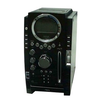
Page 7: General
CX-BK33 SECTION 2 This section is extracted from instruction manual. 3 7 63 1515 0 GENERAL • LOCATION OF CONTROLS Main unit ALPHABETICAL ORDER BUTTON DESCRIPT IONS R – Z ?/1 (power) 1 A – Q REC PAUSE/ START w;... - Page 8 CX-BK33 3 7 63 1515 0 Remote control ALPHABETICAL ORDER BUTTON DESCRIPTIO ?/1 (power) 1 A – E F – Z m/M (rewind/fast forward) ALBUM + qa FM MODE 4 ALBUM – qd FUNCTION +/– 56 X (pause) 8 CD qj PLAY MODE w;...
-
Page 9: Disassembly
CX-BK33 SECTION 3 DISASSEMBLY 3 7 63 1515 0 • This set can be disassembled in the order shown below. 3-1. DISASSEMBLY FLOW Note 1: The process described in can be performed in any order. Note 2: Without completing the process described in , the next process can not be performed. -
Page 10: Side Panel (L)/(R)
CX-BK33 3 7 63 1515 0 Note: Follow the disassembly procedure in the numerical order given. 3-2. SIDE PANEL (L)/(R) 3 side panel (L) 2 screw (BVTP3 × 10) 6 side panel (R) 5 screw (BVTP3 × 10) 1 four screws... -
Page 11: Front Panel Block
CX-BK33 3 7 63 1515 0 3-4. FRONT PANEL BLOCK 1 two wires (flat type) (19 core: CN905, 17 core: CN004) 2 connector (CN602) 6 claw 8 front panel block 4 screw 3 harness (KTP3 × 8) 6 claw 5 screw (BVTP3 ×... -
Page 12: Rear Panel Block
CX-BK33 3 7 63 1515 0 3-6. REAR PANEL BLOCK 2 five screws (BVTP3 × 10) 1 connector (CN303) 3 rear panel block L 13942296513 3-7. TUNER (FM/AM) 2 tuner (FM/AM) 1 two screws (BVTP3 × 6 ) u163... -
Page 13: Speaker Board
CX-BK33 3 7 63 1515 0 3-8. SPEAKER BOARD 1 two screws 2 condenser cover (BVTP3 × 12) 6 SPEAKER board 5 two screws (BVTP3 × 10) 3 connector (CN503) 4 harness 3-9. ACDC BOARD, POWER TRANSFORMER L 13942296513 •... -
Page 14: Front Amp Board Block
CX-BK33 3 7 63 1515 0 3-10. FRONT AMP BOARD BLOCK 3 two screws 2 two screws (BVTP3 × 10) (BVTP3 × 10) 4 FRONT AMP board block 1 two hooks L 13942296513 3-11. CD MECHANISM DECK (CDM69BV-30CBD64NS) 5 two claws... -
Page 15: Base Unit Section (Bu-30Cbd64Ns)
CX-BK33 3 7 63 1515 0 3-12. BASE UNIT SECTION (BU-30CBD64NS) 2 floating screw 4 boss 1 screw (PTPWHM2.6) 6 boss 5 boss 7 base unit section L 13942296513 (BU-30CBD64NS) 3-13. OP ASSY 1 floating screw (PTPWHM2.6) 1 two floating screws 5 OP assy (PTPWHM2.6) -
Page 16: Sw (1) Board, Sw (2) Board, Sw (3) Board, Sw (4) Board, Bracket (Top) Assy
CX-BK33 3 7 63 1515 0 3-14. SW (1) BOARD, SW (2) BOARD, SW (3) BOARD, SW (4) BOARD, BRACKET (TOP) ASSY 4 SW (3) board 5 SW (4) board 3 SW (2) board 1 four screws (BTP2.6 × 6) 6 six screws (BVTP2.6 ×... -
Page 17: Motor (Stocker) Assy (Stocker) (M761)
CX-BK33 3 7 63 1515 0 3-16. MOTOR (STOCKER) ASSY (STOCKER) (M761) 3 two screws (BVTP2.6 × 8) 2 Remove two solders. 5 STOCKER MOTOR board 6 motor (stocker) assy (stocker) (M761) 1 belt (stocker) L 13942296513 3-17. MOTOR (ROLLER) ASSY (ROLLER) (M781) 3 two screws 2 Remove two solders. -
Page 18: Motor (Mode) Assy (Mode) (M771)
CX-BK33 3 7 63 1515 0 3-18. MOTOR (MODE) ASSY (MODE) (M771) 3 two screws (BVTP2.6 × 8) 1 Remove five solders of rotary encoder. 4 MODE MOTOR board 6 motor (mode) assy (mode) (M771) MODE MOTOR board 2 Remove two solders... -
Page 19: Timing Belt (Front/Rear)
CX-BK33 3 7 63 1515 0 3-20. TIMING BELT (FRONT/REAR) 3 slider (mode cam) assy 7 two gears (center) When install three timing belts, its pass under each claws. 8 timing belt (rear) timing belt (rear) 5 two gears... -
Page 20: Sensor Board
CX-BK33 3 7 63 1515 0 3-22. SENSOR BOARD w; harness ql claw q; cam (eject lock) : Note 9 screw (PTPWH2.6 × 8) qj two claws qd gear (eject lock) qk rotary encoder 8 shaft qs cam (BU U/D) -
Page 21: Assembly
CX-BK33 SECTION 4 ASSEMBLY 3 7 63 1515 0 • This set can be assembled in the order shown below. 4-1. HOW TO INSTALL THE CAM (EJECT LOCK) 1 Rotate the cam (BU U/D) fully in the direction of arrow. -
Page 22: How To Install The Gear (Mode 2)
CX-BK33 3 7 63 1515 0 4-3. HOW TO INSTALL THE GEAR (MODE 2) 1 Align the mark on the rotary encoder (S701) with the projection of the assy. 2 Check that the cam (BU U/D) can not be rotated in the direction of arrow. -
Page 23: How To Install The Rotary Encoder (S702), Gear (Stocker Communication)
CX-BK33 3 7 63 1515 0 4-5. HOW TO INSTALL THE ROTARY ENCODER (S702), GEAR (STOCKER COMMUNICATION) 4 gear 5 screw (PTPWH2.6 × 8) (stocker communication) 3 screw 7 two screws (PWH2 × 6) (PTPWH2.6 × 8) 1 rotary encoder... -
Page 24: How To Install The Stocker Assy
CX-BK33 3 7 63 1515 0 4-7. HOW TO INSTALL THE STOCKER ASSY 1 Fit three shafts of the stocker assy in respective slits of the cams (stocker U/D). Note: For the location of slits of the cams (stocker U/D), cam (stocker U/D) see 4-6. -
Page 25: Phase Adjustment Between Pinions (Slider) And Slider-1 To 5 (L/R)
CX-BK33 3 7 63 1515 0 4-8. PHASE ADJUSTMENT BETWEEN PINIONS (SLIDER) AND SLIDER-1 TO 5 (L/R) 1 As shown in the following figure, adjust the portion A of each slider to the boss with the slider-1 to 5 (L) and the slider-1 to 5 (R) pushed in the arrow directions respectively (see Fig. 1). -
Page 26: Test Mode
CX-BK33 SECTION 5 3 7 63 1515 0 TEST MODE 8. Each time the [EQ] knob is pressed, the message “EQ MIN”, COLD RESET “EQ FLAT” or “EQ MAX” is displayed in this order on the The cold reset clears all data including preset data stored in the liquid crystal display. - Page 27 CX-BK33 3 7 63 1515 0 6. Press two buttons of [ENTER] and [EJECT] simultaneously. REPEAT 5 TIMES LIMIT OFF The message “KEYCNT 2” is displayed on the liquid crystal The number of repeat for CD playback is 5 times when the repeat display.
-
Page 28: Electrical Adjustments
CX-BK33 SECTION 6 3 7 63 1515 0 ELECTRICAL ADJUSTMENTS – MAIN Board (Conductor Side) – DECK SECTION 0 dB = 0.775 V • Precaution 1. The adjustment should be performed with the rated power supply voltage. 2. The adjustments should be performed for both L-ch and R-ch. -
Page 29: Cd Section
CX-BK33 3 7 63 1515 0 RFDC signal waveform CD SECTION VOLT/DIV: 200 mV TIME/DIV: 500 ns Note: 1. Use YEDS-18 disc (3-702-101-01) unless otherwise indicated. 2. Use an oscilloscope with more than 10MW impedance. 3. Clean the object lens by an applicator with neutral detergent when the level: 0.6 ±... - Page 30 CX-BK33 3 7 63 1515 0 E-F BALANCE ADJUSTMENT Checking Location: Connection: – BD BOARD (Side B) – oscilloscope BD board TP (TE) TP (VC) – Procedure: 1. Connect an oscilloscpe to test point TP (TE) and TP (VC) on the BD board.
-
Page 31: Diagrams
CX-BK33 SECTION 7 3 7 6 3 1 5 1 5 0 DIAGRAMS 7-1. BLOCK DIAGRAM – CD Section – • R-ch is omitted due to same as L-ch. • SIGNAL PATH OPTICAL PICK-UP : CD PLAY BLOCK DIGITAL SERVO,... -
Page 32: Block Diagram - Tuner/Tape/Usb Section
CX-BK33 7-2. BLOCK DIAGRAM – TUNER/TAPE/USB Section – 3 7 6 3 1 5 1 5 0 (Chilean, Peruvian) MIC LEVEL • R-ch is omitted due to same as L-ch. Q201 • SIGNAL PATH VR201 J201 MIC MIXING : CD PLAY... -
Page 33: Block Diagram - Amp Section
CX-BK33 3 7 6 3 1 5 1 5 0 7-3. BLOCK DIAGRAM – AMP Section – M301 (FAN) SWITCHING Q618 OUTPUT LEVEL DETECT R-CH R-CH Q612, 620, 621 FAN MOTOR DRIVE Q301 – 303 SWITCHING – VH Q619... -
Page 34: Block Diagram - Power Supply Section
CX-BK33 3 7 6 3 1 5 1 5 0 7-4. BLOCK DIAGRAM – POWER SUPPLY Section – – VH POWER, VOLTAGE DC UNBALANCE POWER MONITOR POWER MONITOR AC DETECT (Page 33) DETECT DETECT Q105, 106 Q107 – 109... - Page 35 CX-BK33 3 7 6 3 1 5 1 5 0 • Note for Printed Wiring Boards and Schematic Diagrams • Circuit Boards Location TUNER Note on Printed Wiring Board: Note on Schematic Diagram: • X : parts extracted from the component side.
-
Page 36: Printed Wiring Board - Bd Board
CX-BK33 3 7 6 3 1 5 1 5 0 7-5. PRINTED WIRING BOARDS – BD Board – • See page 35 for Circuit Boards Location. :Uses unleaded solder. • Semiconductor Location Ref. No. Location IC101 IC102 IC103 IC104... -
Page 37: Schematic Diagram - Bd Board
CX-BK33 3 7 6 3 1 5 1 5 0 • See page 66 for IC Block Diagrams. • See page 66 for Waveforms. • See page 72 for IC Pin Function Description. 7-6. SCHEMATIC DIAGRAM – BD Board –... -
Page 38: Printed Wirig Boards - Changer Section
CX-BK33 3 7 6 3 1 5 1 5 0 • See page 35 for Circuit Boards Location. 7-7. PRINTED WIRING BOARDS – CHANGER Section – : Uses unleaded solder. SW (1) BOARD (Page 46) RELAY BOARD (13) SW (2) BOARD... -
Page 39: Schematic Diagram - Changer Section
CX-BK33 • See page 66 for IC Block Diagrams. 7-8. SCHEMATIC DIAGRAM – CHANGER Section – 3 7 6 3 1 5 1 5 0 RELAY BOARD CN751 CN702 R731 DIODE DIODE D SENSE D SENSE R733 CN701 R734 DISC INSERT D+3.3V... -
Page 40: Printed Wiring Board -Deck Board
CX-BK33 3 7 6 3 1 5 1 5 0 • See page 35 for Circuit Boards Location. 7-9. PRINTED WIRING BOARD – DECK Board – : Uses unleaded solder. • Semiconductor Location Ref. No. Location MAIN BOARD D401... -
Page 41: Schematic Diagram - Deck Board
CX-BK33 3 7 6 3 1 5 1 5 0 • See page 66 for Waveforms. 7-10. SCHEMATIC DIAGRAM – DECK Board – R306 JR303 3.9k C309 R307 R321 C317 IC301(1/2) CN008 R376 R317 R315 NJM14558M 1.2k 390k PB-L... -
Page 42: Schematic Diagram - Main Board (1/4)
CX-BK33 3 7 6 3 1 5 1 5 0 • See page 66 for IC Block Diagram. • See page 66 for Waveforms. • See page 72 for IC Pin Function Description. 7-11. SCHEMATIC DIAGRAM – MAIN Board (1/4) –... -
Page 43: Schematic Diagram - Main Board (2/4)
CX-BK33 3 7 6 3 1 5 1 5 0 7-12. SCHEMATIC DIAGRAM – MAIN Section (2/4) – • See page 66 for IC Block Diagrams. (2/4) (AEP,UK) IC604 TOTX141 DIGITAL C668 C669 OPTICAL TRANSCEIVER CD_D-OUT D-GND (Page 42) -
Page 44: Schematic Diagram - Main Board (3/4)
CX-BK33 3 7 6 3 1 5 1 5 0 7-13. SCHEMATIC DIAGRAM – MAIN Section (3/4) – (Page 42) (Page 42) (Page 42) (3/4) (AEP,UK) CN508 RDS DATA RDS INT (AEP,UK) FM SIGNAL OUT C876 C866 C872 C873 +3V(RDS) 0.0033... -
Page 45: Schematic Diagram - Main Board (4/4)
CX-BK33 3 7 6 3 1 5 1 5 0 7-14. SCHEMATIC DIAGRAM – MAIN Section (4/4) – (Page 43) (4/4) (Page 44) CN007 CN507 VSTBY(+9V) ROUT M-GND Q024 2SB1013 A-GND TUNER/AUX GND LOUT (Page 61) R032 RF-GND R020 A-VDD(3.3V) -
Page 46: Printed Wiring Board - Main Board
CX-BK33 • See page 35 for Circuit Boards Location. 7-15. PRINTED WIRING BOARDS – MAIN Section – : Uses unleaded solder. 3 7 6 3 1 5 1 5 0 • Semiconductor Location FM 75Ω (Page 40) (Page 50) FM/AM TUNER Ref. -
Page 47: Printed Wiring Board - Front Amp Board
CX-BK33 3 7 6 3 1 5 1 5 0 • See page 35 for Circuit Boards Location. 7-16. PRINTED WIRING BOARDS – FRONT AMP Board – : Uses unleaded solder. FRONT AMP BOARD R559 C522 C521 R560 Q527... -
Page 48: Schematic Diagram - Front Amp Board (1/2)
CX-BK33 3 7 6 3 1 5 1 5 0 7-17. SCHEMATIC DIAGRAM – FRONT AMP Board (1/2) – (1/2) EP502 R541 D503 2.2k R529 MC2838 R537 4.7k R037 C524 (CHASSIS) 1k 1/2W (E51) 5.6k R543 2.2k 1k 1/4W... -
Page 49: Schematic Diagram - Front Amp Board (2/2)
CX-BK33 3 7 6 3 1 5 1 5 0 7-18. SCHEMATIC DIAGRAM – FRONT AMP Board (2/2) – (Page 48) R695 D629 R681 R686 C636 1SS355TE-17 (2/2) 3.3k 100p 1/2W Q618 1SS355 2SK3053 C637 D623 SWITCHING 1SS355TE-17 R699 3.3k... -
Page 50: Printed Wiring Board - Usb Board
CX-BK33 3 7 6 3 1 5 1 5 0 • See page 35 for Circuit Boards Location. 7-19. PRINTED WIRING BOARD – USB Board – : Uses unleaded solder. • Semiconductor Location Ref. No. Location USB BOARD D700... -
Page 51: Schematic Diagram - Usb Board
CX-BK33 3 7 6 3 1 5 1 5 0 • See page 66 for Waveform. • See page 72 for IC Pin Function Description. 7-20. SCHEMATIC DIAGRAM – USB Board – FB703 FB700 C710 FB701 C717 C719 Q702... -
Page 52: Printed Wiring Board - Mic Board - (Chirean And Peruvian Models)
CX-BK33 3 7 6 3 1 5 1 5 0 • See page 35 for Circuit Boards Location. 7-21. PRINTED WIRING BOARD – MIC Board – (Chirean and Peruvian models) : Uses unleaded solder. MIC BOARD VR201 MAIN BOARD... -
Page 53: Schematic Diagram - Mic Board - (Chirean And Peruvian Models)
CX-BK33 3 7 6 3 1 5 1 5 0 7-22. SCHEMATIC DIAGRAM – MIC Board – (Chirean and Peruvian models) CN205 C217 R208 LCK(NC) I-MIC MIC-OUT R214 C212 MIC-A-GND 0.47 C209 (Page 43) C211 R213 820p R210 2.2k... -
Page 54: Printed Wiring Board - Headphone Board
CX-BK33 3 7 6 3 1 5 1 5 0 • See page 35 for Circuit Boards Location. 7-23. PRINTED WIRING BOARD – HEADPHONE Board – 7-24. SCHEMATIC DIAGRAM – HEADPHONE Board – : Uses unleaded solder. HEADPHONE J521... -
Page 55: Printed Wiring Board - Speaker Board
CX-BK33 3 7 6 3 1 5 1 5 0 • See page 35 for Circuit Boards Location. 7-25. PRINTED WIRING BOARD – SPEAKER Board – 7-26. SCHEMATIC DIAGRAM – SPEAKER Board – :Uses unleaded solder. SPEAKER BOARD CN503... -
Page 56: Printed Wiring Board - Lcd Board
CX-BK33 • See page 35 for Circuit Boards Location. 7-27. PRINTED WIRING BOARD – LCD Board – : Uses unleaded solder. 3 7 6 3 1 5 1 5 0 • Semiconductor Location LCD BOARD Ref. No. Location IC001... -
Page 57: Schematic Diagram - Lcd Board
CX-BK33 3 7 6 3 1 5 1 5 0 • See page 66 for Waveform. 7-28. SCHEMATIC DIAGRAM – LCD Board – JR202 R252 LED266 LED264 Q101 SELU1910CXM SELU1910CXM DTA114EKA-T146 -SLF38 -SLF38 JR205 R251 LED DRIVE LED263 LED261... -
Page 58: Printed Wiring Boards - Key Section
CX-BK33 • See page 35 for Circuit Boards Location. 7-29. PRINTED WIRING BOARDS – KEY Section – :Uses unleaded solder. 3 7 6 3 1 5 1 5 0 POWER KEY BOARD LED302 (STANDBY) R345 S338 R338 ENTER KEY BOARD... -
Page 59: Schematic Diagram - Key Section
CX-BK33 3 7 6 3 1 5 1 5 0 7-30. SCHEMATIC DIAGRAM – KEY Section – CN302 CN005 R327 R328 R329 R330 KEY2 I-RMC KEY2(OUT) S327 S328 S329 S330 KEY2(IN) (Page 57) R310 (Page 57) ENTER TUNER REPEAT/... -
Page 60: Printed Wiring Board - Acdc Board
CX-BK33 • See page 35 for Circuit Boards Location. 7-31. PRINTED WIRING BOARD – ACDC Board – :Uses unleaded solder. 3 7 6 3 1 5 1 5 0 • Semiconductor Location AMP BOARD (Page 47) Ref. No. Location... -
Page 61: Schematic Diagram - Acdc Board
CX-BK33 7-32. SCHEMATIC DIAGRAM – ACDC Board – 3 7 6 3 1 5 1 5 0 CN006 REG-GND(+7V) C008 REG-GND(+4V) JW091 100V REG-GND(+12V) JW090 (Page 49) D004 CN003 D5SBA20 (AEP,UK) D10XB20 (E51) (AEP,UK) CN009 ∗ C016 C015,016 ∗... -
Page 62: Printed Wiring Board - Pt85 Board - (Aep And Uk Models)
CX-BK33 • See page 35 for Circuit Boards Location. 7-33. PRINTED WIRING BOARD – PT85 Board – (AEP and UK models) :Uses unleaded solder. 3 7 6 3 1 5 1 5 0 ACDC BOARD (Page 60) PT85 BOARD CN010 ∗... -
Page 63: Schematic Diagram - Pt85 Board - (Aep And Uk Models)
CX-BK33 3 7 6 3 1 5 1 5 0 7-34. SCHEMATIC DIAGRAM – PT85 Board – (AEP and UK models) PT003 POWER TRANSFORMER (MAIN) CN011 VH(AC) VH(AC) VL(AC) VL(AC) ∗ (Page 61) CN010 (Page 61) C025 0.47 ∗... -
Page 64: Printed Wiring Board - Pt96 Board - (Chirean And Peruvian Models)
CX-BK33 • See page 35 for Circuit Boards Location. 7-35. PRINTED WIRING BOARD – PT96 Board – (Chirean and Peruvian models) :Uses unleaded solder. 3 7 6 3 1 5 1 5 0 ACDC BOARD ACDC BOARD (Page 60) -
Page 65: Schematic Diagram - Pt96 Board - (Chirean And Peruvian Models)
CX-BK33 3 7 6 3 1 5 1 5 0 7-36. SCHEMATIC DIAGRAM – PT96 Board – (Chirean and Peruvian models) PT002 POWER TRANSFORMER (MAIN) CN008 ∗ (Page 61) CN007 CN015 VH(AC) VH(AC) (Page 61) VL(AC) VL(AC) C009 0.47... - Page 66 CX-BK33 3 7 6 3 1 5 1 5 0 • Waveforms • IC Block Diagrams – BD Board – – BD Board – – MAIN Board – IC101 CXD3068Q IC103 qg (RFAC) IC901 qg (X2) (CD Play Mode)
- Page 67 CX-BK33 3 7 63 1515 0 IC102 AN41020A PVCC/2 DIRECTION DETECTION DIRECTION DETECTION DIRECTION DETECTION PVCC/2 DIRECTION DETECTION RESET CIRCUIT . STANDBY . BAND-GAP . SVCC L 13942296513 u163 http://www.xiaoyu163.com...
- Page 68 CX-BK33 3 7 63 1515 0 IC103 CXA2647N-T4 ROM/RW DC OFST RFDCI – – RFDC – ROM/RW VOFST APC AMP RF OFF AT VCC RFAC EQ IN ROM/RW RFAC AC SUM SUMMING VOFST – – ROM/RW TE BAL ROM/RW L 13942296513 –...
- Page 69 CX-BK33 3 7 63 1515 0 IC104 TC94A20F-CX4 Timing SubQ General Generator /RESET Input Port MIMD /MICS /MILP VSSM MIDIO /MICK VDDM /MIACK VDDT L 13942296513 BCKO MP3REQ LRCKO SDIO BCKIA LRCKIA VDDT Switch SDI1 BCKIB u163 http://www.xiaoyu163.com...
- Page 70 CX-BK33 3 7 63 1515 0 – RELAY Board – – MAIN Board – IC701, 711, 721 BA6956AN IC501 BU4052BCF-E2 2XCOM CONTROL LOGIC XCOM IC601 M61529FP-D60G L 13942296513 42 41 39 38 37 34 33 32 31 30 TONE CONTROL...
- Page 71 CX-BK33 3 7 63 1515 0 IC905 MM1614A CURRENT BIAS LIMITTER REFERENCE – DRIVER THERMAL SHUTDOWN L 13942296513 u163 http://www.xiaoyu163.com...
- Page 72 CX-BK33 3 7 63 1515 0 • IC Pin Function Description BD BOARD IC101 CXD3068Q (DIGITAL SERVO, DIGITAL SERVO PROCESSOR) Pin No. Pin Name Description DVDD0 — Power supply terminal (+3.3V) (digital system) XRST Reset signal input from the system controller “L”: reset...
- Page 73 CX-BK33 3 7 63 1515 0 Pin No. Pin Name Description IGEN Stabilized current input for operational amplifiers AVDD0 — Power supply terminal (+3.3V) (analog system) ASYO EFM full-swing output terminal ASYI Asymmetry comparator voltage input terminal RFAC EFM signal input from the RF amplifier AVSS1 —...
- Page 74 CX-BK33 3 7 63 1515 0 MAIN BOARD IC901 uPD703260YGF-S20-JBT-A (SYSTEM CONTROLLER) Pin No. Pin Name Description (ECHO_CE) Tuning signal level input from the RDS decoder (AEP, UK models) I_RDS_SIG Chip enable signal input from the microphone jack (Chilean, Peruvian models)
- Page 75 CX-BK33 3 7 63 1515 0 Pin No. Pin Name Description O-SHIFT_CLK Serial data transfer clock signal output to the shift register O-SHIFT_DATA Serial data output to the shift register O-SHIFT_STB Strobe signal output to the shift register O-PLLCE...
- Page 76 CX-BK33 3 7 63 1515 0 Pin No. Pin Name Description O-SLD_NEG Loading motor control signal output for the CD mechanism O-ELV_NEG Elevator motor control signal output for the CD mechanism I-SLD_E0 SLD_E0 switch signal input from the CD mechanism...
- Page 77 CX-BK33 3 7 63 1515 0 USB BOARD IC700 uAC3553B (USB INTERFACE) Pin No. Pin Name Description System clock input terminal (12MHz) System clock output terminal (12MHz) AREG1 Connected to the external capacitor Ground terminal AVSS_12 — OUTL USB audio signal output terminal (L-ch)
-
Page 78: Q Q 8. 8-1. Panel Section
CX-BK33 SECTION 8 3 7 63 1515 0 EXPLODED VIEWS NOTE: • -XX and -X mean standardized parts, so they • Items marked “*” are not stocked since they The components identified by mark 0 or dotted line with mark 0 are may have some difference from the original are seldom required for routine service. -
Page 79: Tape Mechanism Deck Section (Cmal1Z241A)
CX-BK33 3 7 63 1515 0 8-2. TAPE MECHANISM DECK SECTION (CMAL1Z241A) not supplied not supplied L 13942296513 Ref. No. Part No. Description Remark Ref. No. Part No. Description Remark 4-242-174-01 HLDR, LOCK 1 4-242-171-01 DAMPER 150 N 1-796-351-61 MECHANISM, SINGLE CASSETTE... -
Page 80: Front Boards Section
CX-BK33 3 7 63 1515 0 8-3. FRONT BOARDS SECTION not supplied not supplied (FRONT KEY board) not supplied (POWER KEY board) not supplied (JOG board) not supplied not supplied (ENTER KEY board) supplied (LED board) L 13942296513 supplied... -
Page 81: Front Cabinet Section
CX-BK33 3 7 63 1515 0 8-4. FRONT CABINET SECTION not supplied supplied not supplied supplied L 13942296513 not supplied Ref. No. Part No. Description Remark Ref. No. Part No. Description Remark 4-245-158-01 EMBLEM 4-254-227-01 WINDOW, DISPLAY 4-254-220-11 PANEL, FRONT (E51) X-2021-084-1 KEY ASSY, DISC SELECT (i-BASS. -
Page 82: Main Board Section
CX-BK33 3 7 63 1515 0 8-5. MAIN BOARD SECTION not supplied F001 not supplied L 13942296513 not supplied (SPEAKER board) PT002: E51/ PT003: AEP, UK not supplied (PT85 board: AEP, UK/ PT96 board: E51) chassis section The components identified by mark 0 or dotted line with mark 0 are critical for safety. -
Page 83: Chassis Section
CX-BK33 3 7 63 1515 0 8-6. CHASSIS SECTION not supplied not supplied not supplied supplied L 13942296513 not supplied not supplied CD mechanism deck section-1 (CDM69BV-30CBD64NS) supplied not supplied The components identified by mark 0 or dotted line with mark 0 are critical for safety. -
Page 84: Cd Mechanism Deck Section-1 (Cdm69Bv-30Cbd64Ns)
CX-BK33 3 7 63 1515 0 8-7. CD MECHANISM DECK SECTION-1 (CDM69BV-30CBD64NS) S702 M761 L 13942296513 not supplied (ST encorder board) CD mechanism deck section-2 Ref. No. Part No. Description Remark Ref. No. Part No. Description Remark 1-686-725-13 STOCKER MOTOR BOARD 4-239-689-01 GEAR (STOCKER DECELERATION) 4-951-620-01 SCREW (2.6X8), +BVTP... -
Page 85: Cd Mechanism Deck Section-2 (Cdm69Bv-30Cbd64Ns)
CX-BK33 3 7 63 1515 0 8-8. CD MECHANISM DECK SECTION-2 (CDM69BV-30CBD64NS) CD mechanism deck section-3 L 13942296513 CD mechanism deck section-5 base unit section (BU-30CBD64NS) Ref. No. Part No. Description Remark Ref. No. Part No. Description Remark 1-686-727-13 SW BOARD (1) -
Page 86: Cd Mechanism Deck Section-3 (Cdm69Bv-30Cbd64Ns)
CX-BK33 3 7 63 1515 0 8-9. CD MECHANISM DECK SECTION-3 (CDM69BV-30CBD64NS) not supplied supplied not supplied supplied supplied L 13942296513 not supplied Ref. No. Part No. Description Remark Ref. No. Part No. Description Remark X-4955-447-1 PULLEY (A) (BU30) ASSY 4-240-039-01 LEVER (DISC STOPPER) 4-992-069-01 SCREW (+PTPWH) (M2) (DIA. -
Page 87: Cd Mechanism Deck Section-4 (Cdm69Bv-30Cbd64Ns)
CX-BK33 3 7 63 1515 0 8-10. CD MECHANISM DECK SECTION-4 (CDM69BV-30CBD64NS) supplied L 13942296513 M781 CD mechanism deck section-5 Ref. No. Part No. Description Remark Ref. No. Part No. Description Remark X-4954-626-1 LEVER (ROLLER) ASSY 4-240-041-01 SPRING (SLIDER 2), TENSION 4-239-666-01 GEAR 4-951-620-01 SCREW (2.6X8), +BVTP... -
Page 88: Cd Mechanism Deck Section-5 (Cdm69Bv-30Cbd64Ns)
CX-BK33 3 7 63 1515 0 8-11. CD MECHANISM DECK SECTION-5 (CDM69BV-30CBD64NS) L 13942296513 CD mechanism deck section-6 Ref. No. Part No. Description Remark Ref. No. Part No. Description Remark 4-240-020-01 GEAR (TIMING) 4-239-699-01 PULLEY u163 4-239-708-02 BELT (FRONT), TIMING... -
Page 89: Cd Mechanism Deck Section-6 (Cdm69Bv-30Cbd64Ns)
CX-BK33 3 7 63 1515 0 8-12. CD MECHANISM DECK SECTION-6 (CDM69BV-30CBD64NS) M771 not supplied L 13942296513 supplied S771 Ref. No. Part No. Description Remark Ref. No. Part No. Description Remark 4-239-693-02 CAM (GEAR) 4-239-692-02 CAM (BU U/D) 1-686-723-13 SENSOR BOARD... -
Page 90: Base Unit Section (Bu-30Cbd64Ns)
CX-BK33 3 7 63 1515 0 8-13. BASE UNIT SECTION (BU-30CBD64NS) not supplied M101 (spindle) not supplied M102 (sled) L 13942296513 The components identified by mark 0 or dotted line with mark 0 are critical for safety. Replace only with part number specified. -
Page 91: Electrical Parts List
CX-BK33 SECTION 9 ELECTRICAL PARTS LIST 3 7 63 1515 0 ACDC NOTE: • Due to standardization, replacements in the • Items marked “*” are not stocked since they The components identified by mark 0 or dotted line with mark 0 are parts list may be different from the parts are seldom required for routine service. - Page 92 CX-BK33 3 7 63 1515 0 ACDC Ref. No. Part No. Description Remark Ref. No. Part No. Description Remark Q107 8-729-120-28 TRANSISTOR 2SC1623-L5L6 A-4731-674-A BD BOARD, COMPLETE Q108 8-729-120-28 TRANSISTOR 2SC1623-L5L6 ******************* Q109 8-729-120-28 TRANSISTOR 2SC1623-L5L6 Q110 6-550-580-01 TRANSISTOR 2SA1235TP-1F <...
- Page 93 CX-BK33 3 7 63 1515 0 Ref. No. Part No. Description Remark Ref. No. Part No. Description Remark C259 1-164-360-11 CERAMIC CHIP 0.1uF R103 1-216-845-11 METAL CHIP 100K 1/10W R104 1-216-835-11 METAL CHIP 1/10W C260 1-128-590-11 ELECT CHIP 100uF 6.3V...
- Page 94 CX-BK33 3 7 63 1515 0 DECK Ref. No. Part No. Description Remark Ref. No. Part No. Description Remark C401 1-126-956-11 ELECT 0.1uF R260 1-216-821-11 METAL CHIP 1/10W C402 1-126-956-11 ELECT 0.1uF R261 1-164-360-11 CERAMIC CHIP 0.1uF C403 1-162-926-11 CERAMIC CHIP...
- Page 95 CX-BK33 3 7 63 1515 0 DECK ENTER KEY FRONT AMP Ref. No. Part No. Description Remark Ref. No. Part No. Description Remark R419 1-216-821-11 METAL CHIP 1/10W < COIL > R420 1-216-821-11 METAL CHIP 1/10W L451 1-456-094-11 TRANSFORMER, BIAS OSCILLATION...
- Page 96 CX-BK33 FRONT AMP 3 7 63 1515 0 Ref. No. Part No. Description Remark Ref. No. Part No. Description Remark C501 1-162-970-11 CERAMIC CHIP 0.01uF D619 6-500-334-01 DIODE MC2836 C502 1-162-970-11 CERAMIC CHIP 0.01uF D623 8-719-988-61 DIODE 1SS355TE-17 D624...
- Page 97 CX-BK33 3 7 63 1515 0 FRONT AMP Ref. No. Part No. Description Remark Ref. No. Part No. Description Remark Q524 8-729-120-28 TRANSISTOR 2SC1623-L5L6 R515 1-216-033-00 RES-CHIP 1/10W Q525 8-729-052-79 TRANSISTOR 2SD1306NETL R516 1-216-033-00 RES-CHIP 1/10W Q526 8-729-052-79 TRANSISTOR...
- Page 98 CX-BK33 FRONT AMP 3 7 63 1515 0 FRONT KEY Ref. No. Part No. Description Remark Ref. No. Part No. Description Remark R574 1-216-009-00 RES-CHIP 1/10W R575 1-216-833-11 METAL CHIP 1/10W R692 1-249-423-11 CARBON 3.3K 1/4W R576 1-216-833-11 METAL CHIP...
- Page 99 CX-BK33 3 7 63 1515 0 FRONT KEY HEADPHONE Ref. No. Part No. Description Remark Ref. No. Part No. Description Remark S322 1-771-410-21 SWITCH, TACTILE (ALBUM –) S323 1-771-410-21 SWITCH, TACTILE (ALBUM +) C110 1-164-360-11 CERAMIC CHIP 0.1uF S324...
- Page 100 CX-BK33 3 7 63 1515 0 MAIN Ref. No. Part No. Description Remark Ref. No. Part No. Description Remark LED258 8-719-061-96 LED SLR-325DCT31 (DISC INDICATOR 4) R602 1-216-833-11 METAL CHIP 1/10W R603 1-216-833-11 METAL CHIP 1/10W LED259 8-719-061-96 LED SLR-325DCT31 (DISC INDICATOR 5)
- Page 101 CX-BK33 3 7 63 1515 0 MAIN Ref. No. Part No. Description Remark Ref. No. Part No. Description Remark C521 1-162-927-11 CERAMIC CHIP 100PF C655 1-164-388-11 CERAMIC CHIP 270PF (AEP, UK) C656 1-107-826-11 CERAMIC CHIP 0.1uF C657 1-119-774-11 ELECT...
- Page 102 CX-BK33 MAIN 3 7 63 1515 0 Ref. No. Part No. Description Remark Ref. No. Part No. Description Remark C867 1-162-970-11 CERAMIC CHIP 0.01uF C959 1-162-964-11 CERAMIC CHIP 0.001uF (AEP, UK) C960 1-162-964-11 CERAMIC CHIP 0.001uF C961 1-162-964-11 CERAMIC CHIP 0.001uF...
- Page 103 CX-BK33 3 7 63 1515 0 MAIN Ref. No. Part No. Description Remark Ref. No. Part No. Description Remark JK603 1-774-227-11 JACK, PIN 1P (VIDEO OUT) R011 1-216-134-00 RES-CHIP 1/8W R016 1-249-413-11 CARBON 1/4W < SHORT > R017 1-216-841-11 METAL CHIP...
- Page 104 CX-BK33 MAIN 3 7 63 1515 0 R729 1-216-833-11 METAL CHIP 1/10W R627 1-216-829-11 METAL CHIP 4.7K 1/10W R730 1-216-821-11 METAL CHIP 1/10W (E51) R731 1-216-825-11 METAL CHIP 2.2K 1/10W R628 1-216-829-11 METAL CHIP 4.7K 1/10W R732 1-216-825-11 METAL CHIP 2.2K...
- Page 105 CX-BK33 3 7 63 1515 0 MAIN Ref. No. Part No. Description Remark Ref. No. Part No. Description Remark R895 1-216-825-11 METAL CHIP 2.2K 1/10W R958 1-216-840-11 METAL CHIP 1/10W R896 1-216-826-11 METAL CHIP 2.7K 1/10W R959 1-216-823-11 METAL CHIP 1.5K...
- Page 106 CX-BK33 MODE MOTOR 3 7 63 1515 0 POWER KEY PT85 PT96 RELAY Ref. No. Part No. Description Remark Ref. No. Part No. Description Remark POWER KEY BOARD < CONNECTOR > **************** CN205 1-784-766-11 CONNECTOR, FFC 5P < LED >...
- Page 107 CX-BK33 RELAY ROLLER MOTOR SENSOR 3 7 63 1515 0 SPEAKER ST ENCODER STOCKER MOTOR SW (1) SW (2) Ref. No. Part No. Description Remark Ref. No. Part No. Description Remark C762 1-164-159-21 CERAMIC 0.1uF SPEAKER BOARD ************** C763 1-164-159-21 CERAMIC 0.1uF...
- Page 108 CX-BK33 SW (3) 3 7 63 1515 0 SW (4) Ref. No. Part No. Description Remark Ref. No. Part No. Description Remark 1-686-729-13 SW (3) BOARD < DIODE > ************ D700 8-719-988-61 DIODE 1SS355TE-17 < SWITCH > D701 8-719-988-61 DIODE 1SS355TE-17...
- Page 109 CX-BK33 3 7 63 1515 0 Ref. No. Part No. Description Remark Ref. No. Part No. Description Remark R705 1-216-832-11 METAL CHIP 8.2K 1/10W ACCESSORIES R706 1-216-835-11 METAL CHIP 1/10W *********** R707 1-216-835-11 METAL CHIP 1/10W R710 1-216-849-11 METAL CHIP...
- Page 110 CX-BK33 3 7 63 1515 0 REVISION HISTORY Clicking the version allows you to jump to the revised page. Also, clicking the version at the upper right on the revised page allows you to jump to the next revised page.
Need help?
Do you have a question about the CX-BK33 and is the answer not in the manual?
Questions and answers