Table of Contents
Advertisement
Quick Links
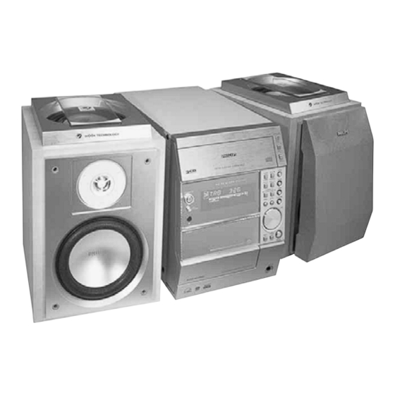
Micro System
Service
Service
Service
Service Manual
©
Copyright 2001 Philips Consumer Electronics B.V. Eindhoven, The Netherlands
All rights reserved. No part of this publication may be reproduced, stored in a retrieval system or
transmitted, in any form or by any means, electronic, mechanical, photocopying, or otherwise
without the prior permission of Philips.
Published by KC 0110 Service Audio
TABLE OF CONTENTS
Location Of Pc Boards & Version variations ................ 1-2
Technical Specifications ............................................. 1-3
Measurement Setup .................................................... 1-4
Service Aids, Safety Instruction, etc. .......................... 1-5
Instruction for use: European version excerpt .......... 2-1
Additional features .................. 2-13
Disassembly Instructions & Service positions ........... 3-1
Service Test Programs ............................................... 3-4
Set Block Diagram ......................................................... 4
Set Wiring Diagram ........................................................ 5
Front Display Board ....................................................... 6
Eco6 Tuner Board: System Non-Cenelec ................ 7A
System Cenelec ........................ 7B
Front Control Board ....................................................... 8
Etf6-Le Tape Module ................................................... 9
3TDC Module ............................................................... 10
Power 2001 Module ..................................................... 11
Set Mechanical Exploded view & parts list ................. 12
Printed in The Netherlands
Subject to modification
MC-70/
Page
Class 1
GB
21/21M/22/37
COMPACT
DIGITAL AUDIO
3139 785 22720
Advertisement
Table of Contents


Need help?
Do you have a question about the MC-70 and is the answer not in the manual?
Questions and answers