Table of Contents
Advertisement
HCD-MX500i/MX550i
SERVICE MANUAL
Ver. 1.0 2010.05
• HCD-MX500i is the amplifi er, CD player, tuner, USB (Except Canadian) and iPod/iPhone section in CMT-MX500i.
• HCD-MX550i is the amplifi er, CD player, tuner, USB and iPod/iPhone section in CMT-MX550i.
•
iPod is a trademark of Apple Inc.
•
iPhone is a trademark of Apple Inc.
•
MPEG Layer-3 audio coding technology and patents licensed from Fraunhofer IIS and Thomson.
•
Windows Media is either a registered trademark or trademark of Microsoft Corporation in the
United States and/or other countries.
•
This product is protected by certain intellectual property rights of Microsoft Corporation. Use or
distribution of such technology outside of this product is prohibited without a license from Micro-
soft or an authorized Microsoft subsidiary.
•
All other trademarks and registered trademarks are of their respective holders. In this manual, ™
and ® marks are not specifi ed.
Main unit
AUDIO POWER SPECIFICATIONS
With 6 ohm loads, both channels driven, from 120
10,000 Hz; rated 30 watts
per channel minimum RMS power, with no more than 10% total harmonic
distortion from 250 milliwatts to rated output.
Amplifier section
European model:
DIN power output (rated): 25 watts + 25 watts (6 ohms at 1 kHz, DIN)
Continuous RMS power output (reference): 30 watts + 30 watts (6 ohms at
1 kHz, 10% THD)
Music power output (reference): 30 watts + 30 watts (6 ohms at 1 kHz, 10%
THD)
Other models:
DIN power output (rated): 25 watts + 25 watts (6 ohms at 1 kHz, DIN)
Continuous RMS power output (reference): 30 watts + 30 watts (6 ohms at
1 kHz, 10% THD)
Input
AUDIO IN (stereo mini jack): Sensitivity 700 mV, impedance 47 kilohms
Outputs
SPEAKERS: Accepts impedance of 6 ohms
CD player section
System: Compact disc and digital audio system
Laser Diode Properties
Emission Duration: Continuous
Laser Output*: Less than 44.6μW
* This output is the value measurement at a distance of 200mm from the
objective lens surface on the Optical Pick-up Block with 7mm aperture.
Frequency response: 20 Hz
20 kHz
Signal-to-noise ratio: More than 90 dB
Dynamic range: More than 90 dB
Tuner section
FM tuner section:
FM stereo, FM superheterodyne tuner
Tuning range:
North American model: 87.5 MHz
108.0 MHz (100 kHz step)
Other models: 87.5 MHz
108.0 MHz (50 kHz step)
Antenna: FM lead antenna
Antenna terminals: 75 ohms unbalanced
Intermediate frequency: 10.7 MHz
DAB/DAB+ tuner section (MX550i only):
FM stereo, DAB/FM superheterodyne tuner
Frequency range*
Band-III: 174.928 (5A) MHz
239.200 (13F) MHz
* For details, see "DAB/DAB+ frequency table" below.
Antenna: DAB/FM lead antenna
Antenna terminal: 75 ohms, F female
Sony Corporation
9-889-872-01
2010E05-1
Audio&Video Business Group
©
2010.05
Published by Sony Techno Create Corporation
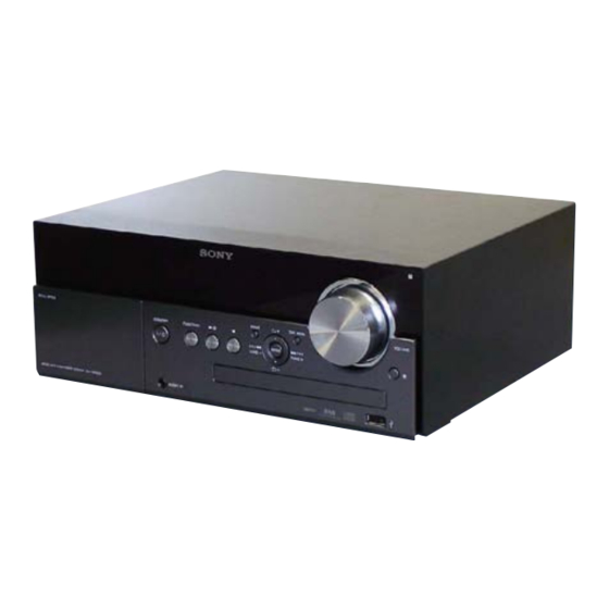
Photo: HCD-MX550i
Model Name Using Similar Mechanism
CD Mechanism Type
Optical Pick-up Block Name
SPECIFICATIONS
DAB/DAB+ frequency table (Band-III)
Frequency
Label
Frequency
174.928 MHz
5A
209.936 MHz
176.640 MHz
5B
211.648 MHz
178.352 MHz
5C
213.360 MHz
180.064 MHz
5D
215.072 MHz
181.936 MHz
6A
216.928 MHz
183.648 MHz
6B
218.640 MHz
185.360 MHz
6C
220.352 MHz
187.072 MHz
6D
222.064 MHz
188.928 MHz
7A
223.936 MHz
190.640 MHz
7B
225.648 MHz
192.352 MHz
7C
227.360 MHz
194.064 MHz
7D
229.072 MHz
195.936 MHz
8A
230.784 MHz
197.648 MHz
8B
232.496 MHz
199.360 MHz
8C
234.208 MHz
201.072 MHz
8D
235.776 MHz
202.928 MHz
9A
237.488 MHz
204.640 MHz
9B
239.200 MHz
206.352 MHz
9C
208.064 MHz
9D
* Frequencies are displayed to two decimal places on this system.
Canadian Model
Chinese Model
Singapore Model
iPod/iPhone section
Compatible iPod/iPhone models:
Label
iPod touch 2nd generation
10A
iPod touch 1st generation
iPod classic 120 GB, 160 GB (2009)
10B
iPod classic 160 GB (2007)
10C
iPod classic 80 GB
10D
iPod nano 5th generation (video camera)
iPod nano 4th generation (video)
11A
iPod nano 3rd generation (video)
11B
iPod nano 2nd generation (aluminum)
11C
iPod nano 1st generation
11D
iPod 5th generation (video)
iPod 4th generation (color display)
12A
iPod 4th generation
12B
iPod mini
12C
iPhone
iPhone 3G
12D
iPhone 3GS
13A
USB section (except for North American model)
13B
Supported bit rate:
13C
MP3 (MPEG 1 Audio Layer-3): 32 kbps
WMA: 48 kbps
192 kbps, VBR
13D
AAC: 48 kbps
320 kbps
13E
Sampling frequencies:
MP3 (MPEG 1 Audio Layer-3): 32/44.1/48 kHz
13F
WMA: 44.1 kHz
AAC: 44.1 kHz
(USB) port: Type A, maximum current 500 mA
General
Power requirements:
North American model: AC 120 V, 60 Hz
Other models: AC 220 V
240 V, 50/60 Hz
Power consumption: 33 watts
Dimensions (W/H/D) (excl. speakers):
Approx. 309 mm × 122 mm × 247 mm
Mass (excl. speakers): Approx. 2.9 kg
Design and specifications are subject to change without notice.
Standby power consumption: 0.5 W
Halogenated flame retardants are not used in the certain printed
wiring boards.
COMPACT DISC RECEIVER
HCD-MX500i
AEP Model
HCD-MX500i/MX550i
UK Model
HCD-MX550i
NEW
CDM85CD-DVBU102
KHM-313CAA
320 kbps, VBR
Advertisement
Table of Contents

Related Manuals for Sony HCD-MX500i


Summary of Contents for Sony HCD-MX500i
-
Page 1: Specifications
UK Model HCD-MX550i Photo: HCD-MX550i • HCD-MX500i is the amplifi er, CD player, tuner, USB (Except Canadian) and iPod/iPhone section in CMT-MX500i. • HCD-MX550i is the amplifi er, CD player, tuner, USB and iPod/iPhone section in CMT-MX550i. • iPod is a trademark of Apple Inc. -
Page 2: Table Of Contents
6-6. CD Mechanism Deck Section PIÈCES SONT CRITIQUES POUR LA SÉCURITÉ DE FONC- (CDM85CD-DVBU102) ..........59 TIONNEMENT. NE REMPLACER CES COMPOSANTS QUE PAR DES PIÈCES SONY DONT LES NUMÉROS SONT DON- ELECTRICAL PARTS LIST ......60 NÉS DANS CE MANUEL OU DANS LES SUPPLÉMENTS... -
Page 3: Servicing Notes
The laser beam on this model is concentrated so as to be focused Model Part No. on the disc refl ective surface by the objective lens in the optical HCD-MX500i: AEP model 4-175-955-0[] pickup block. Therefore, when checking the laser diode emission, HCD-MX500i: Canadian model 4-175-955-2[] observe from more than 30 cm away from the objective lens. - Page 4 HCD-MX500i/MX550i CAPACITOR ELECTRICAL DISCHARGE PROCESSING When checking the board, the electrical discharge is necessary for the electric shock prevention. Connect the resistors referring to the fi gure below. • POWER board (C11, C12) (Canadian model) Both ends of respective capacitors.
- Page 5 HCD-MX500i/MX550i HOW TO OPEN THE TRAY WHEN POWER SWITCH TURN OFF bottom side 1 Insert the hard metal fittings of L character type in the hole of the chassis, and push the lever in the direction of the arrow. MAIN, BD96/BD96U AND SP BOARDS SERVICE POSITION...
- Page 6 HCD-MX500i/MX550i FL, KEY, JACK AND USB BOARDS SERVICE POSITION JACK board MAIN board KEY board FL board BD96 board (Canadian) BD96U board (Except Canadian) USB board (Except Canadian) CD MECHANISM DECK, MAIN AND BD96/BD96U BOARDS SERVICE POSITION MAIN board BD96 board (Canadian)
- Page 7 HCD-MX500i/MX550i POWER BOARD SERVICE POSITION POWER board MAIN board FL board...
-
Page 8: Disassembly
HCD-MX500i/MX550i SECTION 2 DISASSEMBLY • This set can be disassembled in the order shown below. 2-1. DISASSEMBLY FLOW 2-2. CASE (Page 8) 2-3. FRONT PANEL BLOCK 2-5. MAIN BOARD 2-6. SP BOARD (Page 9) (Page10) (Page 11) 2-4. KNOB (VOL) 2-8. -
Page 9: Front Panel Block
HCD-MX500i/MX550i 2-3. FRONT PANEL BLOCK qd screw (BV3) qf lead wire (from HP board) 7 ferrite core 5 Lift up the coating clip. 9 connector (CN402) 8 flexible flat cable qs two screws (13 core) (CN404) (BV3) 6 flexible flat cable... -
Page 10: Knob (Vol)
HCD-MX500i/MX550i 2-4. KNOB (VOL) Note: The illustration sees the front panel block from FL board side. FL board 2 knob (VOL) front panel block hole 1 Push the knob (VOL) by flat-head screwdriver. 2-5. MAIN BOARD qg two screws (BV3) -
Page 11: Sp Board
HCD-MX500i/MX550i 2-6. SP BOARD 2 connector (CN703) 1 connector (CN702) 6 SP board 5 clamp filter 3 screw (BV3) 2-7. POWER BOARD 6 two screws (BV3) 2 two screws (BV3) 6 two screws (BV3) 7 POWER board 6 two screws (BV3) -
Page 12: Cd Block
HCD-MX500i/MX550i 2-8. CD BLOCK 2 four screws (BV3) Note 1: Do not remove this connector (CN201) at this point. It is necessary to process electrostatic measures of optical pick-up. 1 connector (CN301) bracket (front) 7 two claws 6 bracket (center) -
Page 13: Bd96/Bd96U Board
HCD-MX500i/MX550i 2-9. BD96/BD96U BOARD Note 1: When disconnection the wire (fl at type) (24 core) of optical pick-up block, solder the short-land. 1 Solder the short-land. 2 wire (flat type) (24 core) (CN201) Note 2: When assembling the optical pick-up block, remove the solder of short-land after connecting the wire (flat type) (24 core). -
Page 14: Ffc Holder
HCD-MX500i/MX550i 2-11. FFC HOLDER Note 1: The illustration sees the CD mechanism deck block from optical pick-up block side. 3 FFC holder Note 2: Remove the FFC holder from the 2 two claws original set and install it again. 1 two claws... -
Page 15: Test Mode
HCD-MX500i/MX550i SECTION 3 TEST MODE COLD RESET 8. Press the [TOOL MENU] button, the key test mode is acti- vated and “K 0 V0” is displayed on the fl uorescent indicator The cold reset clears all data including preset data stored in the tube. - Page 16 HCD-MX500i/MX550i CD SERVICE MODE Use this key to execute Command Out in the Command Out Mode. This mode can run the CD sled motor freely. Use this mode, for instance, when cleaning the optical pick-up. CD Servo Test Mode Tree:...
- Page 17 HCD-MX500i/MX550i CD ERROR CODE 08: The disc chucking-release completion operation is in prog- ress. The past errors of the CD mechanism (CDM) are displayed as the CDM Errors, and those of the optical pick-up system (= optical 4 It indicates the operation during which the trouble has oc- unit + BD96/BD96U board) are displayed as the BD Errors as curred.
-
Page 18: Electrical Check
HCD-MX500i/MX550i SECTION 4 ELECTRICAL CHECK FM TUNE LEVEL CHECK signal generator Procedure: 1. Turn on the set. 2. Input the following signal from signal generator to FM antenna input directly. Carrier frequency : A = 87.5 MHz, B = 98 MHz, C = 108 MHz... -
Page 19: Diagrams
HCD-MX500i/MX550i SECTION 5 DIAGRAMS 5-1. BLOCK DIAGRAM - CD, USB Section - O OFF (Page 20) 6 9 4 9 FOO HCD-MX500i/MX550i... -
Page 20: Block Diagram - Tuner, Ipod/Iphone, Audio In Section
HCD-MX500i/MX550i 5-2. BLOCK DIAGRAM - TUNER, iPod/iPhone, AUDIO IN Section - (Page 19) CD-L 1 IN-L2 ELECTRICAL VOLUME, INPUT SELECTOR IC502 (MX550i) 7 IN-L5 SEL L VOL L OUT L SP_L (Page 21) SB L IN-L4 R-CH J302 IN-L1 AUDIO IN... -
Page 21: Block Diagram - Output, Panel Section
HCD-MX500i/MX550i 5-3. BLOCK DIAGRAM - OUTPUT, PANEL Section - A/D CONVERTER STREAM PROCESSOR DIGITAL POWER AMP IC711 IC705 IC707 TB322 SP-L 2 AINL SDTO 9 31 DATA OUTL1 6 PWM_A OUT_A – (Page 20) OUTL2 PWM_B OUT_B R-CH 1 AINR... -
Page 22: Block Diagram - Power Supply Section
HCD-MX500i/MX550i 5-4. BLOCK DIAGRAM - POWER SUPPLY Section - (Except Canadian) VBUS +5V REGULATOR IC506 iPod +5V REGULATOR IC510 +3.3V A/D +3.3V REGULATOR IC702 +3.3V CD A +3.3V REGULATOR IC505 CD +5V REGULATOR IC504 M +7V REGULATOR T031 IC904 MAIN POWER... - Page 23 HCD-MX500i/MX550i THIS NOTE IS COMMON FOR PRINTED WIRING BOARDS AND SCHEMATIC DIAGRAMS. • Circuit Boards Location. (In addition to this, the necessary note is printed in each block.) For Printed Wiring Boards. For Schematic Diagrams. Note: Note: • X : Parts extracted from the component side.
-
Page 24: Printed Wiring Board - Bd96/Bd96U Board (Side A)
HCD-MX500i/MX550i 5-5. PRINTED WIRING BOARD - BD96/BD96U Board (Side A) - • See page 23 for Circuit Boards Location. • : Uses unleaded solder. (SPINDLE) (SLED) OPTICAL (LIMIT) BD96 BOARD PICK-UP (CND) BLOCK (Page 31) (KHM-313CAA) BD96U BOARD MAIN BOARD... -
Page 25: Printed Wiring Board - Bd96/Bd96U Board (Side B)
HCD-MX500i/MX550i 5-6. PRINTED WIRING BOARD - BD96/BD96U Board (Side B) - • See page 23 for Circuit Boards Location. • : Uses unleaded solder. BD96 BOARD (CND) BD96U BOARD (EXCEPT CND) (SIDE B) R306 R316 (EXCEPT CND) X401 R221 R214... -
Page 26: Schematic Diagram - Bd96/Bd96U Board (1/2)
HCD-MX500i/MX550i 5-7. SCHEMATIC DIAGRAM - BD96/BD96U Board (1/2) - • See page 28 for Waveforms. • See page 42 for IC Block Diagrams. • See page 47 for IC Pin Function Description. BD96 BOARD (1/2) (CND) BD96U BOARD (1/2) C208... -
Page 27: Schematic Diagram - Bd96/Bd96U Board (2/2)
HCD-MX500i/MX550i 5-8. SCHEMATIC DIAGRAM - BD96/BD96U Board (2/2) - See page 28 for Waveforms. • • See page 42 for IC Block Diagrams. • See page 47 for IC Pin Function Description. BD96 BOARD (2/2) (CND) BD96U BOARD (2/2) BD96/BD96U... -
Page 28: Printed Wiring Board - Dab Board (Mx550I)
HCD-MX500i/MX550i • Waveforms 5-9. PRINTED WIRING BOARD - DAB Board (MX550i) - • See page 23 for Circuit Boards Location. • : Uses unleaded solder. – BD96/BD96U Board – – MAIN Board – IC101 wf (XO) IC401 qa (Xcout) (CD play mode) -
Page 29: Schematic Diagram - Dab Board (Mx550I)
HCD-MX500i/MX550i 5-10. SCHEMATIC DIAGRAM - DAB Board (MX550i) - • See page 42 for IC Block Diagrams. DAB BOARD ANTENNA DAB 75 CN01 DAB1 DAB TUNER MODULE CN672 AUDR AUDL CN671 A_GND AUD_SDOUTO C683 C684 C685 C686 JL671 AUD_SCLK AUD_SFR... -
Page 30: Printed Wiring Board - Main Board (1/2)
HCD-MX500i/MX550i 5-11. PRINTED WIRING BOARD - MAIN Section (1/2) - • See page 23 for Circuit Boards Location. • : Uses unleaded solder. MAIN BOARD (COMPONENT SIDE) (CHASSIS) (CHASSIS) IC515 C420 R597 C419 C421 IC709 C217 C117 R594 X703 C737... -
Page 31: Printed Wiring Boards - Main Board (2/2)
HCD-MX500i/MX550i 5-12. PRINTED WIRING BOARDS - MAIN Section (2/2) - • See page 23 for Circuit Boards Location. • : Uses unleaded solder. MAIN BOARD (CONDUCTOR SIDE) C221 C220 C121 C120 R595 C424 R598 R596 C777 C509 L703 C523 R503... -
Page 32: Schematic Diagram - Main Section (1/4)
HCD-MX500i/MX550i 5-13. SCHEMATIC DIAGRAM - MAIN Section (1/4) - • See page 28 for Waveforms. • See page 42 for IC Block Diagrams. • See page 47 for IC Pin Function Description. MAIN BOARD (1/4) (Page R565 Q512 4.7k (MX500i: CND) -
Page 33: Schematic Diagram - Main Section (2/4)
HCD-MX500i/MX550i 5-14. SCHEMATIC DIAGRAM - MAIN Section (2/4) - • See page 42 for IC Block Diagrams. (CND, CH, SP) MX500i: AEP/ (MX550i) ANTENNA MX550i ANTENNA FM 75 FM 75 COAXIAL COAXIAL (Page 29) (Page 37) SUPPLIED SUPPLIED WITH THE... -
Page 34: Schematic Diagram - Main Section (3/4)
HCD-MX500i/MX550i 5-15. SCHEMATIC DIAGRAM - MAIN Section (3/4) - • See page 42 for IC Block Diagrams. MAIN BOARD (3/4) C124 Q507, 508 R163 MUTING CONTROL SWITCH R501 C174 C173 R600 (Page MC[48] MAIN MC[47] BOARD R502 (1/4) C274 C273... -
Page 35: Schematic Diagram - Main Section (4/4)
HCD-MX500i/MX550i 5-16. SCHEMATIC DIAGRAM - MAIN Section (4/4) - • See page 42 for IC Block Diagrams. MAIN BOARD (4/4) JL727 C722 FB701 2200p R765 A.GND /DCP C731 C723 L701 2200p CL710 10uH L712 /RST R711 10uH CN702 C701 C844... -
Page 36: Printed Wiring Boards - Ip/Jack/Sp/Usb Boards
HCD-MX500i/MX550i 5-17. PRINTED WIRING BOARDS - IP/JACK/SP/USB Boards - • See page 23 for Circuit Boards Location. • : Uses unleaded solder. IP BOARD (COMPONENT SIDE) MAIN BOARD CN409 C343 (Page 31) IP BOARD (CONDUCTOR SIDE) CN331 R392 C332 R395... -
Page 37: Schematic Diagram - Ip/Jack/Sp/Usb Boards
HCD-MX500i/MX550i 5-18. SCHEMATIC DIAGRAM - IP/JACK/SP/USB Boards - IP BOARD JACK BOARD CN332 (iPod/iPhone Dock) R390 CN301 R260 J302 JL309 DGND (AIN-DET) C334 C333 C342 R336 R335 R333 R332 C332 C331 C256 C255 R303 JL308 AUDIO IN DGND 100k 100k... -
Page 38: Printed Wiring Boards - Panel Section
HCD-MX500i/MX550i 5-19. PRINTED WIRING BOARDS - PANEL Section - • See page 23 for Circuit Boards Location. • : Uses unleaded solder. KEY BOARD CN624 S631 S632 R651 R650 S621 S622 S623 S624 R643 R644 R645 S630 ENTER R642 FUNCTION... -
Page 39: Schematic Diagram - Panel Section
HCD-MX500i/MX550i 5-20. SCHEMATIC DIAGRAM - PANEL Section - • See page 42 for IC Block Diagrams. FL BOARD KEY BOARD R646 R645 R644 R643 R642 4.7k 2.2k 2.2k S626 S625 S624 S623 S622 S621 ND621 FUNCTION FLUORESCENT INDICATOR TUBE TUNE +... -
Page 40: Printed Wiring Board - Power Board
HCD-MX500i/MX550i 5-21. PRINTED WIRING BOARD - POWER Board - • See page 23 for Circuit Boards Location. • : Uses unleaded solder. PH11, 601, 602 (Page 31) MAIN BOARD POWER BOARD CN704 (CND) (CHASSIS) R608 C606 EP901 D905 (CHASSIS) R609... -
Page 41: Schematic Diagram - Power Board
HCD-MX500i/MX550i 5-22. SCHEMATIC DIAGRAM - POWER Board - • See page 42 for IC Block Diagrams. • See page 47 for IC Pin Function Description. POWER BOARD CN902 Q901-903 POWER ON/OFF CONTROL T603 SUB POWER EVER 4V T5AH 250V TRANSFORMER... - Page 42 HCD-MX500i/MX550i • IC Block Diagrams – BD96/BD96U Board – – DAB Board – IC671 TK11133CSCL-G IC102 MM3404A15URE IC301 BA5826HFP-E2 IC672 SI-3010KM-TLS VO1(–) D.BUFF VO4(–) CE 1 BIAS VO1(+) D.BUFF D.BUFF LEVEL OVER HEAT & SHIFT VO4(+) VOLTAGE OVER CURRENT –...
- Page 43 HCD-MX500i/MX550i IC505 SI-3010KM-TLS IC506, 510 BD8410FPS-E2 OVER CURRENT OCP 1 PROTECTION VIN 2 VOLTAGE – REFERENCE STBY 3 STANDBY – THERMAL SHUTDOWN DISCHARGE VOUT 4 VOUT OCOUT 5 IC507 BA6956AN IC702 MM3404A33URE IC712 MM3404A18URE CE 1 BIAS CONTROL LOGIC VOLTAGE –...
- Page 44 HCD-MX500i/MX550i IC705 CXD9788AR CLOCK CLOCK GENERATOR 36 XFSIIN GENERATOR (SECONDARY) (PRIMARY) XVSS 35 DVDD VSUBC 34 TEST 33 BFVSS VSSR OUTR2 32 BFVDD VDDR DATA OUTR1 FILTER & SAMPLING LINER GAIN S g P LOW CUT RATE INTERPOLATOR CONTROL VSSR...
- Page 45 HCD-MX500i/MX550i IC711 AK5358BET-E2 DECIMATION MODULATOR AINR CKS0 FILTER DECIMATION MODULATOR AINL CKS2 FILTER CKS1 SERIAL I/O VOLTAGE VCOM INTERFACE REFERENCE AGND SCLK CLOCK MCLK DIVIDER LRCK DGND SDTO – FL Board – IC621 PT6302LQ-010 VSS 49 OSCI 50 OSCILLATOR OSCO 51...
- Page 46 HCD-MX500i/MX550i – POWER Board – IC601 MIP2F20MS1SO 6.6V 8 SOURCE 7 SOURCE VDD CLAMP ILIMIT CIRCUIT CONSTANT CORRECTION CURRENT CIRCUIT SOURCE CLAMP CIRCUIT – (ILIMIT SETTING) DRAIN CURRENT DETECT FOR LIGHT LOAD DETECTION INTERMITTENT OSCILLATION CONTROL – AT TURNING ON VCL.OUT...
- Page 47 HCD-MX500i/MX550i • IC Pin Function Description BD96 BOARD IC101 TC94A70FG-101 (CD-MP3 PROCESSOR) (Canadian model) BD96U BOARD IC101 TC94A70FG-101 (CD-MP3 PROCESSOR) (Except Canadian model) Pin No. Pin Name Description AVSS3 Ground terminal RFZI RF ripple zero crossing signal input terminal RFRP...
- Page 48 HCD-MX500i/MX550i Pin No. Pin Name Description ZDET Zero detection signal output terminal Not used GPIN Not used Micro controller interface mode selection signal input terminal Fixed at “H” in this set DOUT Digital audio data output terminal Not used AOUT1...
- Page 49 HCD-MX500i/MX550i BD96U BOARD IC401 92CD28AFG-7FU8 (M (USB CONTROLLER) Pin No. Pin Name Description USB-RST Reset signal input from the system controller “L”: reset I-USB-DI Ready to send signal input from the system controller 3, 4 INT1, INT2 Not used INT3 Function selection signal input terminal Fixed at “H”...
- Page 50 HCD-MX500i/MX550i Pin No. Pin Name Description GATE Gate signal output to the CD-MP3 processor DVCC3A Power supply terminal (+3.3V) REQ-U Request signal input from the CD-MP3 processor ST-REQ Request signal input from the CD-MP3 processor 98, 99 PG1, PG0 Function selection signal input terminal Fixed at “H”...
- Page 51 HCD-MX500i/MX550i MAIN BOARD IC401 R5F364AEDFA (SYSTEM CONTROLLER) Pin No. Pin Name Description FL/LCD DO Serial data output to the fl uorescent indicator tube driver FL/LCD SCL Serial data transfer clock signal output to the fl uorescent indicator tube driver FL/LCD CS Chip select signal output to the fl...
- Page 52 HCD-MX500i/MX550i Pin No. Pin Name Description CDM_CLOSE_SW Switch detection signal input terminal for loading section CDM_LOAD_IN Motor drive signal output terminal for the loading section CDM_LOAD_OUT Motor drive signal output terminal for the loading section FL/LCD RESET Reset signal output to the fl uorescent indicator tube driver Power supply terminal (+3.3V)
- Page 53 HCD-MX500i/MX550i POWER BOARD IC11 CXD9841P (POWER CONTROL) Pin No. Pin Name Description VSENSE AC line input voltage detection signal input terminal Feedback signal input terminal for frequency modulation of oscillator External capacitor connection terminal for oscillator External resistor connection terminal for oscillator...
-
Page 54: Exploded Views
HCD-MX500i/MX550i SECTION 6 EXPLODED VIEWS Note: • -XX and -X mean standardized parts, so • The mechanical parts with no reference The components identifi ed by mark 0 they may have some difference from the number in the exploded views are not sup- or dotted line with mark 0 are critical for original one. -
Page 55: Front Panel Section
HCD-MX500i/MX550i 6-2. FRONT PANEL SECTION iPod dock section not supplied (FL board) not supplied not supplied (JACK board) (KEY board) not supplied not supplied (HOLD board) not supplied (USB board) (EXCEPT CND) Ref. No. Part No. Description Remark Ref. No. -
Page 56: Ipod Dock Section
HCD-MX500i/MX550i 6-3. iPod DOCK SECTION Ref. No. Part No. Description Remark Ref. No. Part No. Description Remark X-2548-813-1 BASE (LOWER MX500) ASSY (MX500i) 1-838-389-21 CABLE, FLEXIBLE FLAT (13 CORE) X-2548-821-1 BASE (LOWER MX550) ASSY (MX550i) 4-175-952-01 SPRING (CLOSE), LEAF 4-175-945-01... -
Page 57: Main Board Section
HCD-MX500i/MX550i 6-4. MAIN BOARD SECTION not supplied (SP board) not supplied supplied not supplied not supplied not supplied (POWER board) chasis section Ref. No. Part No. Description Remark Ref. No. Part No. Description Remark A-1760-771-A MAIN BOARD, COMPLETE (MX500i: AEP) -
Page 58: Chassis Section
HCD-MX500i/MX550i 6-5. CHASSIS SECTION CN01 DAB1 not supplied (DAB board) not supplied (MX550i) (MX550i) not supplied CD mechanism deck section not supplied (CDM85CD-DVBU102) not supplied supplied supplied (GUARD board) not supplied Ref. No. Part No. Description Remark Ref. No. Part No. -
Page 59: Cd Mechanism Deck Section (Cdm85Cd-Dvbu102)
HCD-MX500i/MX550i 6-6. CD MECHANISM DECK SECTION (CDM85CD-DVBU102) not supplied not supplied not supplied MS-213 board not supplied not supplied Ref. No. Part No. Description Remark Ref. No. Part No. Description Remark 0 251 A-1764-002-A CDM85 (CD) ASSY (Including MS-213 board) -
Page 60: Electrical Parts List
HCD-MX500i/MX550i SECTION 7 BD96/BD96U ELECTRICAL PARTS LIST Note: • Due to standardization, replacements in • CAPACITORS When indicating parts by reference num- the parts list may be different from the uF: μF ber, please include the board name. parts specifi ed in the diagrams or the com- •... - Page 61 HCD-MX500i/MX550i HCD-MX500i/MX550i BD96/BD96U Ref. No. Part No. Description Remark Ref. No. Part No. Description Remark C421 1-107-826-11 CERAMIC CHIP 0.1uF IC202 6-707-010-01 IC NJM2740V (EXCEPT CND) IC203 6-707-010-01 IC NJM2740V C422 1-107-826-11 CERAMIC CHIP 0.1uF IC301 6-710-637-01 IC BA5826HFP-E2 (EXCEPT CND)
- Page 62 HCD-MX500i/MX550i BD96/BD96U Ref. No. Part No. Description Remark Ref. No. Part No. Description Remark R148 1-216-833-11 METAL CHIP 1/10W R408 1-216-845-11 METAL CHIP 100K 1/10W (CND) (EXCEPT CND) R149 1-216-845-11 METAL CHIP 100K 1/10W R409 1-216-833-11 METAL CHIP 1/10W R150...
- Page 63 HCD-MX500i/MX550i HCD-MX500i/MX550i BD96/BD96U Ref. No. Part No. Description Remark Ref. No. Part No. Description Remark R449 1-216-805-11 METAL CHIP 1/10W R512 1-216-809-11 METAL CHIP 1/10W (EXCEPT CND) R513 1-216-809-11 METAL CHIP 1/10W R514 1-216-809-11 METAL CHIP 1/10W R450 1-216-805-11 METAL CHIP...
- Page 64 HCD-MX500i/MX550i Ref. No. Part No. Description Remark Ref. No. Part No. Description Remark R679 1-216-833-11 METAL CHIP 1/10W R626 1-216-809-11 METAL CHIP 1/10W R680 1-216-809-11 METAL CHIP 1/10W R627 1-216-809-11 METAL CHIP 1/10W R681 1-216-864-11 SHORT CHIP ************************************************************ R628 1-216-827-11 METAL CHIP 3.3K...
- Page 65 HCD-MX500i/MX550i HCD-MX500i/MX550i JACK MAIN Ref. No. Part No. Description Remark Ref. No. Part No. Description Remark R399 1-216-864-11 SHORT CHIP S625 1-762-875-21 SWITCH, KEYBOARD ( lm TUNE –) ************************************************************ (MX500i: CND, AEP/MX550i) S625 1-771-410-21 SWITCH, TACTILE ( lm TUNE –) (CH, SP)
- Page 66 HCD-MX500i/MX550i MAIN Ref. No. Part No. Description Remark Ref. No. Part No. Description Remark C164 1-164-870-11 CERAMIC CHIP 68PF C252 1-107-826-11 CERAMIC CHIP 0.1uF (MX550i) C165 1-164-854-11 CERAMIC CHIP 15PF C254 1-165-908-11 CERAMIC CHIP 1uF C166 1-164-870-11 CERAMIC CHIP 68PF...
- Page 67 HCD-MX500i/MX550i HCD-MX500i/MX550i MAIN Ref. No. Part No. Description Remark Ref. No. Part No. Description Remark C472 1-162-970-11 CERAMIC CHIP 0.01uF C536 1-165-908-11 CERAMIC CHIP 1uF C473 1-164-854-11 CERAMIC CHIP 15PF C540 1-107-826-11 CERAMIC CHIP 0.1uF C474 1-164-870-11 CERAMIC CHIP 68PF...
- Page 68 HCD-MX500i/MX550i MAIN Ref. No. Part No. Description Remark Ref. No. Part No. Description Remark C719 1-114-994-11 ELECT 2200uF C792 1-107-826-11 CERAMIC CHIP 0.1uF C720 1-131-704-11 FILM C793 1-165-908-11 CERAMIC CHIP 1uF C721 1-165-908-11 CERAMIC CHIP 1uF C794 1-125-837-11 CERAMIC CHIP 1uF 6.3V...
- Page 69 HCD-MX500i/MX550i HCD-MX500i/MX550i MAIN Ref. No. Part No. Description Remark Ref. No. Part No. Description Remark < EARTH TERMINAL > IC703 6-701-261-01 IC MC74VHC74DTR2 IC704 6-702-302-01 IC TK11133CSCL-G * EP501 1-537-738-21 TERMINAL, EARTH IC705 6-705-979-01 IC CXD9788AR * EP701 1-537-738-21 TERMINAL, EARTH...
- Page 70 HCD-MX500i/MX550i MAIN Ref. No. Part No. Description Remark Ref. No. Part No. Description Remark R147 1-218-879-11 METAL CHIP 0.5% 1/10W (MX550i) R367 1-216-864-11 SHORT CHIP R157 1-216-849-11 METAL CHIP 220K 1/10W R371 1-216-864-11 SHORT CHIP R161 1-216-296-11 SHORT CHIP R372...
- Page 71 HCD-MX500i/MX550i HCD-MX500i/MX550i MAIN Ref. No. Part No. Description Remark Ref. No. Part No. Description Remark R453 1-216-809-11 METAL CHIP 1/10W R519 1-216-833-11 METAL CHIP 1/10W R454 1-216-809-11 METAL CHIP 1/10W R520 1-216-821-11 METAL CHIP 1/10W R455 1-216-809-11 METAL CHIP 1/10W...
- Page 72 HCD-MX500i/MX550i MAIN MS-203 POWER Ref. No. Part No. Description Remark Ref. No. Part No. Description Remark MS-203 BOARD R595 1-216-833-11 METAL CHIP 1/10W ************ R596 1-216-833-11 METAL CHIP 1/10W R597 1-216-845-11 METAL CHIP 100K 1/10W When the MS-203 board is damaged, exchange the entire CDM85 (CD) ASSY.
- Page 73 HCD-MX500i/MX550i HCD-MX500i/MX550i POWER Ref. No. Part No. Description Remark Ref. No. Part No. Description Remark C957 1-126-964-11 ELECT 10uF < COIL > C958 1-126-923-91 ELECT 220uF L901 1-412-525-31 INDUCTOR 10uH C959 1-107-826-11 CERAMIC CHIP 0.1uF L904 1-400-424-21 INDUCTOR 47uH C960 1-107-826-11 CERAMIC CHIP 0.1uF...
- Page 74 HCD-MX500i/MX550i POWER Ref. No. Part No. Description Remark Ref. No. Part No. Description Remark R914 1-216-821-11 METAL CHIP 1/10W C328 1-162-964-11 CERAMIC CHIP 0.001uF R915 1-216-833-11 METAL CHIP 1/10W < TERMINAL > R916 1-216-817-11 METAL CHIP 1/10W R918 1-218-845-11 METAL CHIP 0.5%...
- Page 75 HCD-MX500i/MX550i MEMO...
- Page 76 HCD-MX500i/MX550i REVISION HISTORY Checking the version allows you to jump to the revised page. Also, clicking the version at the top of the revised page allows you to jump to the next revised page. Ver. Date Description of Revision 2010.05...