Table of Contents
Advertisement
Quick Links
Advertisement
Table of Contents

Related Manuals for Z-World OP7100

Summary of Contents for Z-World OP7100
- Page 1 OP7100 Serial Graphic Display User’s Manual 019–0065 • 020418–J...
-
Page 2: Notice To Users
Specifications are based on characterization of tested sample units rather than testing over temperature and voltage of each unit. Z-World may qualify components to operate within a range of parameters that is different from the manufacturer’s recommended range. - Page 3 ABLE OF ONTENTS About This Manual Chapter 1: Overview Chapter 2: Getting Started Chapter 3: Hardware OP7100 Table of Contents s iii...
- Page 4 Chapter 4: Software iv s Table of Contents OP7100...
- Page 5 Chapter 5: Graphics Programming Chapter 6: Installation Appendix A: Troubleshooting OP7100 Table of Contents s v...
- Page 6 Appendix B: Specifications Appendix C: Memory, I/O Map, and Interrupt Vectors Appendix D: Serial Interface Board Appendix E: Backup Battery Index vi s Table of Contents OP7100...
- Page 7 BOUT ANUAL Assumptions The C Programming Language C: A Reference Manual Z180 MPU User's Manual Z180 Serial Communication Controllers Z80 Microprocessor Family User's Manual OP7100 About This Manual s vii...
- Page 8 Real-Time Clock Serial Interface Board SRAM Static Random Access Memory UART Universal Asynchronous Receiver Transmitter Icons Table 2. Icons Icon Meaning Icon Meaning Note Refer to or see Please contact Caution High Voltage Factory Default viii s About This Manual OP7100...
-
Page 9: Pin Number
< > Angle brackets occasionally enclose classes of terms. a | b | c A vertical bar indicates that a choice should be made from among the items listed. Pin Number 1 Pin 1 Measurements OP7100 About This Manual s ix... - Page 10 About This Manual OP7100...
- Page 11 VERVIEW HAPTER OP7100 Overview s 11...
- Page 12 Trans- former Contrast Adjustment DANGER! HIGH VOLTAGE RS485 TERM. R24 R25 EPLD SRAM RS-232 C40 C41 Flash Flash Control RS232 Z180 DCIN Power, 485+ RS-485 485– R51R52 PRGM PORT DIGITAL I/O Figure 1-1. OP7100 Board Layout 12 s Overview OP7100...
- Page 13 Features Options Table 1-1. OP7100 Series Features Model Features Serial graphic display, touchscreen, blue and white screen, OP7100 ¼VGA LCD with bezel mount, software contrast control OP7110 OP7100 with no touchscreen, manual contrast control OP7100 Overview s 13...
-
Page 14: Development And Evaluation Tools
Development and Evaluation Tools Software 14 s Overview OP7100... - Page 15 Additional shielding or filtering may be required for a heavy industrial environment. • The OP7100 has been tested to meet the EN55022 Class A emissions standard with ferrite RFI suppressors on the I/O cables. Additional shielding or filtering may be needed to meet Class B emissions standards.
- Page 16 16 s Overview OP7100...
- Page 17 ETTING TARTED HAPTER OP7100 Getting Started s 17...
-
Page 18: Initial Op7100 Setup
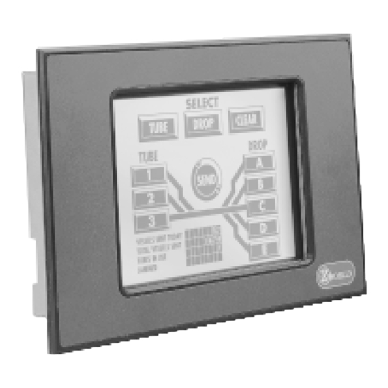
Initial OP7100 Setup Parts Required Setting Up the OP7100 DCIN (12–30 VDC) DCIN 485 + to power 485– supply 485+ 485– Figure 2-1. OP7100 Power Supply Connections wrong 18 s Getting Started OP7100... - Page 19 SUPPORT Figure 2-2. OP7100 Demo Screens OP7100 Getting Started s 19...
-
Page 20: Connecting The Op7100 To A Host Pc
Connecting the OP7100 to a Host PC CAUTION: High-Voltage Transformer. Only qualified persons may open this case. CONTRAST RS232 n.c. n.c. 232_RX1/ CT 232_TX1/ RT n.c. PWR_DE9 DCIN (12–30 VDC) 485 + 485– S/N: Figure 2-3. OP7100 Back Cover Option 1... - Page 21 Pin 1 PRGM PORT Marked Conductor to Pin 1 Figure 2-4. SIB Programming Connection To PC J4 SIB2 Figure 2-5. Direct Programming Connection OP7100 Getting Started s 21...
-
Page 22: Running Dynamic C
Running Dynamic C Serial Options OPTIONS OPTIONS Target Not Responding Communication Error <Ctrl Y> DEFDEMOL.C SAMPLES\QVGA 22 s Getting Started OP7100... - Page 23 ARDWARE HAPTER OP7100 Hardware s 23...
-
Page 24: Op7100 Subsystems Overview
Z180 SRAM Flash1 Flash2 ’691 Batt. super. RS-232 Control VRAM1 VRAM2 EPLD RS-485 Backlight 320 x 240 Drive Keypad Interface Sense Buzzer Contrast Adjustment Optional Software Touchscreen Contrast Adjustment Figure 3-1. OP7100 Block Diagram Computing Module 24 s Hardware OP7100... -
Page 25: Power Management
Sw Reg 2951 Lin Power J11:5 12–30 V DC 7662 7662 Sw Reg Sw Reg 300 V rms, 32.7 kHz, Backlight to CCFL backlight Power from EPLD Figure 3-2. Block Diagram of OP7100 Internal Power Regulators OP7100 Hardware s 25... -
Page 26: Adm691 Supervisor Chip
ADM691 Supervisor Chip Handling Power Fluctuations NMI. 1.3 V 26 s Hardware OP7100... - Page 27 NMI_BIT, a ; check for status of /PFO z,loop ; wait until the brownout ; clears timeout: ; then...a tight loop to ; force a watchdog timeout, timeout ; resetting the Z180 #endasm hitwd Watchdog Timer OP7100 Hardware s 27...
- Page 28 ) wd _ cleanup(); hitwd(); Power Shutdown and Reset /RESET PFI “Early Warning” /NMI /RESET 28 s Hardware OP7100...
-
Page 29: Memory Protection
U12 Supervisor DCIN VOUT VOUT VBAT 10 kW 47 µF 29.4 kW PFI to supervisor INT1 4.99 kW 220 kW Figure 3-3. OP7100 Power-Failure Detection Circuit − ... -
Page 30: Contrast Adjustment
SED1335F VRAMCS1 VRAMCS2 LCD Control FRAME ON/OFF XD[0–3] 10 kΩ 2.5 kΩ Manual ADJUST Software Contrast Adjustment Figure 3-4. Block Diagram LCD Control and Memory Contrast Adjustment CONTRAST Figure 3-5. Location of OP7100 Manual Contrast Adjustment 30 s Hardware OP7100... - Page 31 Software Manual Contrast Contrast Adjustment Adjustment OP7100 OP7110 Figure 3-6. Contrast Control Jumper Configurations Background 10 12 9 11 Positive Background (white with blue graphics) 10 12 9 11 Negative Background (blue with white graphics) Figure 3-7. LCD Background Jumper Settings...
-
Page 32: Coordinate Systems
Coordinate Systems Touchscreen 320,0 landscape landscape 0,240 320,240 240,0 portrait portrait 0,320 240,320 Figure 3-8. Coordinate Systems (row, column) 32 s Hardware OP7100... -
Page 33: Keypad Interface
COL2 ROW3 COL3 ROW4 COL4 ROW5 COL5 ROW6 COL6 ROW7 COL7 Figure 3-9. OP7100 Headers J5 and J6 (Keypad Interface) U8, U9 ROW[0–7] Q[0–7] Keypad/Buzzer drive To J5 (or to J6) keypad connectors 47 kΩ COL[0–7] D[0–7] Keypad sense Y[0–7] A[0–7]... - Page 34 To Z180 DIN[0–7] Data CMOS Input Figure 3-11. OP7100 Digital Inputs 10 12 14 16 18 20 22 24 26 28 30 32 34 9 11 13 15 17 19 21 23 25 27 29 31 33 Figure 3-12. OP7100 Header J7...
-
Page 35: Serial Communication
TX1/RTS RTS0 to J10 (DE9) T2IN T2OUT RXA0 RXA0 and J8 R1OUT R1IN RX1/CTS CTS0 R2OUT R2IN 232A Figure 3-13. Serial Channels 5-wire RS-232, 3-wire RS-232, RS-485 3-wire RS-232 RS-485 Figure 3-14. Serial Communication Jumper Configurations OP7100 Hardware s 35... - Page 36 RS-485 on RS-232 on header J11 header J11 Figure 3-15. Serial Communication Options for External Plug Connector (Header J11) 36 s Hardware OP7100...
- Page 37 RS-232 Communication Figure 3-16. RS-232 Signals Receive and Transmit Buffers OP7100 Hardware s 37...
-
Page 38: Modem Communication
CTS/RTS Control Modem Communication Modem OP7100 Side Side Figure 3-17. Connections Between Controller and Modem 38 s Hardware OP7100... - Page 39 485– Network Figure 3-18. RS-485 Signals CAUTION: High-Voltage Transformer. Only qualified persons may open this case. CONTRAST RS232 n.c. n.c. 232_RX1/ CT 232_TX1/ RT n.c. PWR_DE9 DCIN (12–30 VDC) 485+ 485– S/N: Figure 3-19. RS-485 Network OP7100 Hardware s 39...
- Page 40 Termination Resistors “Enabled” Termination Resistors “Disabled” Figure 3-20. Enabling/Disabling Termination Resistors 40 s Hardware OP7100...
-
Page 41: Use Of The Serial Ports
Status Register, Serial Channel 0 STAT1 Status Register, Serial Channel 1 TDR0 Transmit Data Register, Serial Channel 0 TDR1 Transmit Data Register, Serial Channel 1 RDR0 Receive Data Register, Serial Channel 0 RDR1 Receive Data Register, Serial Channel 1 OP7100 Hardware s 41... - Page 42 Z180 Serial Ports Z180 Z180 /RTS /DCD Microprocessor Internal Bus RDR0 TDR0 RXA0 RSR0 TSR0 TXA0 Shift Register In Shift Register Out /RTS0 CKA0 CNTLA0 Baud-Rate /CTS0 Generator CNTLB0 /DCD0 STAT0 Figure 3-21. Z180 Serial Channel 0 42 s Hardware OP7100...
- Page 43 /CTS /CTS /CTS interrupt-driven /DCD0 /DCD0 Table 3-3. Serial Port Interrupt Vectors Address Name Description Z180 Serial Port 0 (higher priority) SER0_VEC Z180 Serial Port 1 SER1_VEC OP7100 Hardware s 43...
-
Page 44: Asynchronous Serial Communication Interface
/DCD0 TDRE R / W R / W (05H) STAT1 RDRF OVRN CTS1E TDRE R / W R / W /DCD0 (Data Carrier Detect) /DCD0 /DCD0 TIE (Transmitter Interrupt Enable) TDRE (Transmitter Data Register Empty) /CTS 44 s Hardware OP7100... - Page 45 CTS1E (CTS Enable, Channel 1) RIE (Receiver Interrupt Enable) /DCD0 FE (Framing Error) PE (Parity Error) OVRN (Overrun Error) RDRF (Receiver Data Register Full) /DCD0 OP7100 Hardware s 45...
-
Page 46: Asci Control Register A
R / W MOD0–MOD2 (Data Format Mode Bits) Þ Þ Þ Þ Þ Þ MPBR/EFR (Multiprocessor Bit Receive/Error Flag Reset) /RTS0 (Request to Send, Channel 0) CKA1D (CKA1 Disable) Þ Þ TE (Transmitter Enable) Þ Þ 46 s Hardware OP7100... -
Page 47: Asci Control Register B
SS (Source/Speed Select) Table 3-4. Baud Rate Divide Ratios for Source/Speed Select Bits Divide Ratio ÷ 1 ÷ 2 ÷ 4 ÷ 8 ÷ 16 ÷ 32 ÷ 64 external clock* May not exceed system clock ÷ 40 OP7100 Hardware s 47... - Page 48 Divide Processor Ratio External ÷10 Clock Clock ÷30 Figure 3-22. Z180 Baud-Rate Generator DR (Divide Ratio) PEO (Parity Even/Odd) Þ Þ /CTS/PS (Clear to Send/Prescaler) Þ /CTS Þ /CTS MP (Multiprocessor Mode) MPBT (Multiprocessor Bit Transmit) 48 s Hardware OP7100...
- Page 49 03 or 09 7200 14,400 23 or 29 2400 4800 04 or 0A 3600 7200 24 or 2A 1200 2400 05 or 0B 1800 3600 25 or 2B 1200 06 or 0C 1800 26 or 2C OP7100 Hardware s 49...
- Page 50 50 s Hardware OP7100...
- Page 51 OFTWARE HAPTER OP7100 Software s 51...
-
Page 52: Supplied Software
Supplied Software OP71L.LIB OP71P.LIB EZIOOP71.LIB OP71L.LIB OP71P.LIB Table 4-1. OP7100 Software Libraries Library Application AASCZ0.LIB Serial communication applications Z180 Serial Port 0 AASCZ1.LIB Serial communication applications Z180 Serial Port 1 BIOS.LIB BIOS routines DRIVERS.LIB General drivers OP71L.LIB Select one of these DC 32 libraries to #use first, OP71P.LIB... - Page 53 0x4142,1 ); outport( 0x4147,0 ); inport & if( inport(0x4140) & 0x04 ) if( inport(0x4140) & 0x80 ) IBIT if( IBIT(0x4140,2) ) if( inport(0x4140) & 0x04 ) IBIT ISET IRES ISET IRES Dynamic C Function Reference OP7100 Software s 53...
- Page 54 ){ unsigned wAddr; for (;;) for(wAddr=0x4140;wAddr<0x4148;++wAddr){ outport( wAddr,0x01 ); printf( "%04x%02x\n",wAddr,inport(0x4140) ); delay( 0x8000 ); outport( wAddr,0x00 ); Real-Time Clock (RTC) DRIVERS.LIB Dynamic C Function Reference • tm _ rd • tm _ wr 54 s Software OP7100...
- Page 55 DRIVERS.LIB • int WriteFlash( unsigned long physical_addr, char *buf, int count ) count physical _ adr xdata phy _ adr(array) xdata physical _ adr *buf count WriteFlash physical _ addr physical _ addr WriteFlash WriteFlash SYS.LIB OP7100 Software s 55...
- Page 56 • void op71Init( void ); • void op71BackLight( int isOn ); isOn • void op71Power( int isOn ); isOn • void op71SetContrast( unsigned level ); level • void op71BlankScreen( void ); • void op71FillScreen( char pattern ); 56 s Software OP7100...
- Page 57 • void op71BuffUnlock( void ); • void op71SetBrushType( int type ); type GL _ SET OP71BLACK GL _ CLEAR OP71WHITE GL _ XOR OP71XOR oldPixel xor newPixel GL _ BLOCK OP71BLACK • int op71GetBrushType( void ); OP7100 Software s 57...
- Page 58 • void op71Right1( int left, int top, int cols, int rows ); left cols rows • void op71Up1( int left, int top, int cols, int rows ); left cols rows op71Left1 op71Right1 op71Up1 op71Down1 58 s Software OP7100...
- Page 59 • void op71HScroll( int left, int top, int cols, int rows, int nPix ); left cols rows nPix • void op71VScroll( int left, int top, int cols, int rows, int nPix ); left cols rows nPix OP7100 Software s 59...
- Page 60 • void op71XPutFastmap( int left, int top, int width, int height, unsigned long bitmap ); xmem op71XPutBitmap left width height bitmap xmem • void op71XGetBitmap( int x, int y, int bmWidth, int bmHeight, unsigned long xBm ); xmem op71XGetFastmap bmWidth bmHeight xmem 60 s Software OP7100...
- Page 61 • void op71PlotDot( int x, int y ); • void op71PlotLine( int x0, int y0, int x1, int y1 ); x0 y0 x1 y1 • void op71Block( int x, int y, int bmWidth, int bmHeight ); bmWidth bmHeight OP7100 Software s 61...
- Page 62 • void op71PlotVPolygon( int n, int *pFirstCoord ); pFirstCoord • void op71FillVPolygon( int n, int *pFirstCoord ); pFirstCoord • void op71PlotPolygon( int n, int x1, int y1, int x2, int y2, ... ); x1 y1 x2 y2 62 s Software OP7100...
- Page 63 • unsigned long op71FontChar( unsigned long font, char letter ); font xmem letter xmem • void op71PutFont( int x, int y, struct _fontInfo *pInfo, char code ); pInfo code OP7100 Software s 63...
- Page 64 • void op71SetPfStep( int stepX, int stepY ); op71Printf op71GetPfStep stepX op71Printf stepY op71Printf • void op71Printf( int x, int y, struct _ fontInfo *pInfo, char *fmt, ... ); printf op71SetPfStep op71GetPfStep pInfo Keypad Programming KP _ OP71.LIB 64 s Software OP7100...
- Page 65 • void eioBeep( int onOff ) onOff GLCD.LIB • void glFontInit( struct _fontInfo *pInfo, char pixWidth, char pixHeight, unsigned startChar, unsigned endChar, char *bitmapBuffer ) xmem glXFontInit pInfo pixWidth pixWidth pixHeight pixHeight startChar endChar bitmapBuffer OP7100 Software s 65...
- Page 66 Pixels specified by subsequent gl LCDPix = GL_XOR functions will toggle the LCD pixels LCDPix ^ newPix Pixels specified by subsequent gl functions will be displayed on the LCDPix = newPix GL_BLOCK LCD as is GL _ BLOCK glPlot glFill 66 s Software OP7100...
- Page 67 • void glPrintf( int x, int y, struct _fontInfo *pInfo, char *fmt,... ) printf *pInfo *fmt • void glPlotCircle( int xc, int yc, int rad ) • void glFillCircle( int xc, int yc, int rad ) OP7100 Software s 67...
- Page 68 • void glFillVPolygon( int n, int *pFirstCoord ) *pFirstCoord • void glFillPolygon( int n, int x1, int y1, int x2, int y2,... ) • void glPutBitmap( int x, int y, int bmWidth, int bmHeight, char *bm ) xmem glXPutBitmap bmWidth bmHeight 68 s Software OP7100...
- Page 69 • void glXPutBitmap( int x, int y, int bmWidth, int bmHeight, unsigned long bmPtr ) glPutBitmap bmWidth bmHeight bmPtr KP _ OP71.LIB • void kpInit( int (*changeFn)() ) kpDefInit changeFn kpScanState kpScanState • int kpScanState() kpInit OP7100 Software s 69...
- Page 70 • int kpDefStChgFn( char *curState, char *changed ) kpDefGetKey kpScanState kpDefGetKey curState changed kpScanState 8*row+col+edge*256 edge • int kpDefGetKey() kpDefStChgFn kpScanState kpDefInit kpDefGetKey 8*row+col+edge*256 edge • void kpDefInit() kpScanState kpDefGetKey 70 s Software OP7100...
- Page 71 SYS.LIB • int sysChk2ndFlash( struct _ flashInfo *pInfo ) struct _ flashInfo pInfo • void sysRoot2FXmem( struct _ flashInfo *pInfo, void *src, unsigned long int dest, unsigned integer len ) struct _ flashInfo pInfo sysChk2ndFlash dest OP7100 Software s 71...
- Page 72 72 s Software OP7100...
- Page 73 RAPHICS ROGRAMMING HAPTER OP7100 Graphics Programming s 73...
-
Page 74: Drawing Primitives
Initialization Drawing Primitives Plot a Pixel • int op71PlotDot(int x, int y); 74 s Graphics Programming OP7100... - Page 75 • void op71FillCircle(int xc, int yc, int rad); Fill a Polygon • void op71FillPolygon(int n, int x1, int y1,...); Draw a Bitmap • void op71XPutBitmap( int left, int top, int width, int height, unsigned long bitmap ); OP7100 Graphics Programming s 75...
-
Page 76: Font And Bitmap Conversion
Font and Bitmap Conversion List files of type File name Font files Bitmap files List files of type 76 s Graphics Programming OP7100... - Page 77 Using the Font/Bitmap In Your Program /*make call to op71XFontInit(&fi, 6, 8, 32, 127, fontBitMap)*/ OP7100 Graphics Programming s 77...
-
Page 78: Printing Text
Printing Text 78 s Graphics Programming OP7100... -
Page 79: Keypad Programming
Keypad Programming Initialization Scanning the Keypad Reading Keypad Activities OP7100 Graphics Programming s 79... - Page 80 80 s Graphics Programming OP7100...
- Page 81 NSTALLATION HAPTER OP7100 Installation s 81...
- Page 82 Grounding 82 s Installation OP7100...
-
Page 83: Installation Guidelines
FGND 0 V/GND External Ground Bezel/Casing to Power Supply GND FGND 0 V/GND External Ground Bezel/Casing to External Ground Figure 6-1. Location of Header JP5 Installation Guidelines OP7100 Installation s 83... - Page 84 Mounting Bezel-Mount Installation CUTOUT 0.125 D, 8x 0.180 1.620 (4.5) (40) 5.380 (137) 7.000 (178) Figure 6-2. Recommended Cutout Dimensions 84 s Installation OP7100...
-
Page 85: General Mounting Recommendations
OP7100 Bezel/Gasket Bracket Panel CAUTION: High-Voltage Transformer. Only qualified persons may open this case. CONTRAST RS232 n.c. n.c. 232_RX1/ CT 232_TX1/ RT n.c. PWR_DE9 DCIN (12–30 VDC) 485 + 485– S/ N: Figure 6-3. Strengthening Bracket General Mounting Recommendations OP7100... - Page 86 86 s Installation OP7100...
- Page 87 ROUBLESHOOTING PPENDIX OP7100 Troubleshooting s 87...
- Page 88 Out of the Box 88 s Troubleshooting OP7100...
-
Page 89: Dynamic C Will Not Start
Dynamic C Will Not Start Wrong Communication Mode Wrong COM Port Wrong Operating Mode Dynamic C Loses Serial Link OP7100 Repeatedly Resets hitwd OP7100 Troubleshooting s 89... -
Page 90: Common Programming Errors
Type Range –32,768 (–2 ) to +32,767 (2 – 1) −2,147,483,648 (−2 long int ) to +2147483647 (2 – 1) float 1.18 × 10 3.40 × 10 char 0 to 255 3293 3293.0 float && & 90 s Troubleshooting OP7100... - Page 91 PECIFICATIONS PPENDIX OP7100 Specifications s 91...
-
Page 92: Electrical And Mechanical Specifications
4.803 (25) (122) 6.299 (160) 6.579 (167) Figure B-1. OP7100 LCD Dimensions Bezel Dimensions 0.125R typ. (3.18) 4-40-4 screws, 4x LCD aperture is 122 x 92 mm Pixel matrix (320 x 240) is 115.17 x 86.37 mm 4-40-8 screws, 8x 0.125R, typ... -
Page 93: General Specifications
General Specifications Table B-1. OP7100 General Specifications Parameter Specification 6.63" × 4.40" × 1.36" Module Size (168 mm × 112 mm × 35 mm) 8.00" × 5.4" × 0.156" (203 mm × 137 mm × 4.0 mm) Bezel Size with gasket Package Size 8.0"... -
Page 94: Header And Jumper Configurations
KEYPAD DANGER! HIGH VOLTAGE RS485 TERM. RS232 PRGM DIGITAL I/O PORT Figure B-3. OP7100 Headers Table B-2. OP7100 Signal Headers Header Description LCD (hard-wired) Backlight LCD (ribbon cable) Programming port Touchscreen interface (OP7100 only) Keypad interface (OP7110 only) Digital I/O... - Page 95 Table B-3. OP7100 Jumper Settings Pins Factory Header Function Connected Default 1–2 Positive LCD background 5–6 (blue characters on white 7–8 background) 11–12 1–3 Negative LCD background 4–6 (white characters on blue 7–9 background) 10–12 1–2 Software contrast adjustment OP7100 2–3...
- Page 96 96 s Specifications OP7100...
- Page 97 EMORY PPENDIX I/O M NTERRUPT ECTORS OP7100 Memory, I/O Map, and Interrupt Vectors s 97...
-
Page 98: Op7100 Memory
OP7100 Memory 1024K Socket U8 512K 0x80000 Socket U7 EPROM 0x00000 Figure C-1. Memory Map of 1M Address Space XMEM XMEM UNITIALIZED UNITIALIZED DATA DATA STACK STACK UNUSED UNUSED USER CODE USER CODE LIBRARY LIBRARY RAM-Based ROM-Based Figure C-2. Memory Map of 64K Virtual Space... -
Page 99: Execution Timing
Floating add (p+q;) (typical) Floating multiply (p*q;) Floating divide (p/q;) Long add (l+m;) Long multiply (l*m;) Long divide (l/m;) Floating square root (sqrt(q);) Floating exponent (exp(q);) 2503 Floating cosine (cos(q);) 3049 OP7100 Memory, I/O Map, and Interrupt Vectors s 99... -
Page 100: Memory Map
Timer Data Register Channel 1, least 0x15 TMDR1H Timer Data Register Channel 1, most 0x16 RLDR1L Timer Reload Register Channel 1, least 0x17 RLDR1H Timer Reload Register Channel 1, most continued… 100 s Memory, I/O Map, and Interrupt Vectors OP7100... - Page 101 Reserved 0x38 MMU Common Base Register 0x39 MMU Bank Base Register 0x3A CBAR MMU Common/ Bank Area Register 0x3B–0x3D — Reserved 0x3E OMCR Operation Mode Control Register 0x3F I/O Control Register OP7100 Memory, I/O Map, and Interrupt Vectors s 101...
- Page 102 10 months 0x418A YEAR1 D7–D0 years 0x418B YEAR10 D7–D0 10 years 0x418C WEEK D7–D0 day of week 0x418D TREGD D7–D0 Register D 0x418E TREGE D7–D0 Register E 0x418F TREGF D7–D0 Register F 102 s Memory, I/O Map, and Interrupt Vectors OP7100...
-
Page 103: Other Registers
Chip Select 4 4100–413F Chip Select 5 COLUMN 4140–417F Chip Select 6 41C0–41FF Watchdog WDOG 8000 Flash EPROM write enable FSHWE A000 Bit 0 is the power-failure (NMI) state. C000 Watchdog output OP7100 Memory, I/O Map, and Interrupt Vectors s 103... -
Page 104: Interrupt Vectors
Available for programming (CM7200), not CSI/O_VEC available for use on CM7100 0x0E Asynchronous Serial Port Channel 0 SER0_VEC 0x10 Asynchronous Serial Port Channel 1 SER1_VEC #INT _ VEC 0x10 myfunction myfunction() interrupt interrupt myfunction() { 104 s Memory, I/O Map, and Interrupt Vectors OP7100... - Page 105 // input voltage is still below the threshold // that triggered the NMI return; // if just a power glitch, return Jump Vectors #JUMP_VEC NMI_VEC name OP7100 Memory, I/O Map, and Interrupt Vectors s 105...
-
Page 106: Interrupt Priorities
INT 2 (maskable interrupts, Level 2) PRT Timer Channel 0 PRT Timer Channel 1 DMA Channel 0 DMA Channel 1 Z180 Serial Port 0 (Lowest Priority) Z180 Serial Port 1 106 s Memory, I/O Map, and Interrupt Vectors OP7100... - Page 107 PPENDIX ERIAL NTERFACE OARD OP7100 Serial Interface Board 2 s 107...
- Page 108 Introduction Reset Target 108 s Serial Interface Board 2 OP7100...
-
Page 109: External Dimensions
External Dimensions 2.25 (57.2) Top View 12.0 3.60 (305) (91.4) (20) 1.525 1.625 (38.7) (41.3) Side View Figure D-1. SIB External Dimensions OP7100 Serial Interface Board 2 s 109... - Page 110 110 s Serial Interface Board 2 OP7100...
- Page 111 ACKUP ATTERY PPENDIX OP7100 Backup Battery s 111...
-
Page 112: Battery Life And Storage Conditions
Battery Life and Storage Conditions Replacing the Lithium Battery 112 s Backup Battery OP7100... -
Page 113: Battery Cautions
Battery Cautions (English) (German) (French) (Spanish) (Dutch) (Swedish) OP7100 Backup Battery s 113... - Page 114 114 s Backup Battery OP7100...
- Page 115 NDEX Symbols #INT_VEC #JUMP_VEC #use /CS1 /CS6 /CTS /CTS/PS /DCD0 /NMI /RESET /RTS0 /RTS1 /TEND0 /WDO CKA1 CKA1 CKA1/~TEND0 CKA1D OP7100 Index s 115...
- Page 116 CSI/O float fntcvtr.exe CTS1 fntstrip.exe 116 s Index OP7100...
- Page 117 IEF1 IEF2 OP7100 Index s 117...
- Page 118 OVRN MOD0 MOD1 MOD2 MPBR/EFR MPBT NMI _ VEC NO _ CARRIER 118 s Index OP7100...
- Page 119 RDRF RETN IBIT inport IRES ISET outport EZIOOP71.LIB eioBeep RTS0 op71BackLight op71SetContrast OP7100 Index s 119...
- Page 120 AASCZ0.LIB op71Power AASCZ1.LIB op71Printf BIOS.LIB op71PutFont DRIVERS.LIB op71Right1 EZIOOP71.LIB op71SetBrushType GLCD.LIB op71SetBrushType KP _ OP71.LIB LQVGA.LIB op71SetContrast OP71HW.LIB op71SetPfStep OP71L.LIB op71VScroll OP71P.LIB op71XFontInit PQVGA.LIB op71XGetBitmap SYS.LIB op71XGetFastmap op71XPutBitmap op71XPutFastmap 120 s Index OP7100...
- Page 121 WriteFlash SYS.LIB sysChk2ndFlash sysRoot2FXmem tm _ rd tm _ wr TRAP source STAT0 TDRE wderror OP7100 Index s 121...
- Page 122 122 s Index OP7100...
Need help?
Do you have a question about the OP7100 and is the answer not in the manual?
Questions and answers