
Related Manuals for Micom P631


Summary of Contents for Micom P631
- Page 1 MiCOM P631 Transformer Differential Protection Device P631/EN M/R-11-C Version P631 -310 -409/410 -650 Technical Manual...
- Page 3 General Note on the PDF Version of this Technical Manual All entries in the Table of Contents and all cross-references to other sections, figures etc. in green letters are hyperlinks, i.e. by a single mouse click on the reference one can navigate directly to the referenced part of the manual. In the Adobe Reader (or the Acrobat Pro), one can return back to the previous view by using the menu point View / Page Navigation / Previous View (keyboard shortcut: ALT + Left cursor key).
- Page 5 Electric strongly recommends that these output relays are hardwired into the substation's automation system, for alarm purposes. Any modifications to this P631 must be in accordance with the manual. If any other modification is made without the express permission of Schneider Electric, it will invalidate the warranty, and may render the product unsafe.
- Page 6 Note This operating manual gives instructions for installation, commissioning and operation of the P631. However, the manual cannot cover all conceivable circumstances or include detailed information on all topics. In the event of questions or specific problems, do not take any action without proper authorization.
- Page 7 Changes after going to press...
-
Page 9: Table Of Contents
P631 TABLE OF CONTENTS APPLICATION AND SCOPE ................... 1-1 Overview - P631 ......................1-1 Including Function Groups in the Configuration ............1-3 Overview of Function Groups - Part 1 ................. 1-4 Overview of Function Groups - Part 2 ................. 1-6 Design .........................1-8 Configurable Function Keys .................. - Page 10 3.11.2 Layout of the LED Indicators ........................3-59 3.11.3 Operating Mode of the LED Indicators ......................3-60 3.12 Main Functions of the P631 (Function Group MAIN) ..........3-62 3.12.1 Conditioning of the Measured Values ......................3-62 3.12.2 Phase Reversal Function ..........................3-65 3.12.3...
- Page 11 Inverse-time Overcurrent Protection (Function Groups IDMT1 and IDMT2) .... 3-131 3.23.1 Enabling or Disabling IDMT Protection .......................3-131 3.23.2 Time-Dependent Characteristics ....................... 3-133 3.23.3 Phase Current Stage ..........................3-136 3.23.4 Negative-Sequence Current Stage ......................3-138 3.23.5 Residual Current Stage ..........................3-140 3.23.6 Hold Time ..............................3-142 P631/EN M/R-11-C // P631-310-650...
- Page 12 Dimensional Drawings for the 40 TE Case .....................4-4 4.2.2 Detachable HMI ............................. 4-5 Hardware Modules ...................... 4-7 INSTALLATION AND CONNECTION ...............5-1 Unpacking and Packing ....................5-2 Checking Nominal Data and Design Type ..............5-3 Location Requirements ....................5-4 P631/EN M/R-11-C // P631-310-650...
- Page 13 Connecting the Serial Interfaces ......................... 5-14 Location and Connection Diagrams ................5-18 5.7.1 Location Diagrams P631‑409/410 ........................5-18 5.7.2 Terminal Connection Diagrams P631‑409/410 .................... 5-18 LOCAL CONTROL (HMI) ..................6-1 Local Control Panel (HMI) ....................6-1 Display and Keypad ....................6-2 6.2.1 Text Display ..............................6-2...
- Page 14 12.2 Routine Functional Testing ..................12-3 12.3 Analog Input Circuits ....................12-4 12.4 Binary Opto Inputs ....................12-5 12.5 Binary Outputs ......................12-6 12.6 Serial Interfaces ......................12-7 STORAGE ......................13-1 ACCESSORIES AND SPARE PARTS ..............14-1 P631/EN M/R-11-C // P631-310-650...
- Page 15 A4 TELECONTROL INTERFACES ................A4-1 A4.1 Telecontrol Interface per EN 60870-5-101 or IEC 870-5-101 (Companion Standard) ..........................A4-1 A4.1.1 Interoperability ............................A4-1 A4.2 Communication Interface per IEC 60870-5-103 ............A4-9 A4.2.1 Interoperability ............................A4-9 A5 P631 VERSION HISTORY ................... A5-1 P631/EN M/R-11-C // P631-310-650...
- Page 16 P631 Table of Contents P631/EN M/R-11-C // P631-310-650...
-
Page 17: Application And Scope
These features give the user the means to adapt the P631 to the protection and control capacity required in a specific application. The powerful programmable logic provided by the protection device also makes it possible to accommodate special applications. - Page 18 DIFF DTOC1 IDMT1 THRM1 CBF_1 MCM_1 MCM_2 LOGIC / LOG2 Optional Always available SIG_1 CMD_1 MEASI MEASO Transformer Differential Protection P631 Fig. 1-2: Function diagram For a list of all available function groups see the Appendix. P631/EN M/R-11-C // P631-310-650...
-
Page 19: Including Function Groups In The Configuration
MiCOM S1 operating program. Unused or cancelled function groups are hidden to the user, thus simplifying the menu of the MiCOM S1. -
Page 20: Overview Of Function Groups - Part 1
1 Application and Scope Overview of Function Groups - Part 1 The following tables list the function groups that can be included in or excluded from the configuration of the P631. ✓ = Standard; (✓) = Ordering option. Protection functions... - Page 21 IEC 61850 Function group P631 Abbrev. Description RtdGGIO1 MEASI Analog inputs and outputs (✓) IdcGGIO1 MEASO RTD input (✓) ● 1× Measuring data input 20 mA (✓) ● 2× Measuring data output 20 mA (✓) ● P631/EN M/R-11-C // P631-310-650...
-
Page 22: Overview Of Function Groups - Part 2
1 Application and Scope Overview of Function Groups - Part 2 The following tables list the function groups that are generally available for the P631, and which cannot be excluded from the configuration. ✓ = Standard; (✓) = Ordering option. Inputs and outputs... - Page 23 PTRCx / FT_RC Fault recording (time-tagged event logging together ✓ RDRE1 with fault value recording of the three phase currents, the residual current as well as the three phase-to-ground voltages and the neutral-point displacement voltage) P631/EN M/R-11-C // P631-310-650...
-
Page 24: Design
P631 1 Application and Scope Design The P631 is modular in design. The plug-in modules are housed in a robust aluminum case and electrically interconnected via one analog p/c board and one digital p/c board. P631/EN M/R-11-C // P631-310-650... -
Page 25: Configurable Function Keys
P631 1 Application and Scope Configurable Function Keys To the right of the text display, there are six freely configurable function keys available. These may be used for easy control operation access. P631/EN M/R-11-C // P631-310-650... -
Page 26: Inputs And Outputs
1 Application and Scope Inputs and Outputs The nominal current and voltage values of the measuring inputs on the P631 can be set with the function parameters. The nominal voltage range of the optical coupler inputs is 24 to 250 V DC. As an option binary signal input modules with a higher operate threshold are available. -
Page 27: Control And Display
● assignment for the colors red and green. Furthermore there are various operating modes and flashing functions available. PC interface. ● One or two communication interface(s) for connection to a substation ● control system (optional). P631/EN M/R-11-C // P631-310-650 1-11... -
Page 28: Information Interfaces
Information is exchanged through the local control panel, the PC interface, or two optional communication interfaces (channel 1 and channel 2). Using the first channel of the communication interfaces (COMM1), the P631 can be wired either to the substation control system or to a telecontrol system. This channel is optionally available with a switchable protocol (per IEC 60870‑5‑103,... -
Page 29: Technical Data
Applicable to P631, version -310 -409/410 -650. Declaration of Conformity The product designated “P631 Transformer Differential Protection Device” has been designed and manufactured in conformance with the European standards EN 60255‑26 and EN 60255‑27 and with the “EMC Directive” and the “Low Voltage Directive”... -
Page 30: General Data
® is a registered trademark of AT&T Lightguide Cable Connectors.) Wire leads (X9, X10) ● M2 threaded terminal ends for wire cross-sections up to 1.5 mm² (US: ■ AWG16). IRIG-B Interface (X11) ● BNC plug ■ P631/EN M/R-11-C // P631-310-650... - Page 31 0.2 to 2.5 mm² (US: AWG25 to AWG14), or Threaded terminal ends, ring-type cable lugs: M4. ● Creepage Distances and Clearances Per EN 60255-27. ● Pollution degree 3, working voltage 250 V, ● overvoltage category III, impulse test voltage 5 kV. ● P631/EN M/R-11-C // P631-310-650...
-
Page 32: Tests
Amplitude: 2 kV / 1 kV or 4 kV / 2 kV. ● Burst duration:15 ms. ● Burst period: 300 ms. ● Burst frequency: 5 kHz. ● Source impedance: 50 Ω. ● Power Frequency Immunity Per IEC 60255‑22‑7, Class A: P631/EN M/R-11-C // P631-310-650... - Page 33 The PC interface must not be subjected to the voltage test. Impulse Voltage Withstand Test Per EN 60255-27. Front time: 1.2 µs ● Time to half-value: 50 µs ● Peak value: 5 kV ● Source impedance: 500 Ω ● P631/EN M/R-11-C // P631-310-650...
- Page 34 Shock Response tests are carried out to verify full operability (during ● operation), test severity class 1: 5 g for 11 ms. Shock Withstand tests are carried out to verify the endurance (during ● transport), test severity class 1: 15 g for 11 ms. P631/EN M/R-11-C // P631-310-650...
-
Page 35: Routine Tests
Per EN 60255-27. 2.2 kV AC, 1 s ● Only direct voltage (2.8 kV DC) must be used for the voltage test on the power supply inputs. The PC interface must not be subjected to the voltage test. P631/EN M/R-11-C // P631-310-650... - Page 36 P631 2 Technical Data Additional Thermal Test 100% controlled thermal endurance test, inputs loaded. ● P631/EN M/R-11-C // P631-310-650...
-
Page 37: Environmental Conditions
≤ 75 % relative humidity (annual mean). ● 56 days at ≤ 95 % relative humidity and 40°C [104°F]. ● Condensation not permitted. ● Solar Radiation Direct solar radiation on the front of the device must be avoided. P631/EN M/R-11-C // P631-310-650... -
Page 38: Inputs And Outputs
Nominal consumption per phase: < 0.1 VA at I ● Load rating: ● continuous: 20 A, ■ for 10 s: 150 A, ■ for 1 s: 500 A. ■ Nominal surge current: 1250 A. ● 2-10 P631/EN M/R-11-C // P631-310-650... -
Page 39: Binary Signal Inputs
19 V. Special versions with higher pick-up/drop-off thresholds are provided for applications where a higher switching threshold is expressly required. The maximum voltage permitted for all binary signal inputs is 300 V DC. P631/EN M/R-11-C // P631-310-650 2-11... -
Page 40: Irig-B Interface
Open-circuit monitoring: Θ > +215°C and Θ < -40°C (Θ > +419°F and ● Θ < -40°F). 2.5.6 Direct Current Output Output current: 0 to 20 mA ● Maximum permissible load: 500 Ω ● Maximum output voltage: 15 V ● 2-12 P631/EN M/R-11-C // P631-310-650... -
Page 41: Output Relays
300 V DC. Operating time: less than 0.2 ms less than 5 ms Reset time: less than 8 ms less than 5 ms 2.5.8 BCD Measured Data Output Maximum numerical value that can be displayed: 399 P631/EN M/R-11-C // P631-310-650 2-13... -
Page 42: Interfaces
Optical input: max. -10 dBm ● Distance to be bridged: max. 400 m ● (Distance to be bridged given for identical optical outputs and inputs at both ends, a system reserve of 3 dB, and typical fiber attenuation) 2-14 P631/EN M/R-11-C // P631-310-650... -
Page 43: Iec Communication Interface
Optical output: min. −20 dBm ■ Optical sensitivity: min. −31 dBm ■ Optical input: max. −14 dBm ■ 2.6.5 IRIG‑B Interface B122 format ● Amplitude modulated signal ● Carrier frequency: 1 kHz ● BCD- coded variable data (daily) ● P631/EN M/R-11-C // P631-310-650 2-15... -
Page 44: Information Output
P631 2 Technical Data Information Output Counters, measured data, and indications: see chapter “Information and Control Functions”. 2-16 P631/EN M/R-11-C // P631-310-650... -
Page 45: Settings - Typical Characteristic Data
Operate time including output relay (measured variable from 0 to 2-fold ● operate value): ≤ 40 ms, approx. 30 ms Reset time (measured variable from 2-fold operate value to 0): ≤ 40 ms, ● approx. 30 ms Starting resetting ratio: approx. 0.95 ● P631/EN M/R-11-C // P631-310-650 2-17... -
Page 46: Deviations
Deviation: ± 5% ● 2.9.1.5 Thermal Overload Protection Operate value Θ Deviation: ± 5% ● 2.9.1.6 Frequency Protection Operate values f<> ± 30 mHz (f = 50 Hz) ● ± 40 mHz (f = 60 Hz) ● 2-18 P631/EN M/R-11-C // P631-310-650... -
Page 47: Deviations Of The Timer Stages
Inverse-time stages Deviation when I ≥ 2 I : ± 5% + 10 to 25 ms ● For “extremely inverse” IEC characteristics and for thermal overload ● characteristics: ± 7.5% + 10 to 20 ms P631/EN M/R-11-C // P631-310-650 2-19... -
Page 48: Deviations Of Measured Data Acquisition
Internal Clock With free running internal clock Deviation: < 1 min/month ● With external synchronization (with a synchronization interval ≤ 1 min) Deviation: < 10 ms ● With synchronization via IRIG-B interface ± 1 ms ● 2-20 P631/EN M/R-11-C // P631-310-650... -
Page 49: Resolution Of The Fault Data Acquisition
Currents Dynamic range 33·I ● Amplitude resolution at I = 1 A: 2.0 mA ● at I = 5 A: 10.1 mA ● 2.10.3 Voltage Dynamic range: 150 V ● Amplitude resolution: 9.2 mV ● P631/EN M/R-11-C // P631-310-650 2-21... -
Page 50: Recording Functions
Number The 8 most recent faults. ● Scope for signals and fault values All fault-relevant signals from a total of 1024 different logic state signals. ● Sampled values for all measured currents and voltages ● 2-22 P631/EN M/R-11-C // P631-310-650... - Page 51 820 periods in total for all faults, that is 16.4 s (for fnom = 50 Hz) or 13.7 s (for fnom = 60 Hz). Resolution of the Recorded Data As per Section 2.10, (p. 2-21), with maximum current dynamic ranges ● (100 I / 16 I N,nom P631/EN M/R-11-C // P631-310-650 2-23...
-
Page 52: Power Supply
< 3 A for duration of 0.25 ms ● Stored energy time ≥ 50 ms for interruption of V ≥ 220 V DC (upper range supply) ● ≥ 50 ms for interruption of V ≥ 60 V DC (lower range supply) ● 2-24 P631/EN M/R-11-C // P631-310-650... -
Page 53: Current Transformer Specifications
Secondary accuracy limiting voltage (e.m.f.) of the CT Rated knee point voltage (e.m.f.) of the CT Rated accuracy limit factor of the CT Actual accuracy limit factor of the CT: · · R ct + R b P ct + P b P631/EN M/R-11-C // P631-310-650 2-25... -
Page 54: General Equations
● A = wire cross section ● The MiCOM Px3x input CT burden R is less than 20 mΩ, independent of the set nominal current (1A or 5A). Usually this relay burden can be neglected. The rated knee point voltage V according to IEC 60044‑1-am1, 2.3.12 is lower... -
Page 55: Transformer Differential Protection
4 times the steady-state accuracy limit current of the CT. This corresponds to a dimensioning factor of K = 0.25 for internal faults. It is recommended to use CTs of accuracy class 5P (or equivalent). P631/EN M/R-11-C // P631-310-650 2-27... - Page 56 P631 2 Technical Data 2-28 P631/EN M/R-11-C // P631-310-650...
-
Page 57: Operation
OPERATION Modular Structure The P631, a numerical device, is part of the MiCOM P30 family of devices. The device types included in this family are built from identical uniform hardware modules. The figure below shows the basic hardware structure of the P631. - Page 58 The local control module L is located behind the front panel and connected to the processor module via a ribbon cable. It encompasses all control and display elements as well as a PC interface for running the operating program S1. P631/EN M/R-11-C // P631-310-650...
-
Page 59: Operator-Machine Communication
Display of Settings and Signals Settings and signals are displayed either in plain text or as addresses, in accordance with the user’s choice. All settings and signals of the P631 are documented in a separate collection of documents, the so-called “DataModelExplorer”. -
Page 60: Configuration Of The Measured Value Panels (Function Group Loc)
3 Operation Configuration of the Measured Value Panels (Function Group LOC) The P631 offers Measured Value Panels, which display the measured values relevant at a given time. During normal power system operation, the Operation Panel is displayed. If the Operation Panel is activated as an event occurs, the display switches to the appropriate Event Panel –... -
Page 61: Operation Panel
MAIN: General reset EXT [ 005 255 ] FT_RC: Reset record. USER [ 003 006 ] 1: execute FT_RC: Reset record. EXT [ 005 243 ] MAIN: Reset LED 306 020 63Z80CXA Fig. 3-2: Operation Panel. P631/EN M/R-11-C // P631-310-650... -
Page 62: Fault Panel
MAIN: General reset EXT [ 005 255 ] FT_RC: Reset record. USER [ 003 006 ] 1: execute FT_RC: Reset record. EXT [ 005 243 ] MAIN: Reset LED 306 020 50Z01EJA Fig. 3-3: Fault panel. P631/EN M/R-11-C // P631-310-650... -
Page 63: Overload Panel
Fig. 3-4: Overload Panel. 3.3.4 Configurable Clear Key The P631 has a Clear key – –, to which one or more reset functions can be assigned by selecting the required functions at LOC : F ct. r e set key. Details on the functions' resetting features are given in Section 3.12.11, (p. -
Page 64: Serial Interfaces
COMM2 becomes “dead”. It will only be enabled again when the “time-out” period for the PC interface has elapsed. If tests are run on the P631, the user is advised to activate the test mode. In this way the PC or the control system will recognize all incoming test signals accordingly (see Section 3.12.13, (p. -
Page 65: Pc Interface (Function Group Pc)
3 Operation 3.4.1 PC Interface (Function Group PC) Communication between the P631 and a PC is through the PC interface. In order for data transfer between the P631 and the PC to function, several settings must be made in the P631. -
Page 66: Communication Interface 1 (Function Group Comm1)
In order for data transfer to function properly, several settings must be made in the P631. Communication interface 1 can be blocked through a binary signal input. In addition, a signal or measured-data block can also be imposed through a binary signal input. 3-10 P631/EN M/R-11-C // P631-310-650... - Page 67 0: No 1: Yes COMM1: DNP3 enable [ 003 231 ] 0: No 1: Yes COMM1: COURIER enable [ 103 040 ] 0: No 1: Yes 64Z51FEA Fig. 3-6: Communication interface 1, selecting the interface protocol. P631/EN M/R-11-C // P631-310-650 3-11...
- Page 68 1: Yes [ 037 075 ] COMM1: Sig./meas. block EXT [ 037 074 ] MAIN: Prot. ext. disabled [ 038 046 ] 61Z70FFA Fig. 3-7: Communication interface 1, settings for the IEC 60870‑5-103 interface protocol. 3-12 P631/EN M/R-11-C // P631-310-650...
- Page 69 1: Yes [ 037 075 ] COMM1: Sig./meas. block EXT [ 037 074 ] MAIN: Prot. ext. disabled [ 038 046 ] 61Z51FGA Fig. 3-8: Communication interface 1, settings for the IEC 870-5-101 interface protocol. P631/EN M/R-11-C // P631-310-650 3-13...
- Page 70 Sig./meas.val.block. 1: Yes [ 037 075 ] COMM1: Sig./meas. block EXT [ 037 074 ] MAIN: Prot. ext. disabled [ 038 046 ] 61Z51FHA Fig. 3-9: Communication interface 1, settings for the ILS-C interface protocol. 3-14 P631/EN M/R-11-C // P631-310-650...
- Page 71 [ 003 170 ] 1: Yes COMM1: Commun. interface Communication error 304 422 COMM1: Command blocking [ 003 174 ] MAIN: Test mode [ 037 071 ] 19Z50FJB Fig. 3-10: Communication interface 1, settings for the MODBUS protocol. P631/EN M/R-11-C // P631-310-650 3-15...
- Page 72 General enable USER [ 003 170 ] 1: Yes COMM1: Command blocking [ 003 174 ] MAIN: Test mode Commun. interface [ 037 071 ] 64Z50AZA Fig. 3-11: Communication interface 1, settings for the DNP 3.0 protocol. 3-16 P631/EN M/R-11-C // P631-310-650...
- Page 73 0: No 1: Yes COMM1: Command blocking [ 003 174 ] MAIN: COMM1: Test mode Commun. interface Communication error [ 037 071 ] 304 422 19Z51BAA Fig. 3-12: Communication interface 1, settings for the COURIER protocol. P631/EN M/R-11-C // P631-310-650 3-17...
- Page 74 [ --- --- ] 0: don't execute 1: execute COMM1: Test spont.sig. end [ 003 186 ] COMM1: Spontan. sig. end [ --- --- ] 0: don't execute 1: execute 48Z50FKA Fig. 3-13: COMM1 – Checking spontaneous signals. 3-18 P631/EN M/R-11-C // P631-310-650...
-
Page 75: Communication Interface 2 (Function Group Comm2)
[ 103 053 ] [ 038 046 ] COMM2: Command block. USER [ 103 172 ] 0: No 1: Yes Commun. interface MAIN: Test mode [ 037 071 ] 64Z5189A Fig. 3-14: Settings for communication interface 2. P631/EN M/R-11-C // P631-310-650 3-19... - Page 76 [ --- --- ] 0: don't execute 1: execute COMM2: Test spont.sig. end [ 103 186 ] COMM2: Spontan. sig. end [ --- --- ] 0: don't execute 1: execute 48Z50FLA Fig. 3-15: COMM2 – Checking spontaneous signals. 3-20 P631/EN M/R-11-C // P631-310-650...
-
Page 77: Communication Interface Iec 61850 (Function Groups Iec, Goose And Gsse)
Function group IEC is only available as an alternative to function group COMM1 (hardware ordering option!). 3.4.4.1 Communication Interface IEC 61850 (Function Group IEC) The P631 offers as an ordering option a communication protocol according to the Ethernet based IEC 61850 protocol. 3.4.4.1.1 IEC 61850 IEC 61850 was created jointly by users and manufacturers as an international standard. - Page 78 The optional Ethernet module additionally provides an RS485 interface for remote access with the MiCOM S1 support software (function group COMM2). The P631 may be equipped with the optional Ethernet module only as an alternative to the standard optional communication module. Therefore the Ethernet-based communication protocol IEC 61850 is available only as an alternative to function group COMM1.
- Page 79 P631 3 Operation System configurator PACiS SCE .iid .scd .icd IED Configurator IED Configurator Operating program .mcl .x3v 19Z7001C Fig. 3-16: Configuration according to IEC 61850-6. P631/EN M/R-11-C // P631-310-650 3-23...
- Page 80 SNTP Server or Request from Server. With the first operating mode synchronization occurs by a broadcast message sent from the SNTP server to all devices in the network, and in the second operating mode the P631 requests a device-specific time signal during a settable cycle.
- Page 81 GOOSEs. The P631 can serve up to sixteen clients. Each client can log-on to any number of available reports. One unbuffered report can be allocated to max. 8 clients, and one buffered report can be allocated to max.
- Page 82 Including fault transmission for the IEC 61850 in the configuration is only possible with the IED Configurator. Transmission of fault files is supported per “File Transfer”. COMTRADE fault files in the P631 are transmitted uniformly either as ASCII or binary formatted files. Fault transmission can be cancelled from the configuration. 3.4.4.1.10...
- Page 83 Generic Object Oriented Substation Event (Function Group GOOSE) For high priority exchange of information between individual devices (IEDs) in a local network, the P631 provides the function group GOOSE as defined in the standard IEC 61850. GOOSE features high-speed and secure transmission of information for reverse interlocking, decentralized substation interlock, trip commands, blocking, enabling, contact position signals and other signals.
- Page 84 32 signals can be selected from all the signals available in the P631 to be transmitted via GOOSE, as it is also possible with reporting. Selection of binary state signals (shuttling to communications) is made by setting GO OSE: Output 1 fct.
- Page 85 (opto‑coupler inputs). Contact position signals received from external devices (LN: DevGosGGIO3) are listed in the selection table for interlocking equations of the function group ILOCK, which are available to design a decentralized substation interlock. P631/EN M/R-11-C // P631-310-650 3-29...
- Page 86 The state information is reset and accordingly signaled after termination of the command sequence. The P631 is capable to monitor the command status of up to 32 further devices. With the IED Configurator OrdRunGGIO1.ind1.stVal to OrdRunGGIO1.ind32.stVal are configured in a similar way to the other GOOSE inputs. A shuttling to the interlocking equations is not necessary as their consideration within command checking is automatically enabled when the first binary signal input is configured.
- Page 87 The function can then be enabled or disabled by setting G SSE : Gen er al e na ble U SER. The setting parameters for function groups IEC, GOOSE and GSSE in the P631 are not automatically activated. The P631 features two memory “banks” one of which includes the active setting parameters.
- Page 88 (e.g. GS SE: Inp ut 1 d efault). The various settings, measured values and signals for function group GOOSE are described in chapters 7 and 8. 3-32 P631/EN M/R-11-C // P631-310-650...
-
Page 89: Irig-B Clock Synchronization (Function Group Irigb)
If, for example, a GPS receiver with IRIG-B connection is available, the internal clock of the P631 can be synchronized to run on GPS time using the optional IRIG-B interface. It should be noted that the IRIG-B signal holds information on the day only (day of the current year). -
Page 90: Configurable Function Keys (Function Group F_Key)
3 Operation Configurable Function Keys (Function Group F_KEY) The P631 provides six freely configurable function keys. A password may be configured for each function key (e.g. for F1 at F _KEY: Passwor d funct .k ey 1), and if a password has been configured then the respective function key will only be enabled when the configured password is entered. - Page 91 [ 080 122 ] 1: Key 2: Switch & & & Keys, local control 40Z5003A Fig. 3-21: Configuration and operating mode of function keys. The assigned function is either a single function or a menu jump list. P631/EN M/R-11-C // P631-310-650 3-35...
-
Page 92: Configuration And Operating Mode Of The Binary Inputs (Function Group Inp)
In order to ensure that during normal operation the P631 will recognize an input signal, it must persist for at least 20 ms. With the occurrence of a general starting this time period may have to be increased to 40 ms under unfavorable conditions. - Page 93 -Uxxx & Input signal & & INP: Filter [ 010 220 ] & INP: State U xxx & [ ZZZ ZZZ ] & 12Z6213A Fig. 3-22: Configuration and operating mode of the binary signal inputs. P631/EN M/R-11-C // P631-310-650 3-37...
-
Page 94: Measured Data Input (Function Group Measi)
(also called the RTD module). When the P631 is equipped with the analog (I/O) module Y it has two analog inputs available for measured data input. Direct current is fed to the P631 through the 20 mA analog input (input channel 1). -
Page 95: Direct Current Input On The Analog (I/O) Module Y
SFM ON: Invalid scali ng IDC will be generated. DC,lin DC,nom DC,lin20 DC,lin1 0.25 0.35 0.45 DC,nom DC20 19Z5266A_EN Fig. 3-24: Example of the conversion of 4 to 10 mA input current to 0 to 20 mA monitored current, IDC,lin. P631/EN M/R-11-C // P631-310-650 3-39... - Page 96 IDC / IDC,nom IDC1 IDC2 IDC3 IDC4 IDC20 Enable IDC p.u. D5Z52KEC_EN Fig. 3-25: Example of a characteristic with five interpolation points (characteristic with zero suppression setting of 0.1 I is shown as a broken line). DC,nom 3-40 P631/EN M/R-11-C // P631-310-650...
- Page 97 Fig. 3-26: Analog direct current input. Beyond the linearization described above, the user has the option of scaling the linearized values. Thereby negative values, for example, can be displayed as well and are available for further processing by protection functions. P631/EN M/R-11-C // P631-310-650 3-41...
-
Page 98: Input For Connection Of A Resistance Thermometer
DC,lin 3.8.1.2 Open-Circuit and Overload Monitoring The P631 is equipped with an open-circuit monitoring function. If current I falls below the set threshold M EAS I: IDC < ope n cir cuit, the signal MEAS I: Op en c irc. 20mA in p. is issued. - Page 99 PT100 faulty [ 040 190 ] MEASI: Temperature [ 004 133 ] MEASI: Temperature p.u. [ 004 221 ] MEASI: Temperature Tmax [ 004 233 ] 61Z70H3A Fig. 3-28: Temperature measurement with a resistance thermometer P631/EN M/R-11-C // P631-310-650 3-43...
-
Page 100: Configuration, Operating Mode, And Blocking Of The Output Relays (Function Group Outp)
Blocking the Output Relays The P631 offers the option of blocking all output relays via a setting parameter or by way of an appropriately configured binary signal input. The output relays are likewise blocked if the device is disabled via appropriately configured binary inputs. - Page 101 Testing the Output Relays For testing purposes, the user can select an output relay and trigger it via a setting parameter. Therefore the P631 must be switched to “off-line”. Triggering persists for the duration of the set hold time. P631/EN M/R-11-C // P631-310-650...
- Page 102 [ 003 030 ] 0: No (= off) OUTP: Relay test OUTP: [ 003 043 ] Hold-time for test [ 003 044 ] 0: don't execute 1: execute 47Z1050A Fig. 3-30: Testing the output relays. 3-46 P631/EN M/R-11-C // P631-310-650...
-
Page 103: Measured Data Output (Function Group Measo)
Output as direct current can only occur if the P631 is equipped with analog module Y. BCD output is always possible, whether the P631 is equipped with analog module Y or not. - Page 104 Fig. 3-33: Resetting the measured data output function. 3.10.1.4 Scaling Scaling is used to map the physical measuring range to the P631 inherent setting range. Scaling of analog output is also suited for directional-signed output of some fault measurands, in particular fault location in percent.
-
Page 105: Bcd Measured Data Output
Scaling is made with reference to the complete range of values for the selected measurand (variable Mx). The complete range of values is defined by their end values Mx,RL1 and Mx,RL2. (Mx,RL1 and Mx,RL2 are listed in the operating program under “minimum” and “maximum”.) P631/EN M/R-11-C // P631-310-650 3-49... - Page 106 BCD-Out min. value (BCD value not valid) Mx,RL1 = Mx = Mx,min Measurands Mx: BCD-Out max. value (BCD value not valid) Mx,max = Mx = Mx,RL2 Measurands Mx: BCD-Out max. value (Overflow) Mx < Mx,RL1 Mx > Mx,RL2 3-50 P631/EN M/R-11-C // P631-310-650...
- Page 107 1 037 120 Scaled max. val. BCD MEASO: x: 2 037 121 BCD-Out min. value 037 142 MEASO: x: 3 037 143 037 122 BCD-Out max. value 19Z5264A Fig. 3-34: BCD measured data output P631/EN M/R-11-C // P631-310-650 3-51...
-
Page 108: Analog Measured Data Output
Analog Measured Data Output Analog output of measured data is two-channel. The user can select two of the measurands available in the P631 for output in the form of load-independent direct current. Three interpolation points per channel can be defined for specific adjustments such as adjustment to the scaling of a measuring instrument. - Page 109 "AnOut min. val." (Value A-x not valid) Mx,RL1 = Mx = Mx,min Measurands Mx: "AnOut max. val." (Value A-x not valid) Mx,max = Mx = Mx,RL2 Measurands Mx: "AnOut max. val." (Overflow) Mx < Mx,RL1 Mx > Mx,RL2 P631/EN M/R-11-C // P631-310-650 3-53...
- Page 110 Measurands in the range "Measurands to be 4 mA ... 16 mA ... 18 mA output" 0.02 ... 0.1 V ... 1 V In this example the following P631 settings are selected in the menu branch Parameter/Config. parameters: 3-54 P631/EN M/R-11-C // P631-310-650...
- Page 111 SFM ON: Inval id sc aling A -1 will be issued. A check of the set characteristic and its acceptance by the P631, if the setting was properly entered, will only occur after the P631 is switched on-line again (with the setting M A I N : D e v i c e o n - l i n e).
- Page 112 Fig. 3-35: Example of a characteristic curve for analog measured data output . In this example the range starting value is = 0; also possible is directional-signed output (see corresponding example in section BCD Measured Data Output). 3-56 P631/EN M/R-11-C // P631-310-650...
- Page 113 X: 3 037 122 Current A-1 AnOut max. value [ 005 100 ] Selected meas. val. Value not measured Selected meas. val. Value measured Selected meas. val. Overflow S8Z52H8B Fig. 3-36: Analog measured data output P631/EN M/R-11-C // P631-310-650 3-57...
-
Page 114: Output Of "External" Measured Data
MEA SO: Output value 1 ● These “external” measured values are output by the P631 either in BCD data form or as load-independent direct current, provided that the BCD measured data output function or the channels of the analog measured data output function are configured accordingly. -
Page 115: Configuration And Operating Mode Of The Led Indicators (Function Group Led)
Configuration and Operating Mode of the LED Indicators (Function Group LED) The P631 has 23 LED indicators for the indication of binary signals. Some of the LED indicators are permanently assigned to fixed functions. The other LED indicators are freely configurable. These freely configurable LEDs will emit either red or green or amber light (amber is made up of red and green light and may not be configured independently). -
Page 116: Operating Mode Of The Led Indicators
4 operating modes: energize-on-signal (ES) with reset after new fault (flashing / continuous) ● energize-on-signal (ES) with reset after new system disturbance (flashing / ● continuous), so that there are 12 possible operating modes in total. 3-60 P631/EN M/R-11-C // P631-310-650... - Page 117 [ 035 004 ] MAIN: General reset EXT [ 005 255 ] MAIN: General reset USER [ 003 002 ] 1: execute MAIN: Reset LED 306 020 45Z8000A Fig. 3-38: Configuration and Operating Mode of the LED Indicators. P631/EN M/R-11-C // P631-310-650 3-61...
-
Page 118: Main Functions Of The P631 (Function Group Main)
I̲ A ,b I̲ B ,b I̲ C ,b P631 61Z8001A Fig. 3-39: Connection of the measured values to the P631, connection of the fourth current transformer set to the transformers of the neutral-point-to-ground connections 3-62 P631/EN M/R-11-C // P631-310-650... - Page 119 I̲ B ,a I̲ C ,a 61Z8072A Fig. 3-40: Connection of the measured values to the P631, looping of the fourth current transformer set into the ground connections of the phase current transformers, Part 1 of 2 P631/EN M/R-11-C // P631-310-650...
- Page 120 I̲ C ,b P631 61Z8073A Fig. 3-41: Connection of the measured values to the P631, looping of the fourth current transformer set into the ground connections of the phase current transformers, Part 2 of 2 3-64 P631/EN M/R-11-C // P631-310-650...
-
Page 121: Phase Reversal Function
There are however applications where an additional display of a phase reversal may be useful. Such would be the case when recordings by a P631 are to be compared with those by other devices not featuring phase reversal (e.g. Backup overcurrent-time protection device) and without knowledge of the P631 setting file. - Page 122 2: B-C swapped 3: C-A swapped Parameter MAIN: Phase reversal b PSx set 1 010 204 set 2 010 205 set 3 010 206 set 4 010 207 62Z8002A Fig. 3-42: Phase reversal function of the P631 3-66 P631/EN M/R-11-C // P631-310-650...
-
Page 123: Operating Data Measurement
3.12.3 Operating Data Measurement The P631 has an operating data measurement function for the display of currents and voltages measured as well as quantities derived from these measured values. For the display of measured values, set lower thresholds need to be exceeded, to avoid fluctuating small values from noise. - Page 124 Display of Delayed and Stored Maximum Phase Currents Delayed Maximum Phase Current The P631 offers the option of a delayed display of the maximum value of the three phase currents (thermal ammeter function). The delayed maximum phase current display is an exponential function of the maximum phase current I...
- Page 125 The parameters given apply to transformer end a. The corresponding parameters of the other transformer ends are given in Chapter 7, (p. 7-1) Chapter 8, 8-1). P631/EN M/R-11-C // P631-310-650 3-69...
- Page 126 The following diagram shows the measured operating data for the residual currents. The parameters given apply to transformer end a. The corresponding parameters of transformer end b are given in Chapter 7, (p. 7-1) Chapter 8, (p. 8- 3-70 P631/EN M/R-11-C // P631-310-650...
- Page 127 Measured value relating to positive- MAIN : Me as. va lue r e l. Ipo s sequence current (011 058) Measured value relating to negative- MAIN : Me as. va lue re l. Ine g sequence current (011 048) P631/EN M/R-11-C // P631-310-650 3-71...
- Page 128 P631 3 Operation 3.12.3.4 Angle Determination The P631 determines the angle between the following currents if the associated currents exceed the minimum threshold of 0.033 I Angle between the phase currents for each end of the transformer ● Angle between the currents of the same phase between two ends of the ●...
- Page 129 MAIN: Angle phi B, end a-b [ 006 090 ] MAIN: Angle phi C, end a-b [ 007 090 ] 62Z8050A Fig. 3-47: Determination of the angle between the phase currents of the transformer ends P631/EN M/R-11-C // P631-310-650 3-73...
-
Page 130: Configuring And Enabling The Device Functions
None of the functions of the P631 function to be cancelled can be assigned ● to a binary input. None of the signals of the P631 function can be assigned to a binary output ● or an LED indicator. None of the functions of the P631 function to be cancelled may be selected ●... - Page 131 003 026 MAIN: Enable protect. EXT [ 003 027 ] MAIN: Prot. ext. disabled [ 038 046 ] MAIN: Disable protect. EXT [ 003 026 ] D5Z5004A Fig. 3-48: Enabling or disabling a device function. P631/EN M/R-11-C // P631-310-650 3-75...
-
Page 132: Activation Of "Dynamic Parameters
MAIN: Hold time dyn.param. 018 009 MAIN: MAIN: Switch dyn.param.EXT Dynam. param. active [ 036 033 ] [ 040 090 ] t1 = 0 s & 64Z8005A Fig. 3-49: Activation of “Dynamic Parameters”. 3-76 P631/EN M/R-11-C // P631-310-650... -
Page 133: Multiple Blocking
Fct.assign. block. 4 [ 021 049 ] Function 1 m out of n Function 2 Function 3 MAIN: Selected functions Blck.4 sel.functions 306 047 MAIN: Blocking 4 EXT [ 040 117 ] 64Z8041A Fig. 3-50: Multiple blocking. P631/EN M/R-11-C // P631-310-650 3-77... -
Page 134: Multiple Signaling Of The Measuring Circuit Monitoring Function
[ 036 198 ] [ 036 155 ] MCM_2: SFMON: Meas. circ. I faulty Meas. circ. I faulty [ 036 199 ] [ 091 018 ] 62Z5185A Fig. 3-51: Signals issued by measuring circuit monitoring 3-78 P631/EN M/R-11-C // P631-310-650... -
Page 135: Blocked/Faulty
MAI N: Trip sig.REF1 & REF 3 036 176 3.12.9.2 Starting Signals The starting signal of the differential protection and the general starting signals of the definite-time and inverse-time overcurrent protection functions are combined into one common general starting signal. P631/EN M/R-11-C // P631-310-650 3-79... - Page 136 3.12.9.4 Trip Command The P631 has four trip commands. The functions to effect a trip can be selected by setting an ‘m out of n’ parameter independently for each of the four trip commands. The minimum trip command time may be set. The trip signals are present only as long as the conditions for the signal are met.
- Page 137 For each of the four trip commands, the user can specify by way of the appropriate setting whether it will operate in latching mode. The trip command, set to latch mode, will remain active until reset by parameters or reset through an appropriately configured binary signal input. P631/EN M/R-11-C // P631-310-650 3-81...
-
Page 138: Time Tagging And Clock Synchronization
The time of different devices may be synchronized by a pulse given to an appropriately configured binary signal input. The P631 evaluates the rising edge. This will set the clock to the nearest full minute, rounding either up or down. If several start/end signals occur (bouncing of a relay contact), only the last edge is evaluated. - Page 139 SNTP 2 after server SNTP 1 has become defective, before it will switch over to the backup source. Time synchronization occurs solely from the primary source when the time-out stage is blocked. P631/EN M/R-11-C // P631-310-650 3-83...
-
Page 140: Resetting Actions
Should several resetting actions have been configured for one particular memory then they all have equal priority. In the event of a cold restart, namely simultaneous failure of both internal battery and substation auxiliary supply, all stored signals and values will be lost. 3-84 P631/EN M/R-11-C // P631-310-650... - Page 141 DataModelExplorer: Look up the setting parameter MAIN : F ct .assig n. re set 1 in the file P631‑650_en_Addresses.pdf, and there follow the link to the referenced config. table. P631/EN M/R-11-C // P631-310-650...
- Page 142 One can include the relevant resetting action in the configuration of the ● “READ” ( ) key (through LOC: Fc t. re ad k ey). 3-86 P631/EN M/R-11-C // P631-310-650...
-
Page 143: Assigning Communications Interfaces To Physical Communications Channels
COMM2 are automatically assigned to communications channel 1. COMM2 can only be used to transmit data to and from the P631 if its PC interface has been de-activated. As soon as the PC interface is used to transmit data, COMM2 becomes “dead”. -
Page 144: Test Mode
P631 3 Operation 3.12.13 Test Mode If tests are run on the P631, the user is advised to activate the test mode so that all incoming signals via the serial interfaces will be identified accordingly. MAIN: Test mode USER [ 003 012 ]... -
Page 145: Parameter Subset Selection (Function Group Pss)
P631 first checks to determine whether at least two binary inputs are configured for parameter subset selection. If this is not the case, then the parameter subset selected via the function setting will be active. The P631 also checks whether the signals present at the binary signal inputs allow an unambiguous parameter subset selection. - Page 146 [ 036 094 ] PSS: PS 2 activated ext. [ 036 095 ] PSS: PS 3 activated ext. [ 036 096 ] PSS: PS 4 activated ext. [ 036 097 ] D5Z5002A Fig. 3-62: Activating the parameter subsets. 3-90 P631/EN M/R-11-C // P631-310-650...
-
Page 147: Self-Monitoring (Function Group Sfmon)
After the supply voltage has been turned on, various tests are carried out to verify full operability of the P631. If the P631 detects a fault in one of the tests, then start-up is terminated. The display shows which test was running when termination occurred. -
Page 148: Device Response
P631 3 Operation 3.14.4 Device Response The response of the P631 is dependent on the type of monitoring signal. The following responses are possible: Signaling Only ● If there is no malfunction associated with the monitoring signal, then only a signal is issued, and there are no further consequences. -
Page 149: Monitoring Signal Memory
3 Operation 3.14.5 Monitoring Signal Memory Depending on the type of internal fault detected the P631 will respond by trying to eliminate the problem with a warm restart. (See above; for further details read also about P631 behavior with problems in Chapter 11, (p. -
Page 150: Operating Data Recording (Function Group Op_Rc)
OP_RC: Reset record. EXT [ 005 213 ] OP_RC: Reset record. USER [ 100 001 ] 0: don't execute 1: execute 12Z61CMA Fig. 3-64: Operating data recording and counter for signals relevant to system operation. 3-94 P631/EN M/R-11-C // P631-310-650... -
Page 151: Monitoring Signal Recording (Function Group Mt_Rc)
Entries in the monitoring signal memory are not cleared automatically, even if the corresponding test in a new test cycle now shows the P631 to be healthy. The contents of the monitoring signal memory can be read from the local control panel or through the PC or communication interface. -
Page 152: Overload Data Acquisition (Function Group Ol_Da)
3.17.1 Overload Duration In the event of an overload, the P631 determines the overload duration. The overload duration is defined as the time between the start and end of the F T_R C: Record. in pr ogr e s s signal. -
Page 153: Acquiring Measured Overload Data From The Thermal Overload Protection
[ 004 191 ] MAIN: General reset USER [ 003 002 ] 1: execute OL_RC: Reset record. USER [ 100 003 ] 1: execute 64Z5038A Fig. 3-67: Measured overload values from the thermal overload protection P631/EN M/R-11-C // P631-310-650 3-97... -
Page 154: Overload Recording (Function Group Ol_Rc)
PC and communication interfaces. The time information (relative to the onset of the overload) can be retrieved from the overload memory or through the PC or one of the communication interfaces. 3-98 P631/EN M/R-11-C // P631-310-650... -
Page 155: Overload Logging
General reset USER 0: don't execute [ 003 002 ] 1: execute 1: execute MAIN: General reset EXT [ 005 255 ] OL_RC: Reset record. EXT [ 005 241 ] 12Z6117A Fig. 3-69: Overload memory. P631/EN M/R-11-C // P631-310-650 3-99... -
Page 156: Fault Data Acquisition (Function Group Ft_Da)
Depending on the protection function that recognizes a fault, the criterion for the determination of the recording start time is selected by the P631. If, for example, the differential protection function detects a fault then the P631 determines the measured fault data at the time during the fault when the maximum differential current was measured. - Page 157 If several protection functions detect a fault then the criterion is selected on the basis of the priorities given in the table below. The selected criterion is displayed at the P631. Priority Function Recognizing the Fault...
-
Page 158: Acquisition Of The Fault Currents
P631 3 Operation 3.19.3 Acquisition of the Fault Currents The P631 stores the fault currents data determined at the acquisition time. The fault currents stored are the maximum phase currents for each end of the transformer. FT_RC: Record. in progress... -
Page 159: Fault Data Reset
After pressing the reset key on the local control panel, the fault data value is displayed as Not measured. However, the values are not erased and can continue to be read out through the PC and communication interfaces. P631/EN M/R-11-C // P631-310-650 3-103... -
Page 160: Fault Recording (Function Group Ft_Rc)
FT_RC : I d> trigge r ed ● FT _RC: I R> triggere d ● In addition fault recording may also be started manually using setting parameters or externally through an appropriately configured binary signal input. 3-104 P631/EN M/R-11-C // P631-310-650... -
Page 161: Fault Counting
PC and communication interfaces. The time information (relative to the onset of the fault) that is assigned to the signals can be retrieved from the fault memory or through the PC or communication interfaces. P631/EN M/R-11-C // P631-310-650 3-105... -
Page 162: Fault Recordings
General reset EXT [ 005 255 ] FT_RC: Reset record. EXT [ 005 243 ] FT_RC: Reset record. USER [ 003 006 ] 1: execute 0: don't execute 1: execute 12Z6161B Fig. 3-75: Fault memory. 3-106 P631/EN M/R-11-C // P631-310-650... -
Page 163: Fault Value Recording
The following analog signals are recorded: Phase currents of both ends of the transformer ● Residual current measured by the P631 at the T 4 transformer ● The signals are recorded before, during and after a fault. The window length for oscillography recording before and after the fault can be set. - Page 164 Analog channel 9 V̲ I̲ A ,c Analog channel 10 MAIN: General reset USER [ 003 002 ] 1: execute FT_RC: Reset record. USER [ 003 006 ] 1: execute 62Z5062A Fig. 3-76: Fault value recording 3-108 P631/EN M/R-11-C // P631-310-650...
-
Page 165: Differential Protection (Function Group Diff)
3.21 Differential Protection (Function Group DIFF) The P631 is designed for the protection of transformers as well as for the protection of motors and generators and of other two-winding arrangements. For application of the device as transformer differential protection, amplitude matching is required. -
Page 166: Amplitude Matching
The individual reference currents for each winding of the protected object are then calculated by the P631 on the basis of the set reference power and the set primary nominal voltages of the transformer. - Page 167 ≥ 0.5. Should the P631 calculate reference currents or matching factors not satisfying the above conditions then an alarm will be issued and the P631 will be blocked automatically. The measured values of the phase currents of the windings of the protected object are multiplied by the relevant matching factors and are then available for further processing.
- Page 168 [ 004 106 ] kam,b⋅I̲ A ,b I̲ a m,A,b I̲ A ,b kam,b⋅I̲ B ,b I̲ a m,B,b I̲ B ,b kam,b⋅I̲ C ,b I̲ a m,C,b I̲ C ,b 62Z8004A Fig. 3-79: Amplitude matching 3-112 P631/EN M/R-11-C // P631-310-650...
-
Page 169: Vector Group Matching
Thereby, phase coincidence with the high voltage- side currents is restored. With the P631, this is achieved by calculating the relevant vector difference or where appropriate, by sign inversion for the low voltage-side phase currents (end b). - Page 170 3-62)). For other configurations, special considerations apply (see Chapter 7, (p. 7-1)). A reverse phase rotation (A-C-B) needs to be taken into account by making the appropriate setting at the P631. The P631 will then 3-114 P631/EN M/R-11-C // P631-310-650...
-
Page 171: Tripping Characteristics
The tripping characteristic of the P631 line differential protection device has two knee points. The first knee-point depends on the setting at DIFF : Idiff> PS x and is on the intersection with the tripping characteristic for single-side feed. - Page 172 Fig. 3-82: Tripping characteristic of differential protection If the current transformer supervision (CTS) function is used, the basic pick-up sensitivity DIFF: Idiff> P Sx can be increased to a value set at DI FF: Idiff >( CTS) P Sx. 3-116 P631/EN M/R-11-C // P631-310-650...
-
Page 173: Rapid (High-Set) Differential Protection
Rapid (high-set) Differential Protection Above the adjustable threshold DIFF : Id iff>> PSx of the differential current, the P631 will trip without taking into account either the harmonic restraint or the overfluxing stabilization. If the differential current exceeds the adjustable threshold DIFF: Idiff>>>... -
Page 174: Inrush Stabilization (Harmonic Restraint)
075 143 075 144 010 165 64Z8012A Fig. 3-85: Measuring system of the P631 3.21.7 Inrush Stabilization (Harmonic Restraint) When an unloaded transformer is connected, the inrush current at unfavorable switching instants such as for voltage zero, may have values that exceed the... -
Page 175: Saturation Discriminator
Since the high inrush current flows on the connected side only, the tripping characteristic of the P631 differential protection may give rise to a trip unless stabilizing action is taken. The fact that... -
Page 176: Overfluxing Stabilization
The fact that the current of the protected object under saturation conditions has a high proportion of harmonics having five times the system frequency serves as the basis of stabilization. The P631 filters the differential current. The fundamental wave I and fifth harmonic components I 5 ⋅... -
Page 177: Measured Operating Data Of Differential Protection
4 075 158 075 160 Q6Z0112A Fig. 3-88: Overfluxing stabilization 3.21.10 Measured Operating Data of Differential Protection The differential and restraining currents are displayed as measured operating data provided that the set thresholds are exceeded. P631/EN M/R-11-C // P631-310-650 3-121... - Page 178 DIFF: Restrain. current 1 [ 005 081 ] DIFF: Restrain. current 2 [ 006 081 ] DIFF: Restrain. current 3 [ 007 081 ] Q6Z0109A Fig. 3-89: Measured operating data of differential and restraining currents 3-122 P631/EN M/R-11-C // P631-310-650...
-
Page 179: Definite-Time Overcurrent Protection (Function Groups Dtoc1 And Dtoc2)
3.22 Definite-Time Overcurrent Protection (Function Groups DTOC1 and DTOC2) In the P631, a three-stage definite-time overcurrent protection function (DTOC protection) is available. The measured values to be monitored by the respective DTOC functions are selected using a setting parameter. Phase current values as well as negative-sequence and residual current measured values are monitored. -
Page 180: Phase Current Stages
3.22.2 Phase Current Stages The three phase currents are monitored by the P631 with three-stage functions to detect when they exceed the set thresholds. One of two different threshold types can be active. The “dynamic” thresholds are active for the set hold time for the “dynamic parameters”... - Page 181 077 153 077 059 077 063 set 3 078 058 078 053 078 153 078 059 078 063 set 4 079 058 079 053 079 153 079 059 079 063 Q6Z0119A Fig. 3-92: Phase current stages P631/EN M/R-11-C // P631-310-650 3-125...
-
Page 182: Negative-Sequence Current Stages
P631 3 Operation 3.22.3 Negative-Sequence Current Stages The P631 calculates the negative-sequence current from the three phase current values according to this equation. This is based on the setting at MAIN : Phase se quenc e. Phase sequence A-B-C: I̲... -
Page 183: Residual Current Stages
64Z5074C Fig. 3-93: Negative-sequence current stages 3.22.4 Residual Current Stages The residual current is monitored by the P631 with three-stage functions to detect when it exceeds the set thresholds. One of two different threshold types P631/EN M/R-11-C // P631-310-650 3-127... - Page 184 With start. IN/Ineg, a trip signal is issued as well. The timer stages can be blocked by appropriately configured binary signal inputs. In addition these timer stages can also be automatically blocked by single-pole or multipole starting (depending on the setting). 3-128 P631/EN M/R-11-C // P631-310-650...
-
Page 185: General Starting
Fig. 3-94: Residual current stages 3.22.5 General Starting If the current exceeds one of the set thresholds of the phase current stages, a general starting decision is issued. The user can select whether the starting of P631/EN M/R-11-C // P631-310-650 3-129... -
Page 186: Counters Of The Dtoc Protection Function
The number of general starts is counted. The counter can be reset individually. DTOC1: DTOC1: No. general start. General starting [ 009 150 ] [ 035 128 ] MAIN: General reset USER [ 003 002 ] 1: execute Q6Z0134A Fig. 3-96: Counters of the DTOC protection function 3-130 P631/EN M/R-11-C // P631-310-650... -
Page 187: Inverse-Time Overcurrent Protection (Function Groups Idmt1 And Idmt2)
3.23 Inverse-time Overcurrent Protection (Function Groups IDMT1 and IDMT2) The P631 features an inverse-time overcurrent protection function (IDMT protection). The measured variables to be monitored by the respective IDMT function are selected by a setting parameter. Phase current values as well as negative-sequence and residual current measured values are monitored. - Page 188 IDMT1: Enable PSx 0: No 1: Yes Parameter IDMT1: Enable PSx set 1 081 050 set 2 082 050 set 3 083 050 set 4 084 050 Q6Z0128A Fig. 3-98: Enabling or disabling IDMT protection 3-132 P631/EN M/R-11-C // P631-310-650...
-
Page 189: Time-Dependent Characteristics
1.2969 0.03393 0.50 Long Time Inverse 5.6143 1.0000 2.18592 15.75 RI-Type Inverse t = k · 0.236 0.339 - I ref ) RXIDG-Type Inverse t = k · (5.8 - 1.35 · ln I ref P631/EN M/R-11-C // P631-310-650 3-133... - Page 190 0 1 2 3 4 5 6 7 8 9 10 11 12 13 14 15 16 17 18 19 20 21 0 1 2 3 4 5 6 7 8 9 10 11 12 13 14 15 16 17 18 19 20 21 I/Iref I/Iref Fig. 3-99: Tripping characteristics as per IEC 255-3. 3-134 P631/EN M/R-11-C // P631-310-650...
- Page 191 0.01 k=0.05 0 1 2 3 4 5 6 7 8 9 10 11 12 13 14 15 16 17 18 19 20 21 I/Iref Fig. 3-100: Tripping characteristics as per IEEE C37.112. P631/EN M/R-11-C // P631-310-650 3-135...
-
Page 192: Phase Current Stage
3.23.3 Phase Current Stage The three phase currents are monitored by the P631 to detect when they exceed the set thresholds. Alternatively, two different thresholds can be active. The “dynamic” threshold is active for the set hold time of the “dynamic parameters”... - Page 193 The IDMT protection function will be triggered when the 1.05-fold of the set reference current value is exceeded in one phase. The P631 will then determine the maximum current flowing in the three phases and this value is used for further processing.
-
Page 194: Negative-Sequence Current Stage
Fig. 3-103: Phase current stage 3.23.4 Negative-Sequence Current Stage The P631 calculates the negative-sequence current from the three phase current values according to this equation. This is based on the setting at MAIN : Pha se s equence. Phase sequence A-B-C:... - Page 195 = e j240° a̲ The negative-sequence current is monitored by the P631 to detect when it exceeds the set thresholds. Alternatively, two different thresholds can be active. The “dynamic” thresholds are active for the set hold time for the “dynamic parameters”...
-
Page 196: Residual Current Stage
3.23.5 Residual Current Stage The residual current is monitored by the P631 to detect when it exceeds the set thresholds. Alternatively, two different thresholds can be active. The “dynamic” threshold is active for the set hold time for the “dynamic parameters” (see Section 3.12.5, (p. - Page 197 3 Operation reference current value is exceeded by the residual current. Dependent on the characteristic selected and the residual current magnitude the P631 will determine the tripping time. Moreover the tripping time will under no circumstances fall below a settable minimum time threshold irrespective of the residual current flow magnitude.
-
Page 198: Hold Time
64Z5077A Fig. 3-105: Residual current stage 3.23.6 Hold Time The setting of the hold time defines the time period during which the IDMT protection starting time is stored after the starting has dropped out. Should 3-142 P631/EN M/R-11-C // P631-310-650... - Page 199 When the starting times sum reach the tripping time value determined by the P631 then the corresponding signal will be issued. Should starting not recur during the hold time period then, depending on the setting, the memory storing the accumulated starting times value will either be cleared without delay or according to the characteristic set.
-
Page 200: General Starting
The number of general starts is counted. The counter can be reset individually. IDMT1: IDMT1: No. general start. General starting [ 038 115 ] [ 009 151 ] MAIN: General reset USER [ 003 002 ] 1: execute Q6Z0133A Fig. 3-108: Counters of the IDMT protection function 3-144 P631/EN M/R-11-C // P631-310-650... -
Page 201: Thermal Overload Protection (Function Group Thrm1)
Enable PSx 0: No 1: Yes Parameter THRM1: Enable PSx set 1 081 070 set 2 082 070 set 3 083 070 set 4 084 070 64Z5017A Fig. 3-110: Enabling or disabling thermal overload protection P631/EN M/R-11-C // P631-310-650 3-145... -
Page 202: Readiness Of Thermal Overload Protection
Θ − Θ c,max The setting for the operating mode selects an “absolute” or “relative” replica. If the setting is for “Absolute replica”, the P631 will operate with a fixed trip threshold Δ of 100 %. trip 3-146 P631/EN M/R-11-C // P631-310-650... -
Page 203: Coolant Temperature Acquisition
To permit acquisition of the coolant temperature, an analogue I/O module Y must be fitted to the P631. If this module is not present then the setting at TH RM 1: Default CT A P Sx is used in the calculation of the tripping time. -
Page 204: Warning Signal
Resetting is possible even when thermal overload protection is disabled. Thermal overload protection can be blocked via an appropriately configured binary signal input. 3-148 P631/EN M/R-11-C // P631-310-650... - Page 205 082 085 set 3 083 080 083 081 083 079 083 076 083 078 083 085 set 4 084 080 084 081 084 079 084 076 084 078 084 085 64Z5118A Fig. 3-114: Thermal overload protection P631/EN M/R-11-C // P631-310-650 3-149...
- Page 206 Reset replica USER THRM1: Reset replica 0: don't execute [ 039 125 ] 1: execute THRM1: Enabled [ 039 129 ] THRM1: Reset replica EXT [ 039 122 ] 64Z5020A Fig. 3-115: Resetting the thermal replica 3-150 P631/EN M/R-11-C // P631-310-650...
-
Page 207: Current Transformer Supervision (Function Group Cts)
Protection is disabled (off). ● The CTS function is not enabled. ● An external blocking signal is present. ● The general trip signal is present. ● Inrush stabilization or overfluxing restraint have operated. ● P631/EN M/R-11-C // P631-310-650 3-151... -
Page 208: Monitoring Condition
Because this function uses negative-sequence currents, it can only detect unbalanced CT faults. In practice, this does not present a problem as the occurrence of a three-pole CT fault is very unlikely. 3-152 P631/EN M/R-11-C // P631-310-650... -
Page 209: Signaling And Indication
The updated signal as well as the stored signal are time-delayed in order to suppress any signaling caused by a P631/EN M/R-11-C // P631-310-650 3-153... -
Page 210: Reset
The signals issued by the CTS function (and/or measuring circuit monitoring, see Section 3.26, (p. 3-156)) are combined into the MAIN: Me as. cir c. I faulty signal. A signal is simultaneously issued by the self-monitoring function. 3-154 P631/EN M/R-11-C // P631-310-650... - Page 211 End c 036 083 036 208 036 209 set 3 001 128 001 132 End d 036 084 036 210 036 211 set 4 001 129 001 133 64Z5305B Fig. 3-122: CTS signals per end. P631/EN M/R-11-C // P631-310-650 3-155...
-
Page 212: Measuring-Circuit Monitoring (Function Groups Mcm_1 And Mcm_2)
3.26 Measuring-Circuit Monitoring (Function Groups MCM_1 and MCM_2) The measuring-circuit monitoring function featured by the P631 will detect faults in the secondary circuits of the CTs. Measuring-circuit monitoring functions MCM_1 and MCM_2 are permanently assigned to the transformer ends monitored by the P631. -
Page 213: Multiple Signaling From The Measuring-Circuit Monitoring Function
[ 036 198 ] [ 036 155 ] MCM_2: SFMON: Meas. circ. I faulty Meas. circ. I faulty [ 036 199 ] [ 091 018 ] 62Z5185A Fig. 3-125: Signals issued by the measuring-circuit monitoring function P631/EN M/R-11-C // P631-310-650 3-157... -
Page 214: Circuit Breaker Failure Protection (Function Groups Cbf_1 And Cbf_2)
3.27 Circuit Breaker Failure Protection (Function Groups CBF_1 and CBF_2) The P631 features circuit breaker failure (CBF) protection functions. After a trip command has been issued the CBF function checks that the circuit breaker has actually been opened. The CBF function group is repeatedly available so that a dedicated function may be applied to each end on the protected object. -
Page 215: Readiness Of Circuit Breaker Protection
Circuit breaker failure protection will not be available should one of the following conditions be met: The CBF function is not activated. ● Circuit breaker protection is being blocked by an appropriately configured ● binary signal input. All CBF timer stages have been set to “Blocked”. ● P631/EN M/R-11-C // P631-310-650 3-159... -
Page 216: Detecting A Cb Tripping
(C B F_1: Curr e nt flow N) is issued. When the residual current monitoring function is disabled, no monitoring is carried out and the C BF _1: Cur r ent flow N = No signal is issued continuously. 3-160 P631/EN M/R-11-C // P631-310-650... -
Page 217: Evaluation Of Cb Status Signals
This will result in the P631 issuing the signal CB F _1: CB p os. im p lausib le. Evaluation of current criteria is not affected by this blocking. -
Page 218: Startup Criteria
In case of an external CB_ 1 fault the elapsing of timer stage t2 may be interrupted by a signal to the binary signal input appropriately configured at CB F _1 : C B fault y EXT. 3-162 P631/EN M/R-11-C // P631-310-650... - Page 219 & U x03 U xxx & Address 038 209 CBF_1: Start enable EXT [ 038 209 ] CBF_1: Start 3p EXT [ 038 205 ] 64Z1104D Fig. 3-130: Startup of the circuit breaker failure protection P631/EN M/R-11-C // P631-310-650 3-163...
-
Page 220: Trip Commands
EXT is presented to an appropriately configured binary signal input and a general starting is present. The signal CB F_1: Tr i p si gnal will be issued after timer stage C BF_1: Delay/s tar ting tri g. has elapsed. 3-164 P631/EN M/R-11-C // P631-310-650... -
Page 221: Fault Behind Cb Protection
CB operate times the time delay C BF _1: D el ay/CB sync. supe rv can be used. When this time delay has elapsed the signal CBF _1: Tr ip Sig C B sync .supe r is issued. Poles that are recognized as being ‘open’ will still be signaled. P631/EN M/R-11-C // P631-310-650 3-165... - Page 222 I̲ C <3 CBF_1: & CBsync.superv A open [ 038 227 ] CBF_1: & CBsync.superv B open [ 038 228 ] CBF_1: & CBsync.superv C open [ 038 229 ] 64Z1109C Fig. 3-135: CB synchronization supervision 3-166 P631/EN M/R-11-C // P631-310-650...
-
Page 223: Limit Value Monitoring (Function Group Limit)
If any of the measured values exceed or fall below the thresholds then a signal is issued after the associated time-delay has elapsed. P631/EN M/R-11-C // P631-310-650 3-167... -
Page 224: Monitoring The Measured Temperature Value
3.28.3 Monitoring the Measured Temperature Value The temperature that is measured by the P631 using a resistance thermometer is monitored by two stages to determine if it exceeds or falls below set thresholds. If it exceeds or falls below the thresholds, a signal is issued once a set time-delay has elapsed. - Page 225 [ 040 176 ] LIMIT: Starting T<< [ 040 175 ] LIMIT: LIMIT: T<< tT<< [ 014 106 ] [ 014 108 ] LIMIT: tT<< elapsed [ 040 177 ] S8Z52G7A Fig. 3-137: Monitoring the measured temperature value P631/EN M/R-11-C // P631-310-650 3-169...
-
Page 226: Limit Value Monitoring (Function Groups Lim_1 And Lim_2)
I̲ A ,b I̲ B ,b I̲ C ,b I̲ N ,b I̲ A ,y I̲ B ,y I̲ C ,y I̲ N ,y 0: End a 1: End b 62Z5080A Fig. 3-138: Selection of measured values 3-170 P631/EN M/R-11-C // P631-310-650... - Page 227 [ 037 202 ] LIM_1: LIM_1: I<< tI<< [ 015 119 ] [ 015 123 ] LIM_1: tI<< elapsed [ 037 203 ] 64Z5081A Fig. 3-139: Limit value monitoring of minimum and maximum phase current P631/EN M/R-11-C // P631-310-650 3-171...
-
Page 228: Programmable Logic (Function Groups Logic And Log_2)
The following description concentrates on the function group LOGIC. Where applicable, any differences to LOG_2 are mentioned. Binary signals in the P631 may be linked by logical “OR” or “AND” operations with the option of additional NOT operations by setting L OGIC : F ct.assig nm . - Page 229 Fig. 3-140: Control of logic operations via setting parameters or stored input signals. (The logic does not apply to LOG_2.) The L OGIC: Trigger 1 signal is a “triggering function” that causes a 100 ms pulse to be issued. P631/EN M/R-11-C // P631-310-650 3-173...
- Page 230 [ 042 032 ] 0: don't execute 1: execute LOGIC: Trigger 8 [ 034 045 ] 0: don't execute 1: execute D5Z52CDA Fig. 3-141: Setting options for programmable logic, function group LOGIC (shown here for output 1). 3-174 P631/EN M/R-11-C // P631-310-650...
- Page 231 Fig. 3-147, (p. 3-178)) show the time characteristics for the various timer stage operating modes. If the P631 is switched to offline the equations are not processed and all outputs are set to the “0” logic level. P631/EN M/R-11-C // P631-310-650...
- Page 232 Output n LOGIC: Output n (t) D5Z50BZA Fig. 3-144: Operating mode 2: Pulse, delayed pickup (Oper.del./puls.dur.). (This diagram is also valid for LOG_2, if the signal parameters are replaced by the corresponding ones from LOG_2 .) 3-176 P631/EN M/R-11-C // P631-310-650...
- Page 233 LOGIC: Output n (t) D5Z50CBA Fig. 3-146: Operating mode 4: Pulse, delayed pickup, retriggerable (Op.del./puls.dur.,rt). (This diagram is also valid for LOG_2, if the signal parameters are replaced by the corresponding ones from LOG_2 .) P631/EN M/R-11-C // P631-310-650 3-177...
- Page 234 The output of the logic operation then has the same effect as if the binary signal input to which this function has been assigned were triggered. 3-178 P631/EN M/R-11-C // P631-310-650...
- Page 235 Address BBB BBB -Uxxx D5Z52FBA Fig. 3-148: Signal assignment to outputs of Boolean equations. (This diagram is also valid for LOG_2, if the parameters from LOGIC are replaced by the corresponding ones from LOG_2 .) P631/EN M/R-11-C // P631-310-650 3-179...
- Page 236 P631 3 Operation 3-180 P631/EN M/R-11-C // P631-310-650...
-
Page 237: Design
Section 5.7, (p. 5-18). A P631 is equipped with a detachable HMI or a fixed local control panel. The local control panel is covered with a tough film so that the specified degree of IP protection will be maintained. In addition to the essential control and display... -
Page 238: Designs
P631 4 Design Designs The P631 is available in a surface-mounted and a flush-mounted case. Depending on the connection type – pin-terminal or ring-terminal connection – the case sizes differ. The location diagrams (Section 5.7, (p. 5-18)) show the available combinations of case widths and connection types. - Page 239 Fig. 4-1: Surface-mounted case, removal of local control panel (or – in case of a detachable HMI – the case front panel). The illustration shows the 84TE case with (fixed) local control panel as an example. P631/EN M/R-11-C // P631-310-650...
-
Page 240: Dimensional Drawings
242.6 260.2 Fig. 4-2: Surface-mounted 40 TE case. (Dimensions in mm.) ‑X6 227.9 253.6 213.4 203.0 155.4 181.3 Fig. 4-3: Flush-mounted case 40 TE with panel opening, flush-mount method 1 (without angle brackets). (Dimensions in mm.) P631/EN M/R-11-C // P631-310-650... -
Page 241: Detachable Hmi
The device has increased mechanical robustness if flush-mount method 2 (with angle brackets and frame) is used for the flush-mounted case. 4.2.2 Detachable HMI Fig. 4-5: View of case 40 TE for connection of detachable HMI. P631/EN M/R-11-C // P631-310-650... - Page 242 P631 4 Design ‑X6 20.7 206.0 46.3 197.5 192.5 181.3 Fig. 4-6: Detachable HMI with panel opening. P631/EN M/R-11-C // P631-310-650...
-
Page 243: Hardware Modules
P631 4 Design Hardware Modules The P631 is constructed from standard hardware modules. The following table gives an overview of the modules relevant for the P631. Key: ●: standard equipment, ● ○: optional, ● ☐: depending on order, ● *: Module is not depicted in the terminal connection diagrams (Section 5.7,... - Page 244 009651537 B ff Power supply module 24 ... 60 V DC, ☐ ☐ switching threshold 90 V V(4I 8O) 009651539 B ff Power supply module 24 ... 60 V DC, ☐ ☐ switching threshold 155 V P631/EN M/R-11-C // P631-310-650...
- Page 245 The space available for the modules measures 4 HE in height by 40 TE in width (HE = 44.45 mm, TE = 5.08 mm). The location of the individual modules and the position of the threaded terminal blocks in the P631 are shown in the location figures and terminal connection diagrams, Section 5.7, (p.
- Page 246 P631 4 Design 4-10 P631/EN M/R-11-C // P631-310-650...
-
Page 247: Installation And Connection
We recommend that storage humidity shall not exceed 50% relative humidity. Once the MiCOM products have been unpacked, we recommend that they are energized within the three following months. Where electrical equipment is being installed, sufficient time should be allowed for acclimatization to the ambient temperature of the environment, before energization. -
Page 248: Unpacking And Packing
After unpacking, each device should be inspected visually to confirm it is in proper mechanical condition. If the P631 needs to be shipped, both inner and outer packaging must be used. If the original packaging is no longer available, make sure that packaging conforms to DIN ISO 2248 specifications for a drop height ≤... -
Page 249: Checking Nominal Data And Design Type
5 Installation and Connection Checking Nominal Data and Design Type The nominal data and design type of the P631 can be determined by checking the type identification label (see below). One type identification label is located under the upper hinged cover on the front panel and a second label can be found on the inside of the device. -
Page 250: Location Requirements
5 Installation and Connection Location Requirements The P631 has been designed to conform to EN 60255-6. Therefore it is important when choosing the installation location to make certain that it provides the operating conditions as specified in above DIN norm sections 3.2 to 3.4. Several of these important operating conditions are listed below. -
Page 251: Installation
4-4). When the P631 is surface-mounted on a panel, the wiring to the P631 is normally run along the front side of the mounting plane. If the wiring is to be at the back, an opening can be provided above or below the surface-mounted case. - Page 252 For flush-mount method 1 (without angle brackets and frame), the procedure is as follows: Before the P631 can be installed into a control panel, the local control panel (or the front element of the case for devices with detachable display) must be taken down.
- Page 253 Fig. 5-3: Installation of a case into a control panel. Flush-mount method 1 (without the angle brackets and frame ). Example for a device with a 40 TE case. Warning! The P631 has increased mechanical robustness if either the surface-mounted ⚫ case or for the flush-mounted case flush-mount method 2 (with angle brackets and frame, see Fig.
- Page 254 84 TE case is: 486 mm. The cover frame height is for all cases: 204 mm. Warning! The P631 has increased mechanical robustness if either the surface-mounted ⚫ case or for the flush-mounted case flush-mount method 2 (with angle brackets and frame, see Fig.
- Page 255 Fit the 19″ mounting rack to a cabinet as shown in Fig. 5-7, 5-10). Connection flange Tapped bush Bolt 61Y5077A Fig. 5-6: Combining 40 TE flush-mounted cases to form a 19″ mounting rack. Warning! Connection of protective grounding conductor: See Section 5.5, (p. 5-11). ⚫ P631/EN M/R-11-C // P631-310-650...
- Page 256 P631 5 Installation and Connection Covering flange Rack frame 61Y5078A Fig. 5-7: Installing the P631 in a cabinet with a 19″ mounting rack. Warning! Connection of protective grounding conductor: See Section 5.5, (p. 5-11). ⚫ 5-10 P631/EN M/R-11-C // P631-310-650...
-
Page 257: Protective And Operational Grounding
Bolt M4 19Y5220B Fig. 5-8: Installing the protective grounding conductor terminal. The protective conductor (earth) must always be connected to the protective grounding conductor terminal in order to guarantee the safety given by this set- P631/EN M/R-11-C // P631-310-650 5-11... -
Page 258: Connection
5-18). In general copper conductors with a cross section of 2.5 mm² (US: AWG12) are sufficient to connect a system current transformer to a current input on the P631. To reduce CT knee-point voltage requirements, it may be necessary to install shorter copper conductors with a greater cross section between the system current transformers and the current inputs on the P631. - Page 259 P631 5 Installation and Connection P631 61Z5084A Fig. 5-9: Standard schematic connection diagram for the P631 P631/EN M/R-11-C // P631-310-650 5-13...
-
Page 260: Connecting The Irig-B Interface
The communication interfaces are provided as a permanent connection of the device to a control system for substations or to a central substation unit. Depending on the type, communication interface 1 on the device is connected 5-14 P631/EN M/R-11-C // P631-310-650... - Page 261 200 to 220 Ω resistor each. In MiCOM Px3x devices, and also in the P631, a 220 Ω resistor is integrated into the RS 485 interface hardware and can be...
- Page 262 XXXX P631 First participant Last participant connect. to the line connect. to the line (e.g. the master) -X10 D2[R] D1[T] D2[R] D1[T] P631 XXXX Device with half- duplex interface 19Z6480A Fig. 5-11: 2-wire data link. 5-16 P631/EN M/R-11-C // P631-310-650...
- Page 263 P631 XXXX Last participant First participant connect. to the line connect. to the line (e.g. the master) -X10 D2[R] D1[T] D2[R] D1[T] P631 XXXX Device with half- duplex interface 19Z6481A Fig. 5-12: 4-wire data link. P631/EN M/R-11-C // P631-310-650 5-17...
-
Page 264: Location And Connection Diagrams
P631 5 Installation and Connection Location and Connection Diagrams 5.7.1 Location Diagrams P631‑409/410 Location diagrams for P631 in 40 TE case Pin-terminal connection (P631 ‑409) ● Red. Location diagram for P631 in 40 TE case Ring-terminal connection (P631 ‑410) ●... - Page 265 X//Y RJ45 X//Y RS 422 / 485 Serial [COMM2] wire link Port supervision Alarm Port 1 X//Y RS 422 / 485 Alarm Port 2 IRIG-B IRIG-B time synchronization time synchronization RS 422 / 485 P631/EN M/R-11-C // P631-310-650 5-19...
- Page 266 P631 5 Installation and Connection 5-20 P631/EN M/R-11-C // P631-310-650...
-
Page 267: Local Control (Hmi)
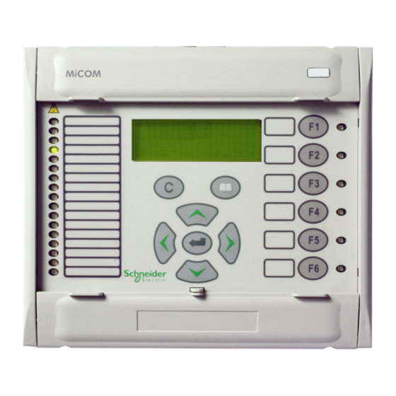
Device resetting and triggering of additional control functions used in ● testing and commissioning Control is also possible through the PC interface. This requires a suitable PC and a specific operating program. P631/EN M/R-11-C // P631-310-650... -
Page 268: Display And Keypad
(L O C: Re tur n tim e il lum in.) is set to blocked. 6.2.3 Contrast of the Display The contrast of the LC display can be adjusted by pressing 3 keys on the local control panel at the same time, as follows: P631/EN M/R-11-C // P631-310-650... -
Page 269: Short Description Of Keys
Menu Tree Level: Press the ENTER key to enter the input mode. Press the ENTER key a second time to accept the changes as entered and exit the input mode. The LED indicator labeled EDIT MODE signals that the input mode is active. 6.2.4.4 CLEAR Key P631/EN M/R-11-C // P631-310-650... - Page 270 By pressing a function key the assigned function is triggered. More details on assigning functions to function keys can be found in Section 3.6, 3-34). More details on handling function keys can be found in Section 6.8, (p. 6-10). P631/EN M/R-11-C // P631-310-650...
-
Page 271: Display Levels
(settings, signals, measured variables, etc.) and to change them, if appropriate. To access a selected event recording from either the panel level or from any other point in the menu tree, press the “READ” key: P631/EN M/R-11-C // P631-310-650... -
Page 272: Display Panels
P631 6 Local Control (HMI) Display Panels The text display of the P631 can display Measured Value Panels which are called up according to system conditions. Selected measured values are displayed on the Measured Value Panels. The system condition determines which Panel is called up (examples are the Operation Panel and the Fault Panel). -
Page 273: Menu Tree And Data Points
The value associated with the selected data point, its meaning, and its unit of measurement are displayed in the line below. P631/EN M/R-11-C // P631-310-650... -
Page 274: List Data Points
LCD, indicating that a sub-level is situated below this displayed level. The individual value elements of a list data point are found at this sub-level. In the case of a list parameter, the individual value elements are linked by operators such as “OR”. P631/EN M/R-11-C // P631-310-650... -
Page 275: Note Concerning The Step-By-Step Descriptions
LED indicator labeled Edit Mode is illuminated. The examples used here are not necessarily valid for the device type described in this manual; they merely serve to illustrate the control principles involved. P631/EN M/R-11-C // P631-310-650... -
Page 276: Configurable Function Keys
P631 6 Local Control (HMI) Configurable Function Keys 6-10 P631/EN M/R-11-C // P631-310-650... -
Page 277: Configuration Of The Function Keys F1 To Fx
1) has been entered. After the password has been entered the function key will remain active for the duration set at F _KEY: Re tur n t im e fct.k ey s. Thereafter, the function key is disabled until the password is entered again. P631/EN M/R-11-C // P631-310-650 6-11... - Page 278 Step 1 will appear. Voltage A-B prim. Step 2b This control step can be canceled at any time by 20.7 kV pressing the CLEAR key before the ENTER key is Voltage B-C prim. pressed. 20.6 kV 6-12 P631/EN M/R-11-C // P631-310-650...
- Page 279 (By default, i.e. no password required, this step does not exist and the function key is permanently effective.) P631/EN M/R-11-C // P631-310-650 6-13...
-
Page 280: Changing Between Display Levels
Press the Enter key to go from the Panel Level to the Menu Tree Level. After the set return time has elapsed (setting in menu tree: “Par/Conf/LOC”), the display will automatically switch to the Panel level if a Measured Value Panel has been configured. 6-14 P631/EN M/R-11-C // P631-310-650... -
Page 281: Control At Panel Level
The device will also show the next page of the Measured Value Panel after the set Hold-Time for Panels (LOC : H old-tim e fo r P anels, located at “Par/ Conf” in the menu tree) has elapsed. P631/EN M/R-11-C // P631-310-650 6-15... -
Page 282: Control At The Menu Tree Level
Folder Parameters Operation Events plane 1 Oper/ Folder Cyclic measurements plane 2 Oper/Cycl/ Folder Meas. operating data plane 3 Oper/Cycl/Data/ Function MAIN groups Oper/Cycl/Data/MAIN Data Date points 01.01.99 dd.mm.yy Fig. 6-3: Basic menu tree structure. 6-16 P631/EN M/R-11-C // P631-310-650... -
Page 283: Switching Between Address Mode And Plain Text Mode
To switch from address mode to plain text mode or vice 003.030 versa, press the CLEAR key and either the “left” key or the “right” key simultaneously. This can be done at any point in the menu tree. P631/EN M/R-11-C // P631-310-650 6-17... -
Page 284: Change-Enabling Function
The following example is based on the factory-set password. If the password has been changed by the user (see Section 6.11.9, (p. 6-31)), the following description will apply accordingly. 6-18 P631/EN M/R-11-C // P631-310-650... - Page 285 Once the set return time (L O C: Aut om. re tur n ti me, menu tree “Par/Conf/LOC”) has elapsed, the change-enabling function is automatically deactivated, and the P631/EN M/R-11-C // P631-310-650 6-19...
- Page 286 “off”: The value can only be changed when the protective function is ● disabled. “–”: The value can be read out but cannot be changed. ● The device is factory-set so that the protective function is disabled. 6-20 P631/EN M/R-11-C // P631-310-650...
-
Page 287: Changing Parameters
CLEAR key. The LED indicator will go out and the device will continue to operate with the old value. A further setting can be selected for a value change by pressing the keys. P631/EN M/R-11-C // P631-310-650 6-21... -
Page 288: List Parameters
Boolean equation tailored to meet user requirements. For the DNP 3.0 communication protocol, the user defines the class of a setting instead of assigning operators. The definition of a trip command shall be used here as an illustration. 6-22 P631/EN M/R-11-C // P631-310-650... - Page 289 If you wish to reject the new setting while you are still Fct.assign.trip cmd. entering it (LED indicator labeled EDIT MODE is on), #02 DIST press the CLEAR key. The LED indicator labeled EDIT Trip zone 2 MODE will be extinguished. P631/EN M/R-11-C // P631-310-650 6-23...
- Page 290 6 Local Control (HMI) 6.11.5.2 Deleting a List Parameter If MAI N: Witho ut function is assigned to a given item, then all the following items are deleted. If this occurs for item #01, everything is deleted. 6-24 P631/EN M/R-11-C // P631-310-650...
-
Page 291: Memory Readout
Press the “right” key to display the previous entry. 01.01.13 11:33 ARC Enabled USER Oper/Rec/OP_RC Step 4 Press the “up” key at any point within the operating Operat. data record. data memory to return to the entry point. ↓ P631/EN M/R-11-C // P631-310-650 6-25... - Page 292 (Yes). Number ● The signal occurred x times. Oper/Rec/MT_RC Step 5 Press the “up” key at any point within the monitoring Mon. signal record. signal memory to return to the entry point. ↓ 6-26 P631/EN M/R-11-C // P631-310-650...
- Page 293 FT_RC or the previous signal. Record. in progress Start Events/Rec/FT_RC Step 4 Press the “up” key at any point within the fault memory Fault recording 1 to return to the entry point. 01.01.13 10:00:33 ↓ P631/EN M/R-11-C // P631-310-650 6-27...
-
Page 294: Resetting
EDIT MODE is on), press the CLEAR key. The LED indicator will be extinguished, and the fault recordings remain stored unchanged in the protection unit’s memory. Any setting can be selected again for a value change by pressing the keys. 6-28 P631/EN M/R-11-C // P631-310-650... -
Page 295: Password-Protected Control Actions
The password consists of a pre-defined sequential key combination entered within a specific time interval. If the password has been changed by the user (see section “Changing the Password”), the following description will apply accordingly. P631/EN M/R-11-C // P631-310-650 6-29... - Page 296 As long as the LED indicator labeled EDIT MODE is on, Man. trip cmd. USER the control action can be terminated by pressing the Don't execute CLEAR key. The LED indicator labeled EDIT MODE will be extinguished. 6-30 P631/EN M/R-11-C // P631-310-650...
-
Page 297: Changing The Password
1, 2, 3 and 4, respectively: The password can be changed by the user at any time. The procedure for this change is described below. The starting point is the factory-set password. P631/EN M/R-11-C // P631-310-650 6-31... - Page 298 Press the enter key again. Asterisks appear in the third Password line, and a cursor (underscore) in the fourth line prompts the user to enter the new password again. Par/Conf/LOC Step 6 Re-enter the password. Password Par/Conf/LOC Password 6-32 P631/EN M/R-11-C // P631-310-650...
- Page 299 6-32), without entering anything else. This will configure the local control panel without password protection, and no control actions involving changes will be possible until the global change-enabling function has been activated (see “Change-Enabling Function”, Section 6.11.3, 6-18)). P631/EN M/R-11-C // P631-310-650 6-33...
- Page 300 “right”, “up” and “down”) at the same time and hold them down. Step 2 When this condition is detected during startup, the password is displayed. Password 1234 Step 3 After the four keys are released, startup will continue. TEST 6-34 P631/EN M/R-11-C // P631-310-650...
-
Page 301: Settings
P631 SETTINGS Parameters The P631 must be adjusted to the system and to the protected equipment by appropriate settings. This chapter gives instructions for determining the settings, which are located in the folder titled “Parameters” in the menu tree. The sequence in which the settings are listed and described in this chapter corresponds to their sequence in the menu tree. - Page 302 (active ‘low’ mode) of a voltage shall be interpreted as the logic “1” signal . General Notes on the Configuration of Function Group “Binary Output” (OUTP) The P631 has output relays for the output of binary signals. The number and connection schemes for the available binary output relays are shown in the terminal connection diagrams.
-
Page 303: Device Identification
The device identification settings are used to record the ordering information and the design version of the P631. They have no effect on the device functions. These settings should only be changed if the design version of the P631 is modified. - Page 304 Standard data models have the identifier ‘0' (factory-set default). DV ICE: F nu mber 002 124 [spacer] 9999 [spacer] The F number is the serial number of the device. The display cannot be altered. P631/EN M/R-11-C // P631-310-650...
- Page 305 DVICE : Order ext . No. 13 000 015 [spacer] DVICE : Order ext . No. 14 000 016 [spacer] DVICE : Order ext . No. 15 000 017 [spacer] DVICE : Order ext . No. 16 000 018 [spacer] P631/EN M/R-11-C // P631-310-650...
- Page 306 DV ICE: Modu l e var. slot 5 086 054 [spacer] 65535: Not fitted DV ICE: Modu l e var. slot 6 086 055 [spacer] 65535: Not fitted DV ICE: Modu l e var. slot 7 086 056 [spacer] 65535: Not fitted P631/EN M/R-11-C // P631-310-650...
- Page 307 [spacer] 65535: Not fitted [spacer] Item number of module A in this design version. DVICE : Vers ion of module A 086 190 [spacer] 27: Not fitted [spacer] Index letter specifying the version of module A. P631/EN M/R-11-C // P631-310-650...
- Page 308 DHCP. DV ICE: C ust omer ID data 1 000 040 [spacer] 0.00 0.00 99.99 DV ICE: C ust omer ID data 2 000 041 [spacer] 0.00 0.00 99.99 P631/EN M/R-11-C // P631-310-650...
- Page 309 000 048 [spacer] 9999 DVICE : Devi ce password 2 000 049 [spacer] 9999 ID code used by the operating program for identification purposes. See [spacer] description of the respective operating program for more detailed setting instructions. P631/EN M/R-11-C // P631-310-650...
- Page 310 Default Unit Logic Diagram LOC: Local HMI exi sts 221 099 Local control panel 1: Yes When set to Yes it is apparent that the device is fitted with the local control [spacer] panel (HMI). 7-10 P631/EN M/R-11-C // P631-310-650...
-
Page 311: Configuration Parameters
Operation Panel. LOC: Fc t. Over load Pan el 053 005 [spacer] 060 000: MAIN: Without function Fig. 3-4, (p. 3-7) [spacer] Definition of the values to be displayed on the Overload Panel. P631/EN M/R-11-C // P631-310-650 7-11... - Page 312 If the user does not press a key on the local control panel during this set time [spacer] period, then the backlighting of the LCD display is switched off, and any switchgear selection that might have been made is cancelled. 7-12 P631/EN M/R-11-C // P631-310-650...
- Page 313 003 181 [spacer] 1: Even Fig. 3-5, (p. 3-9) [spacer] Set the same parity that is set at the interface of the PC connected to the P631. PC : S pont an. si g. e nable 003 187 [spacer] 0: None Fig.
- Page 314 111 007 [spacer] [spacer] IP address of the Ethernet interface of the P631's processor module. This is the Ethernet interface of the processor module and can be used for special service activities, e.g. for uploading new firmware. Note: In the operating program, the complete IP address is displayed at PC: IP addr ess.
- Page 315 PC : Ti me-o ut 003 188 [spacer] Fig. 3-5, (p. 3-9) [spacer] Setting for the time to elapse after the last telegram exchange via the PC interface before activating the second communication channel of communication module A. P631/EN M/R-11-C // P631-310-650 7-15...
- Page 316 Enabling settings relevant for the COURIER protocol. [spacer] COMM1: C ommu ni cat. p rotoc ol 003 167 [spacer] 060 000: MAIN: Without function Fig. 3-6, (p. 3-11) Select the communication protocol that shall be used for the communication [spacer] interface. 7-16 P631/EN M/R-11-C // P631-310-650...
- Page 317 Fig. 3-9, (p. 3-14) Fig. 3-10, (p. 3-15) Fig. 3-11, (p. 3-16) Fig. 3-12, (p. 3-17) Set the same parity that is set at the interface of the control system connected [spacer] to the P631. P631/EN M/R-11-C // P631-310-650 7-17...
- Page 318 Fig. 3-11, (p. 3-16) Fig. 3-12, (p. 3-17) [spacer] The P631 monitors telegram transmission to make sure that no excessive pause occurs within a telegram. This monitoring function can be disabled if it is not required. Note: This setting is only necessary for modem transmission.
- Page 319 Fig. 3-7, (p. 3-12) Fig. 3-8, (p. 3-13) Fig. 3-9, (p. 3-14) Enable for the transmission of spontaneous signals via the communication [spacer] interface. Note: This setting is hidden unless an IEC 870-5 protocol is enabled. P631/EN M/R-11-C // P631-310-650 7-19...
- Page 320 Fig. 3-9, (p. 3-14) [spacer] The telegram is transmitted if a measured value differs by the set delta quantity from the last measured value transmitted. Note: This setting is hidden unless an IEC 870-5 protocol is enabled. 7-20 P631/EN M/R-11-C // P631-310-650...
- Page 321 Fig. 3-9, (p. 3-14) [spacer] A continuous or background general scan means that the P631 transmits all settings, signals, and monitoring signals through the communication interface during slow periods when there is not much activity. This ensures that there will be data consistency with a connected control system.
- Page 322 Fig. 3-8, (p. 3-13) [spacer] Setting specifying whether telegram structure 2 shall be converted as a single signal or double signal. Note: This setting is hidden unless the IEC 870-5-101 protocol is set. “ASDU”: Application Service Data Unit 7-22 P631/EN M/R-11-C // P631-310-650...
- Page 323 Assignment is made in the order of selection. This means that the first measured value is given the register no. 30301, the second the register no. 30302, etc. Note: This setting is hidden unless the MODBUS protocol is enabled. P631/EN M/R-11-C // P631-310-650 7-23...
- Page 324 0.10 0.05 2.54 Fig. 3-11, (p. 3-16) [spacer] Setting for the time period within which the master must acknowledge at the link layer. Note: This setting is hidden unless the DNP 3.0 protocol is enabled. 7-24 P631/EN M/R-11-C // P631-310-650...
- Page 325 Selection of data points and data classes for object 40 – analog outputs. [spacer] Assignment of indices is made in the order of selection, beginning with 0. Note: This setting is hidden unless the DNP 3.0 protocol is enabled. P631/EN M/R-11-C // P631-310-650 7-25...
- Page 326 COMM1: Del ta t ( COURIE R) 103 046 [spacer] Fig. 3-12, (p. 3-17) [spacer] Cycle time at the conclusion of which the selected measured values are again transmitted. Note: This setting is hidden unless the COURIER protocol is enabled. 7-26 P631/EN M/R-11-C // P631-310-650...
- Page 327 1: Yes Fig. 3-14, (p. 3-19) [spacer] The P631 monitors telegram transmission to make sure that no excessive pause occurs within a telegram. This monitoring function can be disabled if it is not required. Note: This setting is only necessary for modem transmission.
- Page 328 COMM2: Del ta V 103 050 [spacer] 15.0 %Vnom Fig. 3-14, (p. 3-19) A measured voltage value is transmitted via the communication interface if it [spacer] differs by the set delta quantity from the last measured value transmitted. 7-28 P631/EN M/R-11-C // P631-310-650...
- Page 329 [spacer] Fig. 3-14, (p. 3-19) All measured values are transmitted again via the communication interface after [spacer] this time period has elapsed – provided that transmission has not been triggered by the other delta conditions. P631/EN M/R-11-C // P631-310-650 7-29...
- Page 330 Setting is carried out with the IED Configurator. I EC: Inac t. C onf ig. Ver s. 104 048 [spacer] Version number of the inactive configuration bank. [spacer] Setting is carried out with the IED Configurator. 7-30 P631/EN M/R-11-C // P631-310-650...
- Page 331 IEC: SNT P s erv er 2 I P 104 210 [spacer] IP address of the backup server used for clock synchronization. [spacer] Note: This is an information parameter ('read only') and its value is set from the "IED Configurator". P631/EN M/R-11-C // P631-310-650 7-31...
- Page 332 104 225 [spacer] 5: Last I EC: Day l.sav.t i me e n d d 104 226 [spacer] 7: Sunday I EC: Day l.sav.t i me e n d m 104 227 [spacer] 10: October 7-32 P631/EN M/R-11-C // P631-310-650...
- Page 333 [spacer] This parameter defines the date and time of day for the clock changeover from daylight saving time to standard time. The setting is similar to that for the clock changeover to daylight saving time. P631/EN M/R-11-C // P631-310-650 7-33...
- Page 334 GOOS E: Ou tpu t 11 f ct .ass ig. 106 031 [spacer] 060 000: MAIN: Without function GOOS E: Ou tpu t 12 f ct .ass ig. 106 033 [spacer] 060 000: MAIN: Without function 7-34 P631/EN M/R-11-C // P631-310-650...
- Page 335 060 000: MAIN: Without function GOOSE : Out pu t 30 fc t.a ssig. 106 069 [spacer] 060 000: MAIN: Without function GOOSE : Out pu t 31 fc t.a ssig. 106 071 [spacer] 060 000: MAIN: Without function P631/EN M/R-11-C // P631-310-650 7-35...
- Page 336 061 000: MAIN: Without function GOOS E: In put 15 f ct. assig. 107 146 [spacer] 061 000: MAIN: Without function GOOS E: In put 16 f ct. assig. 107 156 [spacer] 061 000: MAIN: Without function 7-36 P631/EN M/R-11-C // P631-310-650...
- Page 337 GosGGIO1/Pos32.stVal) to a binary logical state signal on the device so that they can be processed further by the protection, control or logic functions. Signals configured here contain the received and pre-processed state of data attributes configured for GOOSE receipt. P631/EN M/R-11-C // P631-310-650 7-37...
- Page 338 Promiscuous and after all GSSE sending devices have logged- on, only messages with the MAC addresses of IEDs, that have logged-on successfully, are read and processed. GS S E: Ou tput 1 bi t pair 104 101 [spacer] 0: No selection 7-38 P631/EN M/R-11-C // P631-310-650...
- Page 339 GS SE: Outpu t 18 bi t pair 104 152 [spacer] 0: No selection GS SE: Outpu t 19 bi t pair 104 155 [spacer] 0: No selection GS SE: Outpu t 20 bi t pair 104 158 [spacer] 0: No selection P631/EN M/R-11-C // P631-310-650 7-39...
- Page 340 060 000: MAIN: Without function GS S E: Ou tput 4 f ct.a ssig. 104 111 [spacer] 060 000: MAIN: Without function GS S E: Ou tput 5 f ct.a ssig. 104 114 [spacer] 060 000: MAIN: Without function 7-40 P631/EN M/R-11-C // P631-310-650...
- Page 341 060 000: MAIN: Without function GS SE: Outpu t 23 fct .ass ig. 104 168 [spacer] 060 000: MAIN: Without function GS SE: Outpu t 24 fct .ass ig. 104 171 [spacer] 060 000: MAIN: Without function P631/EN M/R-11-C // P631-310-650 7-41...
- Page 342 105 031 [spacer] 0: No selection GS S E: Inp ut 8 bi t pair 105 036 [spacer] 0: No selection GS S E: Inp ut 9 bi t pair 105 041 [spacer] 0: No selection 7-42 P631/EN M/R-11-C // P631-310-650...
- Page 343 0: No selection GS SE: In pu t 2 7 bi t pair 105 131 [spacer] 0: No selection GS SE: In pu t 2 8 bi t pair 105 136 [spacer] 0: No selection P631/EN M/R-11-C // P631-310-650 7-43...
- Page 344 1: Remote IED GS S E: Inp ut 12 IE D na me 105 057 [spacer] 1: Remote IED GS S E: Inp ut 13 IE D na me 105 062 [spacer] 1: Remote IED 7-44 P631/EN M/R-11-C // P631-310-650...
- Page 345 1: Remote IED GS SE: In pu t 3 0 IED n ame 105 147 [spacer] 1: Remote IED GS SE: In pu t 3 1 IED n ame 105 152 [spacer] 1: Remote IED P631/EN M/R-11-C // P631-310-650 7-45...
- Page 346 GS S E: Inp ut 15 defaul t 105 073 [spacer] 0: 0 GS S E: Inp ut 16 defaul t 105 078 [spacer] 0: 0 GS S E: Inp ut 17 defaul t 105 083 [spacer] 0: 0 7-46 P631/EN M/R-11-C // P631-310-650...
- Page 347 GS SE: In pu t 1 fct .assig. 105 004 [spacer] 061 000: MAIN: Without function GS SE: In pu t 2 fct .assig. 105 009 [spacer] 061 000: MAIN: Without function P631/EN M/R-11-C // P631-310-650 7-47...
- Page 348 061 000: MAIN: Without function GS S E: Inp ut 20 fct.assi g . 105 099 [spacer] 061 000: MAIN: Without function GS S E: Inp ut 21 fct.assi g . 105 104 [spacer] 061 000: MAIN: Without function 7-48 P631/EN M/R-11-C // P631-310-650...
- Page 349 IRIGB : Gener al en abl e U SE R 023 200 [spacer] 0: No Fig. 3-20, (p. 3-33) [spacer] Disabling or enabling the IRIG-B interface. P631/EN M/R-11-C // P631-310-650 7-49...
- Page 350 F_KE Y: Oper ati n g mode F2 080 133 [spacer] 1: Key F_KE Y: Oper ati n g mode F3 080 134 [spacer] 1: Key F_KE Y: Oper ati n g mode F4 080 135 [spacer] 1: Key 7-50 P631/EN M/R-11-C // P631-310-650...
- Page 351 F_ KEY: Re t ur n time fct. keys 003 037 [spacer] 60000 [spacer] Once the password has been entered, the function keys remain active for no longer than this time. Thereafter, the function keys are disabled until the password is entered again. P631/EN M/R-11-C // P631-310-650 7-51...
- Page 352 I NP: Oper. m ode U 703 152 116 [spacer] 1: Active "high" I NP: Oper. m ode U 704 152 119 [spacer] 1: Active "high" I NP: Oper. m ode U 705 152 122 [spacer] 1: Active "high" 7-52 P631/EN M/R-11-C // P631-310-650...
- Page 353 1: Active "high" INP: Oper. mode U 90 3 152 152 [spacer] 1: Active "high" INP: Oper. mode U 90 4 152 155 [spacer] 1: Active "high" [spacer] Selection of operating mode for binary signal inputs. P631/EN M/R-11-C // P631-310-650 7-53...
- Page 354 0.000 0.200 IDC,nom Fig. 3-26, (p. 3-41) Setting for the minimum current that must flow in order for the P631 to display a [spacer] measured value > 0 (zero suppression). ME AS I: I DC < ope n ci rcuit...
- Page 355 MEA SI: I DC,l i n 7 037 163 [spacer] Blocked 0.000 1.200 IDC,nom Fig. 3-26, (p. 3-41) MEA SI: I DC,l i n 8 037 165 [spacer] Blocked 0.000 1.200 IDC,nom Fig. 3-26, (p. 3-41) P631/EN M/R-11-C // P631-310-650 7-55...
- Page 356 Setting for the scaled value of IDC,lin1. ME AS I: S cal ed v al .IDC ,l in20 037 193 [spacer] 1200 -32768 32767 Fig. 3-27, (p. 3-42) [spacer] Setting for the scaled value of IDC,lin20. 7-56 P631/EN M/R-11-C // P631-310-650...
- Page 357 OUTP : Oper . mode K 7 02 150 149 [spacer] 1: ES updating OUTP : Oper . mode K 7 03 150 152 [spacer] 1: ES updating OUTP : Oper . mode K 7 04 150 155 [spacer] 1: ES updating P631/EN M/R-11-C // P631-310-650 7-57...
- Page 358 OUT P: Oper. m ode K 9 07 150 212 [spacer] 1: ES updating OUT P: Oper. m ode K 9 08 150 215 [spacer] 1: ES updating Selection of operating mode for output relays. [spacer] 7-58 P631/EN M/R-11-C // P631-310-650...
- Page 359 037 140 [spacer] 0.000 0.000 1.000 MEA SO: S cal ed max . val. BCD 037 141 [spacer] 1.000 0.000 1.000 MEA SO: B CD- Out mi n . va lu e 037 142 [spacer] P631/EN M/R-11-C // P631-310-650 7-59...
- Page 360 ME AS O: Scal ed max. v al. A- 1 037 106 [spacer] 1.000 0.000 1.000 Fig. 3-36, (p. 3-57) ME AS O: Scal ed mi n. v al. A- 2 037 110 [spacer] 0.000 0.000 1.000 7-60 P631/EN M/R-11-C // P631-310-650...
- Page 361 0.00 20.00 Fig. 3-36, (p. 3-57) MEA SO: AnOu t min. v al. A-2 037 113 [spacer] 0.00 0.00 20.00 MEA SO: AnOu t kne e point A- 2 037 114 [spacer] Blocked 0.00 20.00 P631/EN M/R-11-C // P631-310-650 7-61...
- Page 362 0.00 100.00 ME AS O: Ou tpu t va lu e 3 037 122 [spacer] 0.00 0.00 100.00 Measured values of external devices, which must be scaled to 0 to 100%, can be [spacer] issued. 7-62 P631/EN M/R-11-C // P631-310-650...
- Page 363 060 000: MAIN: Without function LED: F ct.assi g. H 9 re d 085 022 [spacer] 060 000: MAIN: Without function LED: F ct.assi g. H 9 gr ee n 085 072 [spacer] 060 000: MAIN: Without function P631/EN M/R-11-C // P631-310-650 7-63...
- Page 364 060 000: MAIN: Without function LE D: F ct .as sig. H 19 green 085 164 [spacer] 060 000: MAIN: Without function LE D: F ct .as sig. H 20 red 085 137 [spacer] 060 000: MAIN: Without function 7-64 P631/EN M/R-11-C // P631-310-650...
- Page 365 LED: O pe rat ing mode H 5 085 011 [spacer] 1: ES updating LED: O pe rat ing mode H 6 085 014 [spacer] 1: ES updating LED: O pe rat ing mode H 7 085 017 [spacer] 1: ES updating P631/EN M/R-11-C // P631-310-650 7-65...
- Page 366 1: ES updating [spacer] Selection of operating mode for LED indicators. LE D: O pe ratin g mod e H 17 085 183 [spacer] 1: ES updating [spacer] The operating mode ES updating is permanently assigned. 7-66 P631/EN M/R-11-C // P631-310-650...
- Page 367 FT _RC: Rec. anal og cha nn. 6 035 165 [spacer] 70: Current IB,b FT _RC: Rec. anal og cha nn. 7 035 166 [spacer] 71: Current IC,b [spacer] The user specifies the channel on which each physical variable is recorded. P631/EN M/R-11-C // P631-310-650 7-67...
- Page 368 Thermal overload protection 0: Without [spacer] Cancelling function group THR_1 or including it in the configuration. If the function group is cancelled, then all associated settings and signals are hidden, with the exception of this setting. 7-68 P631/EN M/R-11-C // P631-310-650...
- Page 369 0: Without [spacer] Cancelling function group LIMIT or including it in the configuration. If the function group is cancelled from the configuration, then all associated settings and signals are hidden, with the exception of this setting. P631/EN M/R-11-C // P631-310-650 7-69...
- Page 370 Programmable Logic LOG_2: Fu nc tion gr oup L OG _2 056 089 0: Without Cancelling function group LOG_2 (“Logic 2”) or including it in the configuration. [spacer] If the function group is cancelled from the configuration, then all associated settings and signals are hidden. 7-70 P631/EN M/R-11-C // P631-310-650...
-
Page 371: Function Parameters
0: No Fig. 3-7, (p. 3-12) Fig. 3-8, (p. 3-13) Fig. 3-9, (p. 3-14) [spacer] When signal and measured value blocking user is activated, no signals or measured data are transmitted through communication interface COMM1. P631/EN M/R-11-C // P631-310-650 7-71... - Page 372 Default Unit Logic Diagram OU TP : Outp.rel .bl ock USE R 021 014 Binary and analog output 0: No Fig. 3-29, (p. 3-45) When this blocking is activated, all output relays are blocked. [spacer] 7-72 P631/EN M/R-11-C // P631-310-650...
- Page 373 Setting for the nominal current of the device for the measurement of the phase currents of ends a or b. This also corresponds to the nominal device current. MAIN: C onn .meas.cir c. IP,a 010 140 [spacer] 1: Standard Fig. 3-39, (p. 3-62) Fig. 3-40, (p. 3-63) P631/EN M/R-11-C // P631-310-650 7-73...
- Page 374 0.000 0.200 Inom [spacer] Setting for a minimum current that must be exceeded in order for the P631 to display the negative-sequence (positive-sequence) current as measured operating data. MA IN : Meas. val ue r e l. IN 011 031 [spacer] 0.000...
- Page 375 Assignment of signals that trigger trip command 4. MAIN: Mi n.dur . tri p cmd. 1 021 003 [spacer] 0.25 0.10 10.00 Fig. 3-55, (p. 3-81) Setting for the minimum duration of trip command 1. [spacer] P631/EN M/R-11-C // P631-310-650 7-75...
- Page 376 MA IN : Fct. assi gn. fau lt 021 031 [spacer] 060 000: MAIN: Without function Fig. 3-52, (p. 3-79) [spacer] Selection of the signals to be signaled as Blocked/Faulty in addition to the messages that always result in the message Blocked/Faulty. 7-76 P631/EN M/R-11-C // P631-310-650...
- Page 377 This setting defines the duration (in hours) for which a device-internal fault is [spacer] stored, so that a decision may be taken between an automatic warm restart and an automatic device blocking. (Setting to Blocked may be considered the same as unlimited storage.) P631/EN M/R-11-C // P631-310-650 7-77...
- Page 378 018 009 Main function Blocked 0.00 100.00 Fig. 3-49, (p. 3-76) Setting for the hold time of the “dynamic parameters”. During this period, the [spacer] “dynamic” thresholds are active in place of the “normal” thresholds. 7-78 P631/EN M/R-11-C // P631-310-650...
- Page 379 019 023 [spacer] Not measured 0.000 50.000 Fig. 3-78, (p. 3-111) [spacer] Display of the reference current calculated by the P631 for end a. DIFF: Re f . cur r. Iref, b 019 024 [spacer] Not measured 0.000 50.000 Fig. 3-78, (p. 3-111) [spacer] Display of the reference current calculated by the P631 for end b.
- Page 380 I DMT2: S e le ct. me as. i npu t 019 116 [spacer] 1: End b [spacer] Selection of the measuring input that provides the measured variables monitored by the inverse-time overcurrent protection function. 7-80 P631/EN M/R-11-C // P631-310-650...
- Page 381 Address Default Unit Logic Diagram CT S: Gen er al e nabl e USE R 031 085 Current transformer supervision 0: No Fig. 3-116, (p. 3-151) [spacer] Enabling or disabling the current transformer supervision function. P631/EN M/R-11-C // P631-310-650 7-81...
- Page 382 MC M_1 : Sel ect . meas. i npu t 031 150 [spacer] 0: End a MC M_2 : Sel ect . meas. i npu t 031 151 [spacer] 1: End b [spacer] Assigning measuring-circuit monitoring functions to ends a and b. 7-82 P631/EN M/R-11-C // P631-310-650...
- Page 383 Fig. 3-130, (p. 3-163) Fig. 3-134, (p. 3-165) Fig. 3-135, (p. 3-166) CB F_2 : I< 022 215 [spacer] 1.00 0.05 20.00 Inom Setting for the threshold to detect a break in current flow. [spacer] P631/EN M/R-11-C // P631-310-650 7-83...
- Page 384 022 224 [spacer] 0.25 0.10 10.00 Setting the 2nd timer stage for minimum duration of trip command. [spacer] CBF _1: Latc hi ng tr ip cm d.t1 022 169 [spacer] 0: No Fig. 3-132, (p. 3-164) 7-84 P631/EN M/R-11-C // P631-310-650...
- Page 385 Fig. 3-135, (p. 3-166) CB F_2 : Del ay /C B syn c. super v 022 218 [spacer] Blocked 0.00 100.00 Setting for the time delay to bridge circuit breaker operate times during CB [spacer] synchronization supervision. P631/EN M/R-11-C // P631-310-650 7-85...
- Page 386 Fig. 3-136, (p. 3-168) [spacer] Setting for the operate delay of undercurrent stage IDC,lin<<. LIMIT : T > 014 100 [spacer] °C Fig. 3-137, (p. 3-169) [spacer] Setting for the operate value of temperature monitoring T>. 7-86 P631/EN M/R-11-C // P631-310-650...
- Page 387 Fig. 3-137, (p. 3-169) [spacer] Setting for the operate delay of temperature monitoring T<. LIMIT : tT< < 014 108 [spacer] Blocked 1000 Fig. 3-137, (p. 3-169) [spacer] Setting for the operate delay of temperature monitoring T<<. P631/EN M/R-11-C // P631-310-650 7-87...
- Page 388 Setting for the operate delay of I>>. LIM_1: I< 015 118 [spacer] 0.10 0.00 4.00 Inom Fig. 3-139, (p. 3-171) LIM_2: I< 016 118 [spacer] 0.10 0.00 4.00 Inom [spacer] Setting for the operate value of I<. 7-88 P631/EN M/R-11-C // P631-310-650...
- Page 389 [spacer] Setting for the operate delay of I<. [spacer] LIM_ 1: tI<< 015 123 [spacer] Blocked Fig. 3-139, (p. 3-171) LIM_ 2: tI<< 016 123 [spacer] Blocked [spacer] Setting for the operate delay of I<<. P631/EN M/R-11-C // P631-310-650 7-89...
- Page 390 060 000: MAIN: Without function LOGIC: Fct.assi gn m. ou tp. 7 030 024 [spacer] 060 000: MAIN: Without function LOGIC: Fct.assi gn m. ou tp. 8 030 028 [spacer] 060 000: MAIN: Without function 7-90 P631/EN M/R-11-C // P631-310-650...
- Page 391 060 000: MAIN: Without function LOGIC : Fct .assi gn m. ou tp. 26 031 000 [spacer] 060 000: MAIN: Without function LOGIC : Fct .assi gn m. ou tp. 27 031 004 [spacer] 060 000: MAIN: Without function P631/EN M/R-11-C // P631-310-650 7-91...
- Page 392 030 041 [spacer] 0: Without timer stage LOGIC: Op. mode t ou tput 12 030 045 [spacer] 0: Without timer stage LOGIC: Op. mode t ou tput 13 030 049 [spacer] 0: Without timer stage 7-92 P631/EN M/R-11-C // P631-310-650...
- Page 393 031 013 [spacer] 0: Without timer stage LOGIC : Op. mode t output 30 031 017 [spacer] 0: Without timer stage LOGIC : Op. mode t output 31 031 021 [spacer] 0: Without timer stage P631/EN M/R-11-C // P631-310-650 7-93...
- Page 394 LOGIC: Ti me t1 ou tpu t 15 030 058 [spacer] 0.00 0.00 600.00 LOGIC: Ti me t1 ou tpu t 16 030 062 [spacer] 0.00 0.00 600.00 LOGIC: Ti me t1 ou tpu t 17 030 066 [spacer] 0.00 0.00 600.00 7-94 P631/EN M/R-11-C // P631-310-650...
- Page 395 Fig. 3-141, (p. 3-174) LOGIC : Ti me t 2 ou tp ut 2 030 007 [spacer] 0.00 0.00 600.00 LOGIC : Ti me t 2 ou tp ut 3 030 011 [spacer] 0.00 0.00 600.00 P631/EN M/R-11-C // P631-310-650 7-95...
- Page 396 LOGIC: Ti me t2 ou tpu t 20 030 079 [spacer] 0.00 0.00 600.00 LOGIC: Ti me t2 ou tpu t 21 030 083 [spacer] 0.00 0.00 600.00 LOGIC: Ti me t2 ou tpu t 22 030 087 [spacer] 0.00 0.00 600.00 7-96 P631/EN M/R-11-C // P631-310-650...
- Page 397 061 000: MAIN: Without function LOGIC : S ig .assig. outp. 7 044 012 [spacer] 061 000: MAIN: Without function LOGIC : S ig .assig. outp. 8 044 014 [spacer] 061 000: MAIN: Without function P631/EN M/R-11-C // P631-310-650 7-97...
- Page 398 061 000: MAIN: Without function LOGIC: Si g.assi g. ou tp. 26 044 050 [spacer] 061 000: MAIN: Without function LOGIC: Si g.assi g. ou tp. 27 044 052 [spacer] 061 000: MAIN: Without function 7-98 P631/EN M/R-11-C // P631-310-650...
- Page 399 061 000: MAIN: Without function LOGIC : S ig .assig.outp .1 2(t) 044 023 [spacer] 061 000: MAIN: Without function LOGIC : S ig .assig.outp .1 3(t) 044 025 [spacer] 061 000: MAIN: Without function P631/EN M/R-11-C // P631-310-650 7-99...
- Page 400 LOGIC: Si g.assi g.outp.2 9(t) 044 057 [spacer] 061 000: MAIN: Without function LOGIC: Si g.assi g.outp.3 0(t) 044 059 [spacer] 061 000: MAIN: Without function LOGIC: Si g.assi g.outp.3 1(t) 044 061 [spacer] 061 000: MAIN: Without function 7-100 P631/EN M/R-11-C // P631-310-650...
- Page 401 Unit Logic Diagram LOGIC : S ig .assig.outp. 32(t) 044 063 [spacer] 061 000: MAIN: Without function [spacer] These settings assign the function of a binary input signal to the output of the logic equation. P631/EN M/R-11-C // P631-310-650 7-101...
- Page 402 LOG_2: T im e t2 ou tp ut 1 050 003 [spacer] 60000 Fig. 3-142, (p. 3-175) LOG_2: T im e t2 ou tp ut 2 050 007 [spacer] 60000 LOG_2: T im e t2 ou tp ut 3 050 011 [spacer] 60000 7-102 P631/EN M/R-11-C // P631-310-650...
- Page 403 061 000: MAIN: Without function LOG_2: S ig .as sig.ou tp. 4(t) 064 007 [spacer] 061 000: MAIN: Without function [spacer] These settings assign the function of a binary input signal to the output of the logic equation. P631/EN M/R-11-C // P631-310-650 7-103...
- Page 404 Phases to be reversed (A-B swapped, A-B swapped or A-B swapped) may be set separately for each end. At the same time the display MAIN : Ph as e r e ve rsa l ac tiv will be triggered unless the setting is No swap. 7-104 P631/EN M/R-11-C // P631-310-650...
- Page 405 Threshold value of the differential current for deactivation of the inrush stabilization function (harmonic restraint) and of the overfluxing restraint. Note: If the threshold is set too high, it is possible for the P631 not to trip in the presence of internal faults with transformer saturation.
- Page 406 Note: If the threshold is set too low, the P631 can trip in the presence of external faults with transformer saturation. DIF F: Idif f>( CTS ) PS x...
- Page 407 The time-delay of the differential protection trip signal can be set here. DIFF: H yst. e ffect ive PSx 072 006 073 006 074 006 075 006 [spacer] 1: Yes [spacer] The hysteresis of the pick-up characteristics may be disabled or enabled. P631/EN M/R-11-C // P631-310-650 7-107...
- Page 408 079 051 [spacer] 1.00 0.10 30.00 Inom Fig. 3-92, (p. 3-125) DT OC2: I> PS x 076 071 077 071 078 071 079 071 [spacer] 1.00 0.10 30.00 Inom Setting for operate value I>. [spacer] 7-108 P631/EN M/R-11-C // P631-310-650...
- Page 409 078 077 079 077 [spacer] 1.00 0.00 100.00 Setting for operate delay I>. [spacer] DTOC 1: tI>> P S x 076 058 077 058 078 058 079 058 [spacer] 0.50 0.00 100.00 Fig. 3-92, (p. 3-125) P631/EN M/R-11-C // P631-310-650 7-109...
- Page 410 This operate value is effective only while the timer stage MAIN : Ho ld tim e d yn.p aram. is elapsing. DT OC1: In eg>> dyn ami c PSx 076 201 077 201 078 201 079 201 [spacer] 1.00 0.10 8.00 Inom Fig. 3-93, (p. 3-127) 7-110 P631/EN M/R-11-C // P631-310-650...
- Page 411 079 164 [spacer] 0.25 0.10 8.00 Inom [spacer] Setting for operate value IN>. DTOC 1: IN>> P S x 076 055 077 055 078 055 079 055 [spacer] Blocked 0.10 8.00 Inom Fig. 3-94, (p. 3-129) P631/EN M/R-11-C // P631-310-650 7-111...
- Page 412 [spacer] 0.50 0.00 100.00 Fig. 3-94, (p. 3-129) DT OC2: tIN>> P Sx 076 171 077 171 078 171 079 171 [spacer] 0.50 0.00 100.00 [spacer] Setting for the operate delay of the IN>> stage. 7-112 P631/EN M/R-11-C // P631-310-650...
- Page 413 0.50 0.00 100.00 Fig. 3-94, (p. 3-129) DTOC 2: tIN >>> PS x 076 172 077 172 078 172 079 172 [spacer] 0.50 0.00 100.00 [spacer] Setting for the operate delay of the IN>>> stage. P631/EN M/R-11-C // P631-310-650 7-113...
- Page 414 4.00 Inom Fig. 3-103, (p. 3-138) I DMT2: Ire f ,P PS x 081 171 082 171 083 171 084 171 [spacer] 1.00 0.10 4.00 Inom [spacer] Setting for the reference current (phase current system). 7-114 P631/EN M/R-11-C // P631-310-650...
- Page 415 1: Without delay Setting for the reset characteristic (phase current system). [spacer] IDMT 1: Ire f,n eg PS x 081 111 082 111 083 111 084 111 [spacer] Blocked 0.01 0.80 Inom Fig. 3-104, (p. 3-140) P631/EN M/R-11-C // P631-310-650 7-115...
- Page 416 Setting for the hold time for storing the starting time once the starting has [spacer] dropped out (negative-sequence current system). I DMT1: Rel eas e n eg P Sx 081 116 082 116 083 116 084 116 [spacer] 1: Without delay Fig. 3-104, (p. 3-140) 7-116 P631/EN M/R-11-C // P631-310-650...
- Page 417 IDMT 2: Hol d t i me N P Sx 081 185 082 185 083 185 084 185 [spacer] 0.00 0.00 600.00 [spacer] Setting for the hold time for storing the starting time once the starting has dropped out (residual current system). P631/EN M/R-11-C // P631-310-650 7-117...
- Page 418 1: Without delay Fig. 3-105, (p. 3-142) I DMT2: Rel eas e N P Sx 081 186 082 186 083 186 084 186 [spacer] 1: Without delay [spacer] Setting for the reset characteristic (residual current system). 7-118 P631/EN M/R-11-C // P631-310-650...
- Page 419 Select the mode of the coolant temperature acquisition. Select from: No data acquisition. A default temperature value is used instead, ● data acquisition via the PT 100 input, ● data acquisition via the 20 mA input. ● P631/EN M/R-11-C // P631-310-650 7-119...
- Page 420 083 085 084 085 [spacer] 30.0 1000.0 Fig. 3-114, (p. 3-149) [spacer] A warning will be given in advance of the trip. The time difference between the warning time and the trip time is set here. 7-120 P631/EN M/R-11-C // P631-310-650...
- Page 421 CT S: t( L at ch ) P S x 001 130 001 131 001 132 001 133 [spacer] 1.00 0.00 10.00 Fig. 3-121, (p. 3-155) Fig. 3-122, (p. 3-155) [spacer] Setting for the latching time-delay. P631/EN M/R-11-C // P631-310-650 7-121...
- Page 422 . en d, MA IN : K2 00 fail. c md. star t, MAIN : D EV op .tim e exceede d) are issued when the monitoring time-delay has expired and the direction control contacts will remain closed. (Note: This behavior still bears the danger of an undefined switch position!) 7-122 P631/EN M/R-11-C // P631-310-650...
-
Page 423: Information And Control Functions
INFORMATION AND CONTROL FUNCTIONS Operation The P631 generates a large number of signals, processes binary input signals, and acquires measured data during fault-free operation of the protected object as well as fault-related data. A number of counters are available for statistical purposes. -
Page 424: Cyclic Values
ME AS I: T emperatu re Tmax 004 233 [spacer] Not measured -40.0 215.0 °C Fig. 3-28, (p. 3-43) [spacer] Display of the maximum temperature measured at the “PT 100” temperature input on the analog p/c board. P631/EN M/R-11-C // P631-310-650... - Page 425 0.00 0.00 20.00 Fig. 3-36, (p. 3-57) MEA SO: Curr en t A-2 005 099 [spacer] 0.00 0.00 20.00 Display of the current on the analog measured data output (A1: channel 1; A2: [spacer] channel 2). P631/EN M/R-11-C // P631-310-650...
- Page 426 Display of the delayed stored maximum phase current of end b as a primary [spacer] quantity. MA IN : Curr. IP,mi n ,a pr im. 005 104 [spacer] Not measured 25000 Fig. 3-44, (p. 3-70) [spacer] Display of the minimum phase current of end a as a primary quantity. P631/EN M/R-11-C // P631-310-650...
- Page 427 MAIN: C urren t Ipos b pr im. 005 134 [spacer] Not measured 25000 [spacer] Display of the positive-sequence current of the respective end as a primary quantity. MAIN: C urren t IN,a pr im. 005 121 [spacer] Not measured 25000 P631/EN M/R-11-C // P631-310-650...
- Page 428 [spacer] Not measured 25000 [spacer] Display of the residual current calculated by the P631 from the sum of the phase currents (of the respective end) as a primary quantity. MA IN : Curr. IP,ma x,a p.u . 005 111 [spacer] Not measured 0.000...
- Page 429 0.000 25.000 Inom [spacer] Display of the residual current calculated by the P631 from the sum of the phase currents of the respective end, referred to I MAIN: A ngl e phi AB , en d a 005 089 [spacer] Not measured -180.0...
- Page 430 MA IN : Angl e ph i C, e n d a-b 007 090 [spacer] Not measured -180.0 180.0 ° Fig. 3-47, (p. 3-73) Display of the phase shift between ends a and b for phase C. [spacer] P631/EN M/R-11-C // P631-310-650...
- Page 431 DIFF: Re strai n . cu rr ent 3 007 081 [spacer] Not measured 0.000 40.000 Iref Fig. 3-89, (p. 3-122) [spacer] Display of the restraining current for measuring system 1, 2 or 3, respectively, referred to I P631/EN M/R-11-C // P631-310-650...
- Page 432 Display of the temperature of the protected object referred to 100°C. THRM1: Coo lant temp. p .u. 1 004 206 [spacer] Not measured -0.40 2.00 100°C Fig. 3-114, (p. 3-149) [spacer] Display of the coolant temperature of the protected object referred to 100°C. 8-10 P631/EN M/R-11-C // P631-310-650...
- Page 433 The additional reserve amounts to 0 in this case. P631/EN M/R-11-C // P631-310-650 8-11...
- Page 434 GOOS E: Ou tpu t 15 st ate 106 038 [spacer] 0: 0 GOOS E: Ou tpu t 16 st ate 106 040 [spacer] 0: 0 GOOS E: Ou tpu t 17 st ate 106 042 [spacer] 0: 0 8-12 P631/EN M/R-11-C // P631-310-650...
- Page 435 GOOSE : Inpu t 1 stat e 106 200 [spacer] 0: 0 GOOSE : Inpu t 2 stat e 106 201 [spacer] 0: 0 GOOSE : Inpu t 3 stat e 106 202 [spacer] 0: 0 P631/EN M/R-11-C // P631-310-650 8-13...
- Page 436 GOOS E: In put 20 st ate 106 219 [spacer] 0: 0 GOOS E: In put 21 st ate 106 220 [spacer] 0: 0 GOOS E: In put 22 st ate 106 221 [spacer] 0: 0 8-14 P631/EN M/R-11-C // P631-310-650...
- Page 437 0: 0 GOOSE : Inpu t 31 stat e 106 230 [spacer] 0: 0 GOOSE : Inpu t 32 stat e 106 231 [spacer] 0: 0 Display of the virtual binary GOOSE input state. [spacer] P631/EN M/R-11-C // P631-310-650 8-15...
- Page 438 GS S E: Ou tput 16 state 104 145 [spacer] 0: 0 GS S E: Ou tput 17 state 104 148 [spacer] 0: 0 GS S E: Ou tput 18 state 104 151 [spacer] 0: 0 8-16 P631/EN M/R-11-C // P631-310-650...
- Page 439 GS SE: In pu t 2 stat e 105 005 [spacer] 0: 0 GS SE: In pu t 3 stat e 105 010 [spacer] 0: 0 GS SE: In pu t 4 stat e 105 015 [spacer] 0: 0 P631/EN M/R-11-C // P631-310-650 8-17...
- Page 440 GS S E: Inp ut 21 stat e 105 100 [spacer] 0: 0 GS S E: Inp ut 22 stat e 105 105 [spacer] 0: 0 GS S E: Inp ut 23 stat e 105 110 [spacer] 0: 0 8-18 P631/EN M/R-11-C // P631-310-650...
- Page 441 GS SE: In pu t 3 1 st ate 105 150 [spacer] 0: 0 GS SE: In pu t 3 2 st ate 105 155 [spacer] 0: 0 [spacer] Display of the virtual binary GSSE input state. P631/EN M/R-11-C // P631-310-650 8-19...
- Page 442 The state of the function keys is displayed as follows: Without function: No functions are assigned to the function key. ● "Off": The function key is in the “Off” position. ● "On": The function key is in the “On” position. ● 8-20 P631/EN M/R-11-C // P631-310-650...
- Page 443 The state of the binary signal inputs is displayed as follows: [spacer] Without function: No functions are assigned to the binary signal input. ● "Low": Not energized. ● "High": Energized. ● This display appears regardless of the setting for the binary signal input mode. P631/EN M/R-11-C // P631-310-650 8-21...
- Page 444 Without function: No functions are assigned to the output relay. ● Inactive: The output relay is not energized. ● Active: The output relay is energized. ● This display appears regardless of the operating mode set for the output relay. 8-22 P631/EN M/R-11-C // P631-310-650...
- Page 445 0: Inactive LED: S tat e H17 red. 085 181 [spacer] 0: Inactive LED: S tat e H18 red 085 130 [spacer] 0: Inactive LED: S tat e H19 red 085 133 [spacer] 0: Inactive P631/EN M/R-11-C // P631-310-650 8-23...
- Page 446 085 092 [spacer] 0: Inactive LE D: S t at e H 18 gr een 085 160 [spacer] 0: Inactive LE D: S t at e H 19 gr een 085 163 [spacer] 0: Inactive 8-24 P631/EN M/R-11-C // P631-310-650...
- Page 447 LOC : Fct. menu j mp lis t 2.) LOC: Il lu minati on on EXT 037 101 [spacer] 1: Yes [spacer] This signal shows that the backlighting for the front panel LCD is switched on. P631/EN M/R-11-C // P631-310-650 8-25...
- Page 448 I EC: Comm. l i nk f aul ty 105 180 IEC 61850 Communication 0: No [spacer] Display when an Ethernet module is not operational, i.e. if the MAC address is missing or there is a non-plausible parameter setting. 8-26 P631/EN M/R-11-C // P631-310-650...
- Page 449 GOOSE : Ext .De v 16 pos ition 109 075 [spacer] 0: Interm. pos. GOOSE : Ext .De v 17 pos ition 109 100 [spacer] 0: Interm. pos. GOOSE : Ext .De v 18 pos ition 109 105 [spacer] 0: Interm. pos. P631/EN M/R-11-C // P631-310-650 8-27...
- Page 450 GOOS E: E xt .De v02 open 109 006 [spacer] 0: No GOOS E: E xt .De v03 open 109 011 [spacer] 0: No GOOS E: E xt .De v04 open 109 016 [spacer] 0: No 8-28 P631/EN M/R-11-C // P631-310-650...
- Page 451 GOOSE : Ext .De v 21 open 109 121 [spacer] 0: No GOOSE : Ext .De v 22 open 109 126 [spacer] 0: No GOOSE : Ext .De v 23 open 109 131 [spacer] 0: No P631/EN M/R-11-C // P631-310-650 8-29...
- Page 452 GOOS E: E xt .De v07 cl osed 109 032 [spacer] 0: No GOOS E: E xt .De v08 cl osed 109 037 [spacer] 0: No GOOS E: E xt .De v09 cl osed 109 042 [spacer] 0: No 8-30 P631/EN M/R-11-C // P631-310-650...
- Page 453 GOOSE : Ext .De v 26 cl os ed 109 147 [spacer] 0: No GOOSE : Ext .De v 27 cl os ed 109 152 [spacer] 0: No GOOSE : Ext .De v 28 cl os ed 109 157 [spacer] 0: No P631/EN M/R-11-C // P631-310-650 8-31...
- Page 454 109 058 [spacer] 0: No GOOS E: E xt .De v13 i nt erm. pos 109 063 [spacer] 0: No GOOS E: E xt .De v14 i nt erm. pos 109 068 [spacer] 0: No 8-32 P631/EN M/R-11-C // P631-310-650...
- Page 455 [spacer] 0: No GOOSE : Ext .De v 32 in term. pos 109 178 [spacer] 0: No [spacer] Binary intermediate position state of the virtual two-pole GOOSE input, representing the state of an external device. P631/EN M/R-11-C // P631-310-650 8-33...
- Page 456 107 200 [spacer] 0: No GOOS E: IE D18 l i nk fa ul ty 107 201 [spacer] 0: No GOOS E: IE D19 l i nk fa ul ty 107 202 [spacer] 0: No 8-34 P631/EN M/R-11-C // P631-310-650...
- Page 457 GOOSE : Ext Dev 02 li nk fa ulty 107 217 [spacer] 0: No GOOSE : Ext Dev 03 li nk fa ulty 107 218 [spacer] 0: No GOOSE : Ext Dev 04 li nk fa ulty 107 219 [spacer] 0: No P631/EN M/R-11-C // P631-310-650 8-35...
- Page 458 [spacer] 0: No GOOS E: E xt Dev22 l in k f au lty 107 237 [spacer] 0: No GOOS E: E xt Dev23 l in k f au lty 107 238 [spacer] 0: No 8-36 P631/EN M/R-11-C // P631-310-650...
- Page 459 GOOSE will be carried out independent of a change of state. Thus the unit monitors the time period at which the next state signal must be received. P631/EN M/R-11-C // P631-310-650 8-37...
- Page 460 ME AS I: O ve rl oad 20mA input 040 191 [spacer] 0: No Fig. 3-26, (p. 3-41) ME AS I: O pe n ci rc. 2 0mA inp. 040 192 [spacer] 0: No Fig. 3-26, (p. 3-41) 8-38 P631/EN M/R-11-C // P631-310-650...
- Page 461 0: No OUTP : Outp. rel ays bloc ked 021 015 [spacer] 1: Yes Fig. 3-29, (p. 3-45) OUTP : La tchi n g res et 040 088 [spacer] 0: No Fig. 3-29, (p. 3-45) P631/EN M/R-11-C // P631-310-650 8-39...
- Page 462 ME AS O: Val u e A- 1 ou tput 037 118 [spacer] 0: No Fig. 3-36, (p. 3-57) ME AS O: Val u e A- 2 v al id 069 015 [spacer] 0: No 8-40 P631/EN M/R-11-C // P631-310-650...
- Page 463 P631 8 Information and Control Functions Parameter Address Default Unit Logic Diagram MEA SO: Val ue A -2 ou tpu t 037 119 [spacer] 0: No P631/EN M/R-11-C // P631-310-650 8-41...
- Page 464 MA IN : Bl ocki ng 3 E XT 040 116 [spacer] 0: No MA IN : Bl ocki ng 4 E XT 040 117 [spacer] 0: No MA IN : Res et l atch.t rip EXT 040 138 [spacer] 0: No 8-42 P631/EN M/R-11-C // P631-310-650...
- Page 465 Fig. 3-48, (p. 3-75) MAIN: Prot ec t. n ot r ea dy 004 060 [spacer] 1: Yes Fig. 3-52, (p. 3-79) MAIN: T es t mode 037 071 [spacer] 0: No Fig. 3-61, (p. 3-88) P631/EN M/R-11-C // P631-310-650 8-43...
- Page 466 MA IN : Tri p si g.REF1 & REF2 036 174 [spacer] 0: No MA IN : Tri p si g.REF2 & REF3 036 175 [spacer] 0: No MA IN : Tri p si g.REF1 & REF3 036 176 [spacer] 0: No 8-44 P631/EN M/R-11-C // P631-310-650...
- Page 467 DE V02: St artCm dTi me s uperv . etc.), is active then an exceeded timer is flagged by this logic state signal. MAIN: Wi th out f un ct ion 060 000 [spacer] 0: No MAIN: Wi th out f un ct ion 061 000 [spacer] 0: No P631/EN M/R-11-C // P631-310-650 8-45...
- Page 468 Fig. 3-62, (p. 3-90) PS S: PS 3 act i ve 036 092 [spacer] 0: No Fig. 3-62, (p. 3-90) PS S: PS 4 act i ve 036 093 [spacer] 0: No Fig. 3-62, (p. 3-90) 8-46 P631/EN M/R-11-C // P631-310-650...
- Page 469 0: No S FMO N: W r ong m odu le s lot 4 096 103 [spacer] 0: No S FMO N: W r ong m odu le s lot 5 096 104 [spacer] 0: No P631/EN M/R-11-C // P631-310-650 8-47...
- Page 470 SF MO N: D ef ect.modul e slot 8 097 007 [spacer] 0: No SF MO N: D ef ect.modul e slot 9 097 008 [spacer] 0: No SF MO N: D ef ect.modul e slot10 097 009 [spacer] 0: No 8-48 P631/EN M/R-11-C // P631-310-650...
- Page 471 S FMO N: E rror K 9 07 097 100 [spacer] 0: No S FMO N: E rror K 9 08 097 101 [spacer] 0: No S FMO N: U ndef . ope ra t. code 093 010 [spacer] 0: No P631/EN M/R-11-C // P631-310-650 8-49...
- Page 472 SF MO N: I nval i d S W v ers. Y 093 113 [spacer] 0: No SF MO N: T ime -o ut module Y 093 112 [spacer] 0: No SF MO N: M .c.b. t ri p V 098 000 [spacer] 0: No 8-50 P631/EN M/R-11-C // P631-310-650...
- Page 473 S FMO N: S et ti n g err or THR M1 098 038 [spacer] 0: No Fig. 3-114, (p. 3-149) S FMO N: I nv.i n p.f.cl ock sy nc 093 120 [spacer] 0: No P631/EN M/R-11-C // P631-310-650 8-51...
- Page 474 OP_ RC : Rese t recor d. EXT 005 213 Operating data recording 0: No Fig. 3-59, (p. 3-85) Parameter Address Default Unit Logic Diagram MT_RC : Res et record. E X T 005 240 Monitoring signal recording 0: No 8-52 P631/EN M/R-11-C // P631-310-650...
- Page 475 Fig. 3-74, (p. 3-105) FT _RC: F aul t mem. over f low 035 001 [spacer] 0: No Fig. 3-75, (p. 3-106) FT _RC: F aul t y ti m e ta g 035 002 [spacer] 0: No P631/EN M/R-11-C // P631-310-650 8-53...
- Page 476 Fig. 3-87, (p. 3-120) DIF F: T rip s ign al 041 075 [spacer] 0: No Fig. 3-85, (p. 3-118) DIF F: T rip s ign al 1 041 002 [spacer] 0: No Fig. 3-85, (p. 3-118) 8-54 P631/EN M/R-11-C // P631-310-650...
- Page 477 Address Default Unit Logic Diagram DIFF: T rip s ignal 2 041 003 [spacer] 0: No Fig. 3-85, (p. 3-118) DIFF: T rip s ignal 3 041 004 [spacer] 0: No Fig. 3-85, (p. 3-118) P631/EN M/R-11-C // P631-310-650 8-55...
- Page 478 0: No Fig. 3-94, (p. 3-129) DT OC1: St arti ng I> 035 108 [spacer] 0: No Fig. 3-92, (p. 3-125) DT OC1: St arti ng I>> 035 109 [spacer] 0: No Fig. 3-92, (p. 3-125) 8-56 P631/EN M/R-11-C // P631-310-650...
- Page 479 0: No Fig. 3-94, (p. 3-129) DTOC 1: tIN > ela psed 035 117 [spacer] 0: No Fig. 3-94, (p. 3-129) DTOC 1: tIN >> el apsed 035 118 [spacer] 0: No Fig. 3-94, (p. 3-129) P631/EN M/R-11-C // P631-310-650 8-57...
- Page 480 Fig. 3-94, (p. 3-129) DT OC1: Tri p si gnal tIN >> 035 130 [spacer] 0: No Fig. 3-94, (p. 3-129) DT OC1: Tri p si gnal tIN >>> 035 131 [spacer] 0: No Fig. 3-94, (p. 3-129) 8-58 P631/EN M/R-11-C // P631-310-650...
- Page 481 DTOC 2: S tarti n g N 035 146 [spacer] 0: No DTOC 2: S tarti n g I> 035 138 [spacer] 0: No DTOC 2: S tarti n g I>> 035 139 [spacer] 0: No P631/EN M/R-11-C // P631-310-650 8-59...
- Page 482 [spacer] 0: No DT OC2: St arti ng IN >>> 035 154 [spacer] 0: No DT OC2: tIN> el apsed 035 159 [spacer] 0: No DT OC2: tIN>> el apsed 035 225 [spacer] 0: No 8-60 P631/EN M/R-11-C // P631-310-650...
- Page 483 DTOC 2: Tri p si gn al tIN> 035 233 [spacer] 0: No DTOC 2: Tri p si gn al tIN>> 035 246 [spacer] 0: No DTOC 2: Tri p si gn al tIN>>> 035 247 [spacer] 0: No P631/EN M/R-11-C // P631-310-650 8-61...
- Page 484 I DMT1: Hol d ti me n eg runn . 038 175 [spacer] 0: No Fig. 3-104, (p. 3-140) I DMT1: Me m ory ' neg' c lea r 038 176 [spacer] 1: Yes Fig. 3-104, (p. 3-140) 8-62 P631/EN M/R-11-C // P631-310-650...
- Page 485 IDMT 1: Hol d t i me N r unning 038 122 [spacer] 0: No Fig. 3-105, (p. 3-142) IDMT 1: Me mory N cle ar 038 123 [spacer] 1: Yes Fig. 3-105, (p. 3-142) P631/EN M/R-11-C // P631-310-650 8-63...
- Page 486 038 187 [spacer] 0: No I DMT2: Hol d ti me n eg runn . 038 185 [spacer] 0: No I DMT2: Me m ory ' neg' c lea r 038 186 [spacer] 1: Yes 8-64 P631/EN M/R-11-C // P631-310-650...
- Page 487 IDMT 2: T r ip si gn al tIref, N> 038 146 [spacer] 0: No IDMT 2: Hol d t i me N r unning 038 142 [spacer] 0: No IDMT 2: Me mory N cle ar 038 143 [spacer] 1: Yes P631/EN M/R-11-C // P631-310-650 8-65...
- Page 488 Fig. 3-114, (p. 3-149) THRM1: Tri p si gn al 039 123 [spacer] 0: No Fig. 3-114, (p. 3-149) THRM1: S ett in g er ror,b loc k. 039 126 [spacer] 0: No Fig. 3-114, (p. 3-149) 8-66 P631/EN M/R-11-C // P631-310-650...
- Page 489 CT S: Al arm en d b (u pda t.) 036 082 [spacer] 0: No CT S: Al arm en d b (l atc h. ) 036 206 [spacer] 0: No CT S: Al arm en d b 036 207 [spacer] 0: No P631/EN M/R-11-C // P631-310-650 8-67...
- Page 490 MC M_2 : Ena ble d 036 195 [spacer] 0: No MC M_2 : Meas. ci rc . I faulty 036 199 [spacer] 0: No MC M_2 : St arti n g 036 214 [spacer] 0: No 8-68 P631/EN M/R-11-C // P631-310-650...
- Page 491 0: No Fig. 3-132, (p. 3-164) CB F_1 : CB f ai lu re 043 181 [spacer] 0: No CB F_1 : S tart i ng 038 021 [spacer] 0: No Fig. 3-133, (p. 3-165) P631/EN M/R-11-C // P631-310-650 8-69...
- Page 492 Fig. 3-128, (p. 3-161) CBF _1: C urren t f low N 038 235 [spacer] 0: No Fig. 3-128, (p. 3-161) [spacer] Signal that the residual current is greater than the set value CBF_1: IN<. 8-70 P631/EN M/R-11-C // P631-310-650...
- Page 493 CB F_2 : Tri p c omman d t2 043 091 [spacer] 0: No CB F_2 : CB f ai lu re 043 182 [spacer] 0: No CB F_2 : S tart i ng 043 042 [spacer] 0: No P631/EN M/R-11-C // P631-310-650 8-71...
- Page 494 CBF _2: C urren t f low C 043 166 [spacer] 0: No CBF _2: C urren t f low P hx 043 167 [spacer] 0: No CBF _2: C urren t f low N 043 185 [spacer] 0: No 8-72 P631/EN M/R-11-C // P631-310-650...
- Page 495 Fig. 3-137, (p. 3-169) LIMIT : tT< ela ps ed 040 176 [spacer] 0: No Fig. 3-137, (p. 3-169) LIMIT : tT< < ela ps ed 040 177 [spacer] 0: No Fig. 3-137, (p. 3-169) P631/EN M/R-11-C // P631-310-650 8-73...
- Page 496 040 124 [spacer] 0: No LIM_2: t I>> el apsed 038 201 [spacer] 0: No LIM_2: t I< e lapsed 038 202 [spacer] 0: No LIM_2: t I<< el apsed 038 203 [spacer] 0: No 8-74 P631/EN M/R-11-C // P631-310-650...
- Page 497 LOGIC : Inpu t 17 EX T 034 086 [spacer] 0: No LOGIC : Inpu t 18 EX T 034 087 [spacer] 0: No LOGIC : Inpu t 19 EX T 034 088 [spacer] 0: No P631/EN M/R-11-C // P631-310-650 8-75...
- Page 498 034 104 [spacer] 0: No LOGIC: In put 36 EXT 034 105 [spacer] 0: No LOGIC: In put 37 EXT 034 106 [spacer] 0: No LOGIC: In put 38 EXT 034 107 [spacer] 0: No 8-76 P631/EN M/R-11-C // P631-310-650...
- Page 499 [spacer] 2: Not configured LOGIC : Res et 8 EX T 034 066 [spacer] 2: Not configured LOGIC : 1 h as been s e t 034 067 [spacer] 0: No Fig. 3-140, (p. 3-173) P631/EN M/R-11-C // P631-310-650 8-77...
- Page 500 042 032 [spacer] 0: No Fig. 3-141, (p. 3-174) LOGIC: Ou t put 1 ( t) 042 033 [spacer] 0: No Fig. 3-141, (p. 3-174) LOGIC: Ou t put 2 042 034 [spacer] 0: No 8-78 P631/EN M/R-11-C // P631-310-650...
- Page 501 LOGIC : Ou tpu t 10 (t ) 042 051 [spacer] 0: No LOGIC : Ou tpu t 11 042 052 [spacer] 0: No LOGIC : Ou tpu t 11 (t ) 042 053 [spacer] 0: No P631/EN M/R-11-C // P631-310-650 8-79...
- Page 502 [spacer] 0: No LOGIC: Ou t put 20 042 070 [spacer] 0: No LOGIC: Ou t put 20 ( t) 042 071 [spacer] 0: No LOGIC: Ou t put 21 042 072 [spacer] 0: No 8-80 P631/EN M/R-11-C // P631-310-650...
- Page 503 LOGIC : Ou tpu t 29 (t ) 042 089 [spacer] 0: No LOGIC : Ou tpu t 30 042 090 [spacer] 0: No LOGIC : Ou tpu t 30 (t ) 042 091 [spacer] 0: No P631/EN M/R-11-C // P631-310-650 8-81...
-
Page 504: Control And Testing
Control and Testing Parameter Address Default Unit Logic Diagram LOC: P aram . chan ge enabl. 003 010 Local control panel 0: No [spacer] Setting the enable for changing values from the local control panel. 8-82 P631/EN M/R-11-C // P631-310-650... - Page 505 Triggering of transmission of a selected signal as "starting". COMM2: Tes t spon t. sig. en d 103 186 [spacer] 0: don't execute Fig. 3-15, (p. 3-20) [spacer] Triggering of transmission of a selected signal as "ending". P631/EN M/R-11-C // P631-310-650 8-83...
- Page 506 GOOS E: Or dRu n 17 -3 2 li nked 107 249 [spacer] GOOS E: U n i quen ess 1- 16 007 217 [spacer] Not measured 65535 GOOS E: U n i quen ess 17-32 007 218 [spacer] Not measured 65535 8-84 P631/EN M/R-11-C // P631-310-650...
- Page 507 GS SE: No. re je ct . m essa ges 105 167 [spacer] Not measured 65535 [spacer] Number of telegram rejections having occurred because of non-plausible message content. This counter is reset by GSSE: Res et s ta tistic s. P631/EN M/R-11-C // P631-310-650 8-85...
- Page 508 Parameter Address Default Unit Logic Diagram Measured data input MEA SI: Re set Tmax US ER 003 045 0: don't execute Resetting measured maximum temperatures Tmax and Tmax Tx (x=1...9) to [spacer] updated measured values. 8-86 P631/EN M/R-11-C // P631-310-650...
- Page 509 Parameter Address Default Unit Logic Diagram MEA SO: Reset ou tpu t USE R 037 116 Measured data output 0: don't execute Fig. 3-33, (p. 3-48) Resetting the measured data output function. [spacer] P631/EN M/R-11-C // P631-310-650 8-87...
- Page 510 Fig. 3-55, (p. 3-81) A 100 ms trip command is issued from the local control panel. [spacer] Note: The command is only executed if the manual trip command has been configured as trip command 1 or 2. 8-88 P631/EN M/R-11-C // P631-310-650...
-
Page 511: Operating Data Recording
Parameter values used by the P631 after a cold restart have been selected in such a manner that the P631 is blocked after a cold restart. MAIN: C old rest art... - Page 512 Reset of the thermal replica of the thermal overload protection 1. Parameter Address Default Unit Logic Diagram CT S: Re set la tch. US E R 036 157 Current transformer supervision 0: don't execute Fig. 3-121, (p. 3-155) 8-90 P631/EN M/R-11-C // P631-310-650...
- Page 513 034 044 [spacer] 0: don't execute LOGIC : Tri gger 8 034 045 [spacer] 0: don't execute Fig. 3-141, (p. 3-174) [spacer] Intervention in the logic at the appropriate point by a 100 ms pulse. P631/EN M/R-11-C // P631-310-650 8-91...
- Page 514 Point of entry into the operating data log. Parameter Address Default Unit Logic Diagram MT_RC : Mon. sign al rec or d. 003 001 Monitoring signal recording Fig. 3-65, (p. 3-95) [spacer] Point of entry into the monitoring signal log. 8-92 P631/EN M/R-11-C // P631-310-650...
-
Page 515: Events
Number of signals stored in the operating data memory. Parameter Address Default Unit Logic Diagram MT_RC : No. mon i t. si gnals 004 019 Monitoring signal recording Fig. 3-65, (p. 3-95) Number of signals stored in the monitoring signal memory. [spacer] P631/EN M/R-11-C // P631-310-650 8-93... - Page 516 Parameter Address Default Unit Logic Diagram I DMT 1: No. gen er al st art . 009 151 Inverse-time overcur‐ rent protection 0: don't execute Fig. 3-108, (p. 3-144) [spacer] Number of general starting signals. 8-94 P631/EN M/R-11-C // P631-310-650...
- Page 517 8 Information and Control Functions Parameter Address Default Unit Logic Diagram IDMT 2: No. gen er al st art . 009 161 Inverse-time overcur‐ rent protection 0: don't execute Number of general starting signals. [spacer] P631/EN M/R-11-C // P631-310-650 8-95...
-
Page 518: Measured Event Data
0.00 99.00 Inom Fig. 3-72, (p. 3-102) Display of the residual current of the respective end, calculated by the P631 at [spacer] the data acquisition time, referred to I FT_DA : Dif f . cu rre nt 1 005 082... - Page 519 FT _DA: Re st rai n. cu rre n t 3 007 083 [spacer] Not measured 0.00 99.00 Iref Fig. 3-73, (p. 3-103) [spacer] Display of the restraining current for measuring system 1, 2 or 3, respectively, referred to I P631/EN M/R-11-C // P631-310-650 8-97...
- Page 520 The additional reserve amounts to 0 in this case. 8-98 P631/EN M/R-11-C // P631-310-650...
-
Page 521: Event Recording
9999 OL_RC: Ov er loa d re cor ding 7 033 026 [spacer] 9999 OL_RC: Ov er loa d re cor ding 8 033 027 [spacer] 9999 Point of entry into the overload log. [spacer] P631/EN M/R-11-C // P631-310-650 8-99... - Page 522 9999 FT_RC : Fau l t recordi n g 7 033 006 [spacer] 9999 FT_RC : Fau l t recordi n g 8 033 007 [spacer] 9999 [spacer] Point of entry into the fault log. 8-100 P631/EN M/R-11-C // P631-310-650...
-
Page 523: Iec 61850 Settings Via Ied Configurator
However, only those setting parameters are described that are mandatory for establishing the IEC 61850 communication. Further setting parameters are listed in the “Settings” chapter under the function groups IEC, GOOSE, GSSE. A list of all available Logical Nodes can be found in a separate document. P631/EN M/R-11-C // P631-310-650... -
Page 524: Manage Ied
The menu item “Manage IED” allows for establishing a connection between the “IED Configurator” and the device. The P631 features two memory “banks” one of which includes the active setting parameters. The other memory bank is used with the configuration procedure for parameters via “IED Configurator”... -
Page 525: Ied Details
IEC 61850 communication. Parameter Template Details ICD Template SCL Schema Version Description Type Configuration Revision Supported Models The values listed in the column “Template Details” only provide information. They are preset and cannot be modified. P631/EN M/R-11-C // P631-310-650... -
Page 526: Communications
Address IP Address 0.0.0.0 104 001 Configuration Assigned IP address of the P631 for the server function in the system. SubNet Mask 0.0.0.0 104 005 The subnet mask defines which part of the IP address is addressed by the sub- network and which part by the device that is logged-on to the network. -
Page 527: Sntp
IP address of the backup server used for clock synchronization. Clicking the “Use Anycast” button in the IED Configurator changes the value such that any server in the local network is appointed to provide clock synchronization. P631/EN M/R-11-C // P631-310-650... -
Page 528: Dataset Definitions
Note: It is not possible to read the IEC configuration back from the P139 if the “Dataset” sizes exceed the GOOSE size limit significantly. Therefore it is recommended to limit the “Dataset” size(s) to max. 120% of the GOOSE capacity. P631/EN M/R-11-C // P631-310-650... -
Page 529: Goose Publishing
Maximum Cycle Time Continuous send repetition of the GOOSE occurring after the set time period; preset. Increment Specification factor for the transition of time intervals for GOOSE send repetitions from the first to the continuous repetition. P631/EN M/R-11-C // P631-310-650... - Page 530 TEMPLATESystem/LLN0$GO ● $gcb08 GOOSE ID consisting of the Device Name and the GOOSE Control Block. Dataset Reference Name of the dataset assigned to the GOOSE. ● Configuration Revision [...] ● ● Revision status of the configuration. P631/EN M/R-11-C // P631-310-650...
-
Page 531: Goose Subscribing
P631 9 IEC 61850 Settings via IED Configurator GOOSE Subscribing 9.7.1 Mapped Inputs Parameter Source Network Multicast MAC Address Parameters Virtual MAC address used as a receive filter; preset. Application ID (hex) ID-number of the GOOSE. P631/EN M/R-11-C // P631-310-650... - Page 532 ● DPS (Two-pole signal) ● Quality Obj Index Distance of the quality descriptor to the data object if not preset. The quality of the received information is to be tested if such has been configured. 9-10 P631/EN M/R-11-C // P631-310-650...
- Page 533 OutofRange: Measured value has exceeded its range ● BadReference: Referenced value is faulty ● Oscillatory: Value is volatile ● Failure: Faulty ● OldData: Information is out-of-date ● Inconsistent: Information is unreliable ● Inaccurate: Information is inaccurate ● P631/EN M/R-11-C // P631-310-650 9-11...
-
Page 534: Report Control Blocks
● Buffered (saving) ● Report ID Report ID consisting of the Device Name and the Report Control Block. Dataset Reference Name of the dataset assigned to the report. Configuration Revision Revision status of the configuration. 9-12 P631/EN M/R-11-C // P631-310-650... -
Page 535: Controls
Return time period after selection without issuing a command. 9.9.2 Uniqueness of Control Parameter Source Network Multicast MAC Address Parameters Virtual MAC address used as a receive filter; preset. Application ID (hex) ID-number of the GOOSE. P631/EN M/R-11-C // P631-310-650 9-13... - Page 536 Double Point: intermediate (00) – switching device in intermediate position ● Double Point: Off (01) – switching device open ● Double Point: On (10) – switching device closed ● Double Point: Bad state (11) – switching device in intermediate position ● 9-14 P631/EN M/R-11-C // P631-310-650...
-
Page 537: Measurements
Multiplier for the smallest display value of the measured value. In order to have the current measured value sent when it has changed from the value last sent the result of the set dead band value multiplied by the smallest display value must exceed the smallest display value. P631/EN M/R-11-C // P631-310-650 9-15... -
Page 538: Configurable Data Attributes
Parameter Mod.comtrade Value Transmission of COMTRADE fault files formatted either as ASCII or binary files. Parameter Mod.distExtr Value Cancelling fault transmission or including it in the configuration. 9-16 P631/EN M/R-11-C // P631-310-650... -
Page 539: Commissioning
⚫ module V is removed. Otherwise there is the danger of an electric shock. Danger! When increased-safety machinery is located in a hazardous area the P631 ⚫ must always be installed outside of this hazardous area. P631/EN M/R-11-C // P631-310-650... - Page 540 In particular, it is necessary to verify that the requirements for the implementation of logic linking (by setting) as well as the time performance during device startup, during operation and when there is a fault (device blocking) are fulfilled. 10-2 P631/EN M/R-11-C // P631-310-650...
-
Page 541: Commissioning Tests
HEALTHY (H1) and OUT OF SERVICE (H2) will light up. After approximately 15 s, the P631 is ready for operation. By default (factory setting) or after a cold restart, the device type “P631” and the time are displayed on the first line of the LCD after the device has started up. - Page 542 ● Does the function assignment of the output relays agree with the terminal ● connection diagram? Has the correct operating mode been selected for the output relays? ● Have all settings been made correctly? ● 10-4 P631/EN M/R-11-C // P631-310-650...
-
Page 543: Testing
10.2.2 Testing By using the signals and displays generated by the P631, it is possible to determine whether the P631 is correctly set and properly interconnected with the station. Signals are signaled by output relays and LED indicators and entered into the event memory. - Page 544 : vector group-matching factor (see tables below) ● s,y,z : test current phase A, B or C ● test,x In evaluating the test results, one should be aware that the P631 will trip as follows, if a value of I or I is exceeded. diff>> diff>>>...
- Page 545 The connection of the phase currents can be checked using the phase angles provided as measured operating data by the P631. If the phase currents are connected correctly and there is an ideal balanced load on the transformer, the phase angles between the phase currents of any one...
- Page 546 ±180°. 10.2.5.2 Checking Ground Differential Protection The current I to which the P631 responds for single-side feed, neutral-point side, is calculated as follows: ⋅ I diff >...
-
Page 547: Completing Commissioning
10.2.6 Completing Commissioning Before the P631 is released for operation, the user should make sure that the following steps have been taken: (Reset at M AIN: Gen er a l re se t US ER (password-protected) and ●... - Page 548 P631 10 Commissioning 10-10 P631/EN M/R-11-C // P631-310-650...
-
Page 549: Troubleshooting
This chapter describes problems that might be encountered, their causes, and possible methods for eliminating them. It is intended as a general orientation only, and in cases of doubt it is better to return the P631 to the manufacturer. Please follow the packaging instructions in Section 5.1, (p. - Page 550 'Warning' output relay: Updating 'Blocked/faulty' output relay: Yes SF MO N: Hardware cl ock fa il. 093 040 [spacer] The hardware clock has failed. [spacer] Device reaction: – 'Warning' output relay: Yes 'Blocked/faulty' output relay: – 11-2 P631/EN M/R-11-C // P631-310-650...
- Page 551 S FMO N: W r ong m odu le s lot 7 096 106 [spacer] S FMO N: W r ong m odu le s lot 8 096 107 [spacer] S FMO N: W r ong m odu le s lot 9 096 108 [spacer] P631/EN M/R-11-C // P631-310-650 11-3...
- Page 552 SF MO N: D ef ect.modul e slot 1 097 000 [spacer] SF MO N: D ef ect.modul e slot 2 097 001 [spacer] SF MO N: D ef ect.modul e slot 3 097 002 [spacer] 11-4 P631/EN M/R-11-C // P631-310-650...
- Page 553 097 079 [spacer] S FMO N: E rror K 7 03 097 080 [spacer] S FMO N: E rror K 7 04 097 081 [spacer] S FMO N: E rror K 7 05 097 082 [spacer] P631/EN M/R-11-C // P631-310-650 11-5...
- Page 554 (re-)start of the device then this message is displayed and the device is blocked. 1st device reaction: Warm restart 2nd device reaction: Device blocking 'Warning' output relay: Yes 'Blocked/faulty' output relay: Yes 11-6 P631/EN M/R-11-C // P631-310-650...
- Page 555 S FMO N: E xce pti on oper .s ys t. 093 013 [spacer] [spacer] Interrupt of the operating system. 1st device reaction: Warm restart 2nd device reaction: Device blocking 'Warning' output relay: Yes 'Blocked/faulty' output relay: Yes P631/EN M/R-11-C // P631-310-650 11-7...
- Page 556 Device reaction: – 'Warning' output relay: Yes 'Blocked/faulty' output relay: – SF MO N: S emaph. M T_RC block. 093 015 [spacer] [spacer] Software overloaded. Device reaction: – 'Warning' output relay: Yes 'Blocked/faulty' output relay: – 11-8 P631/EN M/R-11-C // P631-310-650...
- Page 557 The measuring-circuit monitoring function has detected a fault in the current- measuring circuits. (See functions MCMON and CTS, measuringcircuit monitoring multiple signal.) Device reaction: – 'Warning' output relay: Yes 'Blocked/faulty' output relay: – S FMO N: M eas. c. I faulty, a 091 026 [spacer] P631/EN M/R-11-C // P631-310-650 11-9...
- Page 558 An invalid characteristic has been set for the analog input channel of analog I/O module Y. Device reaction: Depends on type of fault detected. 'Warning' output relay: Updating 'Blocked/faulty' output relay: – SF MO N: I ref, a i nv al. range 091 007 [spacer] 11-10 P631/EN M/R-11-C // P631-310-650...
- Page 559 S FMO N: I ref , b i n val . r a nge 091 008 [spacer] [spacer] The reference current determined by the P631 for differential protection is not within the permissible range. Device reaction: Protection is blocked. 'Warning' output relay: Updating 'Blocked/faulty' output relay: –...
- Page 560 SF MO N: CB 2 f aul t y E X T 098 129 [spacer] [spacer] The external input CB F_1 : CB fa ult y E XT has become active. Device reaction: – 'Warning' output relay: Yes 'Blocked/faulty' output relay: – 11-12 P631/EN M/R-11-C // P631-310-650...
-
Page 561: Maintenance
Only qualified personnel, familiar with the “Warning” page at the beginning of ⚫ this manual, may work on or operate this device. The P631 is a low-maintenance device. The components used in the units are selected to meet exacting requirements. Recalibration is not necessary. P631/EN M/R-11-C // P631-310-650... -
Page 562: Maintenance Procedures In The Power Supply Area
8 to 10 years. Moreover, the power supply module of the P631 is equipped with a lithium battery for non-volatile storage of fault data and for keeping the internal clock running in the event of failure of the auxiliary power supply. -
Page 563: Routine Functional Testing
12.2 Routine Functional Testing The P631 is used as a safety device and must therefore be routinely injection tested for proper operation. The first functional tests should be carried out approximately 6 to 12 months after commissioning. Functional tests should be performed at intervals of 2 to 3 years –... -
Page 564: Analog Input Circuits
Additional analog testing of such factors as the impedance characteristic or the starting characteristic is not necessary, in our opinion, since information processing is completely digital and is based on the measured analog current and voltage values. Proper operation was checked in conjunction with type testing. 12-4 P631/EN M/R-11-C // P631-310-650... -
Page 565: Binary Opto Inputs
(Oper/Cycl/Phys menu branch). This check should be performed for each input being used and can be done, if necessary, without disconnecting any device wiring. P631/EN M/R-11-C // P631-310-650 12-5... -
Page 566: Binary Outputs
For these testing purposes, triggering of the output circuits is integrated into the software through a special control function (Oper/CtrlTest menu branch). Warning! Before starting the test, open any triggering circuits for external devices so ⚫ that no inadvertent switching operations will take place. 12-6 P631/EN M/R-11-C // P631-310-650... -
Page 567: Serial Interfaces
The complete communication system, including connecting link and fiber-optic module (if applicable), is always totally monitored as long as a link is established through the control program or the communication protocol. P631/EN M/R-11-C // P631-310-650 12-7... - Page 568 P631 12 Maintenance 12-8 P631/EN M/R-11-C // P631-310-650...
-
Page 569: Storage
If the units are stored without being connected to auxiliary voltage, then the electrolytic capacitors in the power supply area need to be recharged every 4 years. Recharge the capacitors by connecting auxiliary voltage to the P631 for approximately 10 minutes. - Page 570 P631 13 Storage 13-2 P631/EN M/R-11-C // P631-310-650...
-
Page 571: Accessories And Spare Parts
P631 ACCESSORIES AND SPARE PARTS The P631 is supplied with standard labeling for the LED indicators. LED indicators that are not already configured and labeled can be labeled using the label strips supplied. Affix the label strips to the front of the unit at the appropriate location. - Page 572 P631 14 Accessories and Spare Parts 14-2 P631/EN M/R-11-C // P631-310-650...
-
Page 573: Order Information
P631 ORDER INFORMATION Module configuration variants Order Information MiCOM P631 Two Winding Transformer P 6 3 1 - 0 0 0 0 -310 -4xx -650 -46x -9x x -8xx Differential Protection Basic device: -409 Basic device 40TE, pin-terminal connection, -410... - Page 574 P631 15 Order Information Further options Order Information MiCOM P631 Two Winding Transformer P 6 3 1 - 0 0 0 0 -310 -4xx -650 -46x -9x x -8xx Differential Protection Switching threshold on binary inputs: >18 V (standard variant) Without order extension No.
- Page 575 18 V. Special versions with higher pick-up/drop-off thresholds (see also “Technical Data” chapter) are provided for applications where a higher switching threshold is expressly required. P631/EN M/R-11-C // P631-310-650 15-3...
- Page 576 P631 15 Order Information 15-4 P631/EN M/R-11-C // P631-310-650...
- Page 577 LED indicators LIM_1 Limit value monitoring LIM_2 Limit value monitoring LIMIT Limit value monitoring Local control panel LOG_2 Programmable Logic LOGIC Programmable Logic MAIN Main function MCM_1 Measuring-circuit monitoring MCM_2 Measuring-circuit monitoring MEASI Measured data input P631/EN M/R-11-C // P631-310-650 A1-1...
-
Page 578: A1 Function Groups
MEASO Measured data output MT_RC Monitoring signal recording OL_DA Overload data acquisition OL_RC Overload recording OP_RC Operating data recording OUTP Binary and analog output PC link Parameter subset selection SFMON Self-monitoring THRM1 Thermal overload protection A1-2 P631/EN M/R-11-C // P631-310-650... -
Page 579: A2 Internal Signals
Fig. 3-79, (p. 3-112) I̲ a m,B,b Fig. 3-79, (p. 3-112) I̲ a m,C,a Fig. 3-79, (p. 3-112) I̲ a m,C,b Fig. 3-79, (p. 3-112) Ineg/Ipos>,y Fig. 3-118, (p. 3-153) Ineg/Ipos>>,y Fig. 3-118, (p. 3-153) P631/EN M/R-11-C // P631-310-650 A2-1... - Page 580 Fig. 3-58, (p. 3-85) MAIN: Time tag Fig. 3-57, (p. 3-83) MEASO: Enable Fig. 3-32, (p. 3-47) MEASO: Output value x Fig. 3-34, (p. 3-51) Fig. 3-36, (p. 3-57) MEASO: Reset meas.val.outp. Fig. 3-33, (p. 3-48) A2-2 P631/EN M/R-11-C // P631-310-650...
- Page 581 Signal 1 EXT Fig. 3-148, (p. 3-179) Signal 2 EXT Fig. 3-148, (p. 3-179) THRM1: Block. by CTA error Fig. 3-113, (p. 3-148) THRM1: I Fig. 3-114, (p. 3-149) THRM1: With CTA Fig. 3-113, (p. 3-148) P631/EN M/R-11-C // P631-310-650 A2-3...
- Page 582 P631 A2 Internal Signals A2-4 P631/EN M/R-11-C // P631-310-650...
-
Page 583: Modules
As a rule, direction of the signal flow is from left to right and from top to bottom. Other flow directions are marked by an arrow. Input signals are listed on the left side of the signal flow, output signals on the right side. P631/EN M/R-11-C // P631-310-650 A3-1... - Page 584 A control block contains an input function common to several symbols. It is used for the collective setting of several trigger elements, for example. D5Z08X3B Output block An output block contains an output function common to several symbols. D5Z08X4B A3-2 P631/EN M/R-11-C // P631-310-650...
- Page 585 D5Z08X9B AND element The output variable will be 1 only if all input variables are 1. & D5Z08XCB OR element The output variable will be 1 only if at least one input variable is D5Z08XDB P631/EN M/R-11-C // P631-310-650 A3-3...
- Page 586 The binary output variable will be 1 if the input signal exceeds a specific threshold. The output variable remains 1 until the input D5Z08XLB signal drops below the threshold again. Memory, general Storage of a binary or analog signal. D5Z08XMB A3-4 P631/EN M/R-11-C // P631-310-650...
- Page 587 Electromechanical drive in general, here a relay, for example. D5Z08YGB Signal level converter with electrical isolation between input and output. L+ = pos. voltage input D5Z08XQB L− = neg. voltage input U1 = device identifier P631/EN M/R-11-C // P631-310-650 A3-5...
- Page 588 ■ for N: T8 ■ for V transformer: T90 ● for voltage transformer 2: ● for A: T15 ■ Change-over contact with item identifier D5Z08XSB Special symbol Output relay in normally-energized arrangement (“closed-circuit operation”). D5Z08XTB A3-6 P631/EN M/R-11-C // P631-310-650...
-
Page 589: Examples Of Signal Names
Chapters “Setting” and “Information and Control Functions”. MAIN: General reset USER A specific setting to be used later on is shown with its signal [ 003 002 ] name, address, and the setting preceded by the setting arrow. ↗1: Execute P631/EN M/R-11-C // P631-310-650 A3-7... -
Page 590: Symbols Used
Temperature in °C Σ Sum, result Ω Unit of electrical resistance α Angle φ, ϕ Phase angle. With subscripts: specific angle between a defined current and a defined voltage. τ Time constant ΔT Temperature difference in K A3-8 P631/EN M/R-11-C // P631-310-650... -
Page 591: A4 Telecontrol Interfaces
A4.1.1.1 Network Configuration (Network-Specific Parameters) [✓] Point-to-point configuration [✓] Multipoint-party line configuration [✓] Multiple point-to-point configuration [ ] Multipoint-star configuration P631/EN M/R-11-C // P631-310-650 A4-1... - Page 592 [ ] 200 bit/s [✓] 4800 bit/s [ ] 4800 bit/s [ ] 300 bit/s [✓] 9600 bit/s [ ] 9600 bit/s [✓] 600 bit/s [ ] 19200 bit/s [✓] 1200 bit/s [ ] 38400 bit/s [ ] 56000 bit/s [ ] 64000 bit/s A4-2 P631/EN M/R-11-C // P631-310-650...
- Page 593 Unbalanced transmission Address Field of the Link [✓] Not present (balanced transmission only) [✓] One octet [✓] Two octets (balanced transmission only) [✓] Structured [✓] Unstructured Frame Length [240] Maximum length L (number of octets) P631/EN M/R-11-C // P631-310-650 A4-3...
- Page 594 [✓] Structured [✓] Two octets [✓] Unstructured [✓] Three octets Cause of Transmission (System-Specific Parameter) [✓] One octet [✓] Two octets (with originator address) Selection of Standard ASDUs Process Information in Monitor Direction (Station-Specific Parameter) A4-4 P631/EN M/R-11-C // P631-310-650...
- Page 595 [ ] <20> Packed single-point information with status change M_PS_NA_1 detection [ ] <21> Measured value, normalized value without quality M_ME_ND_1 descriptor Process Information in Monitor Direction (Station-Specific Parameter) (Incorrectly identified with control direction in IEC 870-5-101.) P631/EN M/R-11-C // P631-310-650 A4-5...
- Page 596 Parameter of measured value, normalized value P_ME_NA_1 [✓] <111> = Parameter of measured value, scaled value P_ME_NB_1 [ ] <112> = Parameter of measured value, short floating point value P_ME_NC_1 [ ] <113> = Parameter activation P_AC_NA_1 File Transfer (Station-Specific Parameter) A4-6 P631/EN M/R-11-C // P631-310-650...
- Page 597 Section ready F_SR_NA_1 [ ] <122> Call directory, select file, call file, call section F_SC_NA_1 [ ] <123> Last section, last segment F_LS_NA_1 [ ] <124> Ack file, ack section F_AF_NA_1 [ ] <125> Segment F_SG_NA_1 [ ] <126> Directory F_DR_TA_1 P631/EN M/R-11-C // P631-310-650 A4-7...
- Page 598 Short pulse duration (Execution duration determined by a system parameter in the outstation) [ ] Long pulse duration (Execution duration determined by a system parameter in the outstation) [ ] Persistent output Transmission of Integrated Totals (Station- or Object-Specific Parameter) A4-8 P631/EN M/R-11-C // P631-310-650...
-
Page 599: A4.2.1
File transfer in monitor direction F_FR_NA_1 [ ] File transfer in control direction F_FR_NA_1 A4.2 Communication Interface per IEC 60870-5-103 This section incorporates Section 8 of IEC 60870-5-103, including definitions applicable to the P631. A4.2.1 Interoperability A4.2.1.1 Physical Layer A4.2.1.1.1 Electrical Interface [✓] EIA RS 485 [✓]... - Page 600 Selection of Standard Information Numbers in Monitor Direction System Functions in Monitor Direction Description [✓] <0> End of general interrogation [✓] <0> Time synchronization [✓] <2> Reset FCB [✓] <3> Reset CU [✓] <4> Start / restart [ ] <5> Power on A4-10 P631/EN M/R-11-C // P631-310-650...
- Page 601 (034 001) L OGIC : Inp ut 2 EXT [✓] <29> Auxiliary input 3 (034 002) L OGIC : Inp ut 3 EXT [✓] <30> Auxiliary input 4 (034 003) L OGIC : Inp ut 4 EXT P631/EN M/R-11-C // P631-310-650 A4-11...
- Page 602 Earth Fault Indications in Monitor Direction Description P631 Designations (Address) Description [ ] <48> Earth fault A [ ] <49> Earth fault B [ ] <50> Earth fault C [ ] <51> Earth fault forward, i.e. line [ ] <52> Earth fault reverse, i.e. busbar A4-12 P631/EN M/R-11-C // P631-310-650...
- Page 603 (041 003) DIF F : Tri p sig nal 2 [✓] <88> Trip measuring system C (041 004) DIF F : Tri p sig nal 3 [ ] <89> Trip measuring system N [ ] <90> Trip I> [ ] <91> Trip I>> P631/EN M/R-11-C // P631-310-650 A4-13...
- Page 604 Read directory of a single entry [ ] <244> Read value or attribute of a single entry [ ] <245> General interrogation of generic data [ ] <249> Write entry with confirmation [ ] <250> Write entry with execution [ ] <251> Write entry abort A4-14 P631/EN M/R-11-C // P631-310-650...
- Page 605 (Switches PSS: P aram.subs.se l. U SER to Parameter subset [✓] <26> Activate characteristic 4 (003 060) PSS : Par am .subs .se l. USER (Switches PSS: P aram.subs.se l. U SER to Parameter subset P631/EN M/R-11-C // P631-310-650 A4-15...
- Page 606 <244> Read value or attribute of a single entry [ ] <245> General interrogation of generic data [ ] <248> Write entry [ ] <249> Write entry with confirmation [ ] <250> Write entry with execution [ ] <251> Write entry abort A4-16 P631/EN M/R-11-C // P631-310-650...
- Page 607 [ ] Current C [ ] [ ] Voltage A-G [ ] [ ] Voltage B-G [ ] [ ] Voltage C-G [ ] [ ] Enabled power P [ ] [ ] Reactive power Q [ ] [ ] Frequency f [ ] [ ] Voltage A-B [ ] [ ] P631/EN M/R-11-C // P631-310-650 A4-17...
- Page 608 P631 A4 Telecontrol Interfaces A4-18 P631/EN M/R-11-C // P631-310-650...
-
Page 609: A5 P631 Version History
P631 Hardware ‑301 No changes. ‑401 ‑601-703 Diagram Release: 2001-08-02 No changes. Software Improved calibration algorithm P631 Hardware ‑301 No changes. ‑401 ‑601-704 Diagram Release: 2001-12-17 No changes. Software Device types with ring-terminal connection supported P631/EN M/R-11-C // P631-310-650 A5-1... - Page 610 P631 A5 P631 Version History Version Changes P631 Hardware ‑302 Designs with ring-terminal connection have been ‑401/402 added. ‑602 New option with accelerated output module featuring 4 Release: 2002-01-25 thyristors. Diagram Connection diagrams for device types fitted with ring- terminal connection have been added.
- Page 611 P631 A5 P631 Version History Version Changes P631 Hardware ‑302 No changes. ‑401/402 ‑602-705 Diagram Release: 2002-04-19 No changes. Software No changes. P631 Hardware ‑302 No changes. ‑401/402 ‑602-706 Diagram Release: 2002-06-06 No changes. Software Bug fixing: Two pixels in the Cyrillic characters were ●...
- Page 612 Diagram The updated connection diagrams now include the interfaces for the Ethernet communication module: P631 -403 (for 40TE case, pin-terminal ● connection) P631 -404 (for 40TE case, ring-terminal ● connection)
- Page 613 P631 A5 P631 Version History Version Changes The new hardware variants now offer, per ordering option, additional operating thresholds for the binary signal inputs: >73 V (67% of V = 110 V) (Order ext. No. ● A,nom -463) >146 V (67% of V = 220 V) (Order ext.
- Page 614 P631 A5 P631 Version History Version Changes SFMON Addendum: As of version –605 the “memory function” for the warning signal memory may be set. After the associated timer stage has elapsed, a renewed occurrence of a warning is processed the same way as if it where a first occurrence.
- Page 615 P631 A5 P631 Version History Version Changes DIFF The minimum setting value for the characteristic gradients m1 and m2 have been modified to 0.10 (previously 0.15). The starting condition for the saturation discriminator was modified so that the DIFF protection testing may now be carried out again with conventional test sets (which do not provide correct transient signals).
- Page 616 P631 A5 P631 Version History Version Changes MAIN Phase reversal logic is now available. This feature allows that the phase reversal switch in motor/ generator applications can be located inside the protection zone of the transformer differential relay. The vector group numbers of the power transformer are now settable per parameter subset.
- Page 617 If communication was interrupted during control ● access via the Ethernet interface using the operating program MiCOM S1, renewed control access was only possible after a warm restart of the protection and control unit. COMM1 The upgraded communications software 3.18 is now implemented.
- Page 618 P631 A5 P631 Version History Version Changes Software Note: This version is not released for applications with IEC 61850 systems! Version -610-714 may be used as an alternative. MAIN Bug fixing: The sequence of MAIN: Ge ne r al sta rtin g (036 ●...
- Page 619 LED indicators fitted. Diagram The updated connection diagrams now include the interfaces to connect the detachable HMI. P631.405 (for 40TE case, pin-terminal connection) ● P631.406 (for 84TE case, ring-terminal ● connection)
- Page 620 P631 A5 P631 Version History Version Changes Implementation of active monitoring of the communications data links to logged-on clients with the parameter (104 062) IEC : TCP ke e p-ali ve ti me r. Implementation of an automatic switchover to daylight saving time, activated by parameter (104 219) IEC: Swit ch.d ayl .sa v.
- Page 621 Implementation of the new circuit breaker failure protection function including a current reset criterion. The number of availabe function groups corresponds to the number of transformer ends, that is for the P631, 2 function groups are available. Because of the ordering option “detachable HMI” this additional Device Identification parameter is now available: L OC: L ocal H MI e xists (221 099).
- Page 622 The binary I/O module X(4H) with four high-break ‑407/408 contacts is now available. ‑620 Diagram Release: 2008-06-06 The updated connection diagrams now include the new binary I/O module X(4H). P631 -407 (for 40TE case, pin-terminal ● connection) P631 -408 (for 40TE case, ring-terminal ● connection) Software A5-14...
- Page 623 Note: These signal assignment parameters are visible in the data model for 4 circuit breakers. However, they are not implemented for the P631. MEASI The result of the temperature measurement may now also be read out as the maximum value since the last...
- Page 624 P631 A5 P631 Version History Version Changes The setting IN P: Fi lte r (010 220) is now available for conformity with standard IEC 60255-22-7, class A. FT_DA Correction: The wrong internal timing where the parameter FT_DA: R un ti me to me as . (004 199) could take on the value “Overflow”...
- Page 625 P631 A5 P631 Version History Version Changes Bug fixing pertaining to the COMTRADE fault files which a client receives via the IEC 61850 interface: Stating of “Control Modes” in the ICD file has been corrected. The IEC data model is not affected by this.
- Page 626 The parameter at address (104 232) IEC: Dea d b and VPP has been renamed to IEC: De ad b and V. Since the corresponding measured values are not provided by the P631, the following addresses have been deleted: IEC: De ad ba nd VP G (104 233) ●...
- Page 627 P631 A5 P631 Version History Version Changes COMM1 Bug fixing with the use of the MODBUS communication protocol: Faults can now be read out. MAIN Bug fixing: The measured operating values for the positive ● sequence currents are now calculated independently of the DTOC/IDMT protection functions.
- Page 628 MODBUS protocol variants Private and Compatible. The protocol variant Compatible corresponds to the MODBUS implementation in the MiCOM Px20 and Px40 protection devices. The protocol variant Private corresponds to the first implementation of the MODBUS protocol.
- Page 629 The implementation of the IEC 61850 signals ● RBRFn and the IEC 61850 modeling of I in the Logical Nodes MMXU and MSQ has been modified so that it matches other MiCOM Px3x protection devices. MAIN Bug fixing: Settings for daylight saving time were reset after ●...
- Page 630 MODBUS protocol variants Private and Compatible. The protocol variant Compatible corresponds to the MODBUS implementation in the MiCOM Px20 and Px40 protection devices. The protocol variant Private corresponds to the first implementation of the MODBUS protocol.
- Page 631 P631 A5 P631 Version History Version Changes LED, MAIN, ... The English designation text of the following data point has been changed, but functionality remains unchanged. The old designation is shown on the left and the new designation on the right-hand side.
- Page 632 A5 P631 Version History Version Changes P631 Hardware ‑308 The P631 is now fitted with an improved power supply ‑407/408 module. ‑630-725 Note that the voltage range has changed for DC input: Release: 2012-02-01 For the DC / AC variant, the range is now 60 …...
- Page 633 As a consequence, access by the operating program via the COMM2 interface or by tunneling was not possible in this case. P631 Hardware ‑310 The P631 is now fitted with an improved processor ‑409/410 module. ‑650 Diagram Release: 2013-07-12 No changes.
- Page 634 P631 A5 P631 Version History Version Changes Software MEASO Scaling of the BCD coded output of measurands now allows the setting of an output values range. This feature is required if signed event measurands are assigned to the BCD output (like fault location or short- circuit reactance,…).
- Page 635 Protection Device MiCOM P631 has been certified by the KEMA. COMM1 The following two parameters were without function for the P631 (because of the absence of control functionality), so that they have now been removed: (221 105) COM M1: Se l. pos. d ev. test ●...
- Page 636 P631 A5 P631 Version History Version Changes Bug fixing: LED states are now stored after power off/on ● cycle. P631 Hardware ‑310 No changes. ‑409/410 ‑650-702 Diagram Release: 2014-05-06 No changes. Software DIFF Bug fixing: The operate value of the overfluxing restraint of ●...
- Page 638 Schneider Electric 35 rue Joseph Monier 92506 Rueil-Malmaison FRANCE Phone: +33 (0) 1 41 29 70 00 Fax: +33 (0) 1 41 29 71 00 www.schneider-electric.com Publishing: Schneider Electric Publication: P631/EN M/R-11-C 07/2014...
Need help?
Do you have a question about the P631 and is the answer not in the manual?
Questions and answers