Table of Contents
Advertisement
Advertisement
Table of Contents

Related Manuals for Samyung SI-30


Summary of Contents for Samyung SI-30
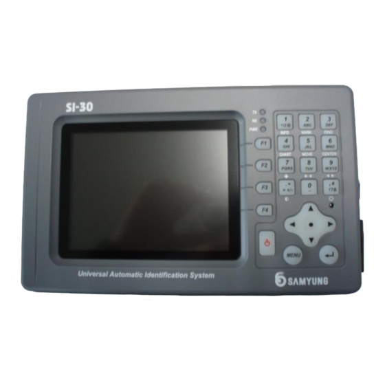
- Page 1 SERVICE MANUAL MODEL SI-30 Universal Automatic Identification Systrm...
- Page 2 1 Summary Description: 1-1 MMSI IMO and static information (NAME, CALL SIGN) How to set MENU [ TARGET LIST ] On the screen Press. MENU on the screen 2.INIT SETUP 2.SET STATIC DATA INIT SETUP screen Enter password Enter Administrator Password.
- Page 3 Store if you want Press the button and the information is stored. 1-2 GPS ANT How to set the position [ TARGET LIST ] On the screen MENU Button, then press the MENU screen high 2.INIT SETUP INIT SETUP screen. SET GNSS ANTENNA POSITION Enter the password --- * Enter the Administrator Password.
- Page 4 Store if you want Press the button and the information is stored. 1-3. Sense How to connect external GPS HEADING defense (EXTERNAL 422 INTERFACE) SEN terminal → external GPS input RXA15 (+) RXB14 (-) SEN terminal → HEADING input RXA18 (+) RXB17 (-) SEN1 SEN2 1-4.
- Page 5 Each Itemized Port The definition As follows: Like. 1 GPS: Inside GPS Transfer rate(Internal GPS Baud Rates) 2 SEN1: Sensor Port1 3 SEN2: Sensor Port2 4 SEN3 Sensor Port3 5 SEN4: Reserved 6 LONG: Long Range Port 7 AUX AUXILIARY Port 8 SPARE: Not Used 9 MKD: Transponder and MKD Between Transfer rate 10 GPS DIFF: DGPS Port...
- Page 6 Modification Upon completion SAVE button is pressed, the following screen will be displayed Save Wonhalttaeneun When you do not want to save the YES button, Press the NO button. 1-5. How to Change Your Password SYSTEM SETUP Mode Button By SET PASSWORDBy To move Next Button If you press Under Screen Emerges.
- Page 7 SAVE Press Button Pressing Under Screen Appears. Changes If you want YES Button,Any If Button Pressing Each Is performed *[ TARGET LIST ] On the screen =+/- BRIGHTNESS by pressing the button and adjust ---- The Night Mode button is pressed, the screen is switched to !?&...
- Page 8 CPA / TCPA: CPA (Closest Point to Approach)A Other Ships and Charity Approach Be Most Close Point Say, TCPAA CPAIn To reach Until Time Means. Target 10 knot O wn 5 knot Over In the figure, Charity(Own)And Other Marine(Target)This Each 5 knotWith 10 knotOf At a rate Movement Is Time Each On time According Two Spot Between Distance Available Number Have.Time t1,t2,t3,...,tnDay Time Each Between the points Distance Ask Time t3From Two Point Most Nearing the Egg Number Have.This...
- Page 9 Display Is. Then Next,In front of Figure and Like CPA Distance and Time Enter.Thus If you set User That has been set Time Within Charity and Other Of the vessel CPA Distance Specify who Than the distance Nears Alarm Occurs. 3 PROGRAM UPLOAD...
- Page 10 Program Upload a MKDA By Transponder Or Other MKD Program Upgrade to Is a function.Upload How Below Like. 3-1 TRANSPONDER UPLOAD TRANSPONDERIn UPLOADTo In order TRANSPONDERWith MKDA Normally Connection and Following The order Follow. DC 24V IN DC 24V IN TRANSPONDER TRANSPONDER Data cable...
- Page 11 [TRANSPONDER UPLOAD]A Selection Once Following Screens Sequentially Will be displayed Upload Progress is.Stage,Upload Among the Necessarily Transponder and MKDOf Power Turned off, or Connection Unbroken So that Note. Picture 2 Transponder EEPROM delete screen...
- Page 12 Picture 3 Transponder Application screen Picture 4 Transponder FPGA upload screen...
- Page 13 Picture 5 Transponder After uploading complete standby screen Upload After Under Screen Appears MKDA "Beep~" Sound Continue Ringing.At this time, MKDOf No Kina Press throw Restarts the When the Upload a Is completed. Picture 6 Transponder Upload is complete, the screen...
- Page 14 3 -2 MKD UPLOAD MKDWith MKDA By connecting Upload To In order Below Like Connected After Each MKDIn UPLOADWith DOWNLOAD Menu Execute. Connector Data cable DC 24V IN Picture 7 Connection with MKD MKD diagram Description For Upload To run the MKDA MKD-ASaid And,Download Subject MKDA MKD-BSaid Is.MKD-AIn Upload Menu Selection and MKD-BIn Download Menu Select the Two During the Which That First, even if On the behavior More than Not.Stage,Always Latest Version of the MKDThe Upload So Must Is.
- Page 15 Connector on the Connect When Upload/Download to Regardless of Both Which It anywhere MKDA Connect Is.Connector Power Connection DC 24VA Is used(Transponder Power AS When you use Is) 1) MKDOf Upload/Download Methods of Full Survey MKDWith MKD Between Upload/Download How Below Like. a.
- Page 16 2.2. MKD-A 3. MKD-B MENU MAINTENANCE] 3.1.1. Download PROGRAM UPLOAD] F3 8 F3 9 F3 7 Button At the same time Press. About 3Second After Download 3 5 3 5 3 5 3 5 3 5 3 5 Begins. UPLOAD] 2) MKD Upload Preparations MKD-AIn Upload Preparation For Below Like Is.
- Page 17 [MKD UPLOAD]A Selection and Once Under Screen Is displayed Upload Preparations State Is.Stage,Upload Not completed Until Never MKD Between Connection Off no matter Power Hotwire Should.
- Page 18 MKD-A Picture 9 MKD ready to upload screen MKD-A Picture 10 Associated with MKD to download and upload is in progress, the screen 3) MKD Download Preparations(New) MKD-BIn Download Preparation For Below Like Is. MENU In the initial screen, Button Press. Button or Use the buttons [4 MAINTENANCE] - -[7 PROGRAM...
- Page 19 [PROGRAM DOWNLOAD]A Selection Once Under Screen displayed,Download Begins.Stage,Download Not completed Until Never MKD Between Connection Off no matter Power Hotwire Should. MKD-B Picture 11 Download Ready screen...
- Page 20 MKD-B Picture 12 Download Screen to delete the ROM after MKD MKD-B Picture 13 Download Received in the ROM to record screen...
- Page 21 MKD-B Picture 14 Download Screen 1 has successfully completed MKD-B POWER OFF!! Picture 15 Download Screen 2 has successfully completed Download Upon completion Over Screen Appears "Beep~" Sound Continue Ringing.At this time, MKDA Restarts When Download completed.Stage,Download Not completed Until Never MKD Between Connection Off no matter Power Hotwire Should.
- Page 22 Sphericity MKDA PROGRAM DOWNLOAD Menu Does not exist Do.Therefore Sphericity MKDIn Download order initial screen, F3 7 F3 8 F3 9 Press and hold the button at the same time. About 3 seconds after the screen described above is displayed, the download process. More screen 2) MKD ready to download (new)See...
- Page 23 3 -3 MAP UPLOAD MAPHow to upload 1.2 MKD UPLOADSee Menu, select the As follows. MENU In the initial screen, Button Press. Button or By [4 MAINTENANCE] - -[8 PROGRAM UPLOAD] - 3 5 3 5 3 5 3 5 3 5 3 5 -[3 MAP UPLOAD] - Order Select.
- Page 24 3-4. How to check the version MENU After the upload is complete, in order to determine the version [4 MAINTENANCE] - - [1 PROGRAM VERSION] - Is selected. 056-019 Picture 16 Version confirmation screen From the bottom of the screen displays the version shown in V512-056- 019The actual version.
- Page 25 How to download from MDK PC 1 ComPort to run the program aisdownload set. (Pc of 1com - 4com). 2 Specifies the address of the download files. Down load address booter.bin -> bfc00000 map.bin -> bf000000 mkdmain.bin -> bfd00000 Select the file, and then select Send to. 3 MKD and then 5 +6 +7 F3-down mode until you press the When completed, the buzzer sounds.
- Page 26 4 Equipment photos 4-1 MKD front 4-2 MKD internal A-106...
- Page 27 4-3 MKD inside the back of the 4-4 MKD back of the...
- Page 28 4-5. TRANSPONDER top. 4-6. TRANSPONDER front...
- Page 29 4-7. TRANSPONDER internal V-889 CPU...
- Page 30 4-8. TRANSPONDER internal V-994 RF 4-9. SDBB-25P V-950 CONNECTION BOARD 4-10. IN / OUT V-638 CONNECTION BOARD...
- Page 32 5 The overall configuration BLOCK DAGRAM LCD(EDT : A056DN01) A-102 A-106 MAIN BOARD 320 X 234 DOT CONNECTOR BOARD MKD SIERAL POWER PWM POWER(-10V) RS-422 SDRAM FLASH MEMORY DC/DC CONVERTER DRIVER SERIAL IN/OUT PWM POWER(+15V) MKD SIERAL COUPLER ......PILOT SERIAL IN/OUT D/A COVERTER...
- Page 33 6 INT / EXT WIRING DIAGRAM SCHEMATIC MKD MECHANICAL(=SY) TRANSPONDER MECHANICAL(=SY) VHF ANT SAN-150 LCD-DATA-CONNECTOR V-884(RF-PCB) VGL(-10V) FMT:BNC-CLIP VGH(+15V) (OR, VB40-2071) STVR STVL CHASSIS POWER- T_ON/OFF POWER- SMB:R114426000 MKD_TXA VCOM MKD_TXB VCOM MKD_GND POWER+ HARTING:0918-564-7914 MKD_RXA POWER+ MKD_RXB STHL POWER+ MKD-TXB 64P-FLAT CABLE STHR...
- Page 34 7 SI-30D MKD electronic drawings 7-1 A-100 CPU BOARD LCD_D0 LCDO_D0 LCD_D1 LCDO_D1 LCD_D2 LCDO_D2 LCD_D3 LCDO_D3 LCD_FCLK LCDO_FCLK LCD_LCLK LCDO_LCLK LCD_ENAB LCDO_ENAB SDA12 D3 SDA12 LCD_PCLK LCDO_PCLK U0TXD(GP212) MKD_TX SDA11 D1 SDA11 DATA_1 DATA_3 FCLK PCLK +3.3V U0RXD MKD_RX SDA10 E5 SDA10 +3.3V...
- Page 35 7-2 A-100 POWER BOARD +12V +24V +12V CHASSIS FGND LED1 MKD_TXA MKD_TXA 0.1uF/630V MKD_TXB MKD_TXB LED2 MKD_GND GREEN 1 +VI MKD_RXA MKD_RXA MKD_RXB MKD_RXB 2 -VI POWER+ 2.2K 0.1uF 2.2K POWER+ KM-04 470/16 4 CNT POWER+ SPX-62S POWER- 0.1uF/630V PTS15-24-12 POWER- IF(AV)=6A LM2575...
- Page 36 7-3 A-101 KEY BOARD +3.3V +3.3V +3.3V SEL-0 * 22EA HST1122 SEL-0 SEL-1 SEL-1 POWER SW23 SEL-2 SEL-0 SEL-2 ON/OFF SEL-3 HST1122 SEL-3 SEL-4 SEL-4 RET-0 RET-4 RET-1 RET-3 RET-2 SEL-1 RET-2 RET-3 RET-1 RET-4 RET-0 SW10 SW11 SW12 SW10 ON/OFF SW11 SW12...
- Page 37 7-4 A-102 CONNECTOR BOARD HH-1M2012-301 CHASSIS SHIELD TP_RESET TP_RESET TP_RESET TP_RESET MKD_RXA PILOT_TXA MKD_RXA PILOT_TXA MKD_RXB PILOT_RXA MKD_RXB PILOT_RXA MKD_GND MKD_GND MKD_TXA MKD_TXB MKD_TXA MKD_TXB INTERNAL MKD_TXB MKD_RXA MKD_TXB MDK_RXA A-100 MKD CPU BOARD VALVE_STAUTS VALVE_STATUS VALVE_DOWN POWER+ POWER+ POWER+ CONNECTION POWER+ EXTERNAL...
- Page 38 7-5 MKD LINE BLOCK DIAGRAM 120mm FFC CABLE AWG #28 * 12EA DATA0 KFC : AWM 2896 80C VW-1 1 SHIELD DATA1 PITCH : 1.25mm , T : 0.3mm DATA2 3 PILOT_TXA CHASSIS DATA3 4 PILOT_RXA DISPOFF(DATA ENABLE) MKD_RXA FLM(FCLK) 6 MKD_TXB MKD_RXB MONO...
- Page 39 8 SI-30 TRANSPONDER 8-1 RF BOARD +12V TP44 32×2 STRT EJEC 0.1 SK1_9 SK1_10 SK1_11 SK1_12 LNA_ON TXE_3 TXE_2 TXE_1 RX2_BW_SEL RX1_BW_SEL +12V LD_SYNTH2 LD_SYNTH1 PAD1 SK1_23 REF_TUNE PWR_CNTRL PAD2 SK1_28 SK1_29 12V_MONITOR TX_REV TX_FWD RX3_RSSI RX2_RSSI RX1_RSSI EEPROM_S1 EEPROM_NCS...
- Page 40 8-2 RX FRONT END +12V LM2931 +9V LNA SUPPLY 8 IN 7 GND 6 GND 5 ON/OFF 10/16(T) R263 R185 R127 100K C279 R242 3 WAY SPLITTER 100R 100R 100n TP58 TP55 TP57 TP50 TP51 TP52 R245 R262 RX3_FE TR23 BC858B R340 82nH...
- Page 41 8-3 RX1 MIX +5V_RX1 TP68 R211 Mixer and IF R132 C208 C255 470nH -3dB 680R C316 100n MA04627 C394 R143 R270 R188 330R ADE-1HW 270nH 3 RF RX1_FE TP284 IF_RX1 C329 C330 C200 R363 R116 C175 TR26 100p 330R 330R BFR520 L107 R364...
- Page 42 8-4 RX2 MIX +5V_RX2 TP92 R216 R133 Mixer and IF C210 C260 470nH -3dB C321 680R 100n MA04627 C406 R145 R260 C342 R189 330R ADE-1HW 270nH 3 RF RX2_FE TP285 IF_RX2 C343 C202 R365 R120 C161 TR28 100p 330R 330R 220nH BFR520 R366...
- Page 43 8-5 RX3 MIX +5V_RX3 TP93 R218 330nH Mixer and IF C212 R134 C263 100n 820R MA04627 TP14 R129 R261 C344 L103 R190 ADE-1HW 470R 150nH C291 3 RF RX3_FE C229 TP286 IF_RX3 C345 C203 R367 R122 L102 TR30 270R 270R 150nH BFR520 R368...
- Page 44 8-6 RX1 IF / DEMOD IF AMP 1 +5V_RX1B +5V_RX1B TP128 TP22 R323 R119 C397 R111 C395 BLM41P800S C259 R307 10/16(T) 10/16 100n C322 470nH C214 R151 C159 BF998 R384 R350 3 G2 F16/A F16/B 820nH MA02065-45.1MHZ-G15B1 MA02065-45.1MHZ-G15B1 560nH 560nH 4 G1 TP274 IF_RX1...
- Page 45 8-7 RX2 IF / DEMOD +5V_RX2B IF AMP 2 R325 TP159 +5V_RX2B R121 TP27 TP10 R112 C410 C409 BLM41P800S C446 C447 10/16(T) 10/16(T) 100n R308 470nH C338 C162 C236 R370 BF998 R351 R389 3 G2 F20/A F20/B C209 FILTER-45.0MHZ-45G15B1 FILTER-45.0MHZ-45G15B1 820nH 4 G1 IF_RX2...
- Page 46 8-8 RX3 IF / DEMOD +5V_RX3B IF AMP 3 +5V_RX3B TP31 R328 TP184 TP33 C233 R123 BLM41P800S +3V3 C445 C223 10/16 10/16 R113 C231 R356 TP192 390nH R309 R355 C127 C348 TP191 C455 C123 R403 BF998 TP185 TP186 TP187 TP188 TP189 TP193 R391...
- Page 47 8-9 TX MODULATOR / SYSTH +5V_TX +5V_TX TP32 +6V_TX TP34 +5V_TX BLM41P8005 TP214 BLM41P8005 C254 C387 R289 100R TP207 C266 C265 22/16(T) 100n 22/16(T) 100n 100nH C389 R137 C256 100n 16dB C421 R252 ATTENUATOR C461 47nH TP208 820R C317 MA04627 TP281 100p 330R...
- Page 48 8-10 RX3 IF / DEMOD TP40 +12V 47nH TP225 47nH BAP64-03 RX_IN TP224 C106 R135 C107 PA DRIVER C105 TP220 BAP64-03 BAP64-03 TP222 TP223 IRFR9024 R324 TR43 BC858B BC858B R279 C101 R280 C102 TP218 TP219 TR44 TXE_2 BC846B R342 TP221 R341 TP226 TR20...
- Page 49 9 SI-30 BASEBAND BOARD 9-1 TOP-SHEET R204 3K3 PL5_1 LOCK_DISABLE R237 0R DSP_GPS_UARTTX GPS_UART0TX R238 0R GPS_UART_TX GPS_UART1TX R239 0R DSP_GPS_UARTRX GPS_UART0RX R240 0R (NF) (NF) (NF) (NF) (NF) (NF) (NF) (NF) GPS_UART_RX GPS_UART1RX SK1_14 GPIOA7 R107/A SK1_15 GPIOA6 R107/B...
- Page 50 9-2 DSP CORE PL1_1 PL1_3 1V26 PL1_5 Access to HOST port. HPIENA has internal pull-down resistor PL1_7 so it is default disabled. R37/A 33R PL1_9 R4/C 33R R37/B 33R 20×2 0.1 175 HD0/PGPI036 PL1_15 173 HD1/PGPI037 40 pin IDC header PL1_13 PL1_11 DVDD...
- Page 51 9-3 SDRAM SRAM AND FLASH SDRAM MEMORY FLASH MEMORY 64Mbit (×32) 2Mbit/4Mbit/8Mbit(x16) IC19 MT48LC2M32B2TG 1 VDD 15 VDD IC13 100n 10u/6.3 VDDQ 29 VDD SST39VF400 43 VDD 25 A0 17 A17 26 A1 48 A16 27 A2 1 A15 IO15 60 A3 2 A14 IO14...
- Page 52 9-4 CODECS AND SIGNAL CONDITIONING 10u/6.3 10u/6.3 100n 100n 10u/6.3 100n R114 100n 14 AVDD 100n CTLA_/CS 16 VMID SDIN CTL_DATA 15 AGND SCLK CTL_CLK 17 MICBIAS MODE 10u/6.3 DVDD BVDD C148 19 RLINEIN CODECA_RX1 DGND 18 MICIN R111/C 33R 20 LLINEIN CODECA_RX2 LRCIN...
- Page 53 9-5 FPGA C92 C93 C94 C95 C96 C111 C113 C112 C114 C115 C116 C10 C102 C104 C103 C108 C109 100n 100n 100n 100n 100n 100n 100n 100n 100n 100n 100n C110 IC21 100n 22u/6.3 10u/6.3 TPS76601C R146 Do not power multilinx 5 IN from this supply.
- Page 54 9-6 DAC AND ADC IC15/A LMV324 R174 C183 R175 R176 BUF_3V3 C184 IC15/B LMV324 C191 R186 100n 100n 10u/6.3 R177 C185 R179 R178 TLV5621I 1.2V 100n 2 REFA HWAT DAC_HWAT C186 3 REFB C235 DACA IC15/C 4 REFC 10u/6.3 DACB LMV324 5 REFD 10 +...
- Page 55 9-7 PORT INTERFACES 5VI7 5VI1 5VI4 5VI7 5VI1 5VI4 IC29 IC23 IC26 2 +VIN 2 +VIN 2 +VIN +VOUT +VOUT +VOUT C255 C253 1 GND C237 C196 C256 C246 C244 C259 1 GND 1 GND 100n 100n C236 100n 100n 100n 100n 100n...
- Page 56 9-8 POWER SUPPLIES FS2 1.5A 24V_IP POWER+ OUT+ PL16_1 C150 FUSE3A PL16_2 2200p240VAC C177 C211 MBRS2040LT3 SMCJ24A 330n 330n C146 C147 C210 C208 C209 330n 100/50 100/25(AL) 100/25(AL) 590uH 0V_IP POWER- OUT- C332 2200p240VAC R219 R201 220R R202 C220 IC22 L54 1uH LM2670S-ADJ C223...
- Page 57 9-9 V-900 POWER BOARD TP12 TP16 POWER+ OUT+ R273 R270 SFCB12604R0100 4.7K/0.25W 4.7K/0.25W EPC13 POWER+ C145 OUT+ 0.0022/100V 0.01/100V C194 LED10 BYW51G-200 C135 C149 EI-3329-A GREEN/3 0.001/100V 0.01/100V R269 C199 R268 30/1W SFPL-64 SFPL-64 0.001/100V 2.2K/1W R265 C207 C198 R274 470/50(NXB) R264 2.2K...
- Page 58 10 LED INDIGATOR BOARD LED1 304GC2E-003 LED2 12505-04A00 304YC2E-002 KRC101S KRC101S...
- Page 59 11 V-638 CONNECTION BOARD PL18_7 LONG_RNG_TX+ LONG_RNG_TXB LONG_RNG_TXB PL18_8 LONG_RNG_TX- LONG_RNG_TXA LONG_RNG_TXA PL18_9 GNDI2 LONG_RNG_GND LONG_RNG_GND PL18_11 LONG_RNG_RX+ LONG_RNG_RXB LONG_RNG_RXB PL18_12 LONG_RNG_RX(P.S) LONG_RNG_RXA LONG_RNG_RXA PL18_13 EXT_KEY_TX+ EXT_KEY_TXB EXT_KEY_TXB PL18_14 EXT_KEY_TX- EXT_KEY_TXA EXT_KEY_TXA PL18_15 GNDI4 EXT_KEY_GND EXT_KEY_GND PL18_17 EXT_KEY_RX+ EXT_KEY_RXB EXT_KEY_RXB PL18_18 EXT_KEY_RX(P.S) EXT_KEY_RXA...
- Page 60 12 A-107 GPS MODULE BOARD +3.3V CNH31R473S V_ANT V_BAT RESET_N +3.3V TXD1 RXD1 1000P TXD2 CNA30R223M HH-1M1608-121 RXD2 1000P 1 TXD2 GPS_RX2 TIMEPLUSE TIMEPULSE 2 RXD2 100P +3.3V GPS_TX2 EXTINT0 3 TXD1 GPS_RX1 USB-DP A3-20PA-2DSA 4 RXD1 GPS_TX1 USB-DM 5 VDDIO HH-1M1608-121 VDDUSB 6 VCC...
- Page 61 13 Power Supply SP-5ADC electronic drawings BRIDGE DIODE IRF540 KBPC350650A TRANS AC INPUT TRANS INPUT SW1-2 IRF540 CN12 OUTPUT POWER ON/OFF FMU-34S M0.1 15000/35 CN14 4.7K/2W SCN-20-3R CN13 FUSE DC24V INPUT SCN-20-2R SW1-1 FUSE M0.1 0.01/400 0.1/400 1N4007 4.7K 4.7K 0.01/400 PT1010 10/35...
Need help?
Do you have a question about the SI-30 and is the answer not in the manual?
Questions and answers
How to set cpa and tcpa?
To set CPA and TCPA on the Samyung SI-30:
1. Go to the CPA alarm settings.
2. CPA (Closest Point of Approach) is the minimum distance at which another ship will approach.
3. TCPA (Time to Closest Point of Approach) is the time until the closest approach happens.
4. Use the appropriate buttons to adjust CPA and TCPA values.
5. Set the desired distance for CPA and time for TCPA to trigger alarms when another vessel gets too close or will approach within a certain time.
These settings help monitor nearby vessels and prevent collisions.
This answer is automatically generated