Advertisement
Advertisement
Table of Contents

Subscribe to Our Youtube Channel
Related Manuals for Casio CTK-50


Summary of Contents for Casio CTK-50
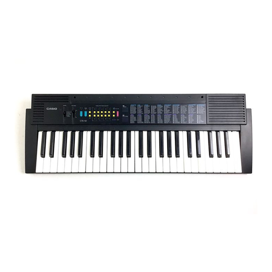
- Page 1 (without price) CTK-50 CTK-50 INDEX ELECTRIONIC KEYBOARD...
-
Page 2: Table Of Contents
SPECIFICATIONS GENERAL Number of keys: Polyphonic: 8-note Preset tones: Auto-rhythms: Auto-accompaniment: CASIO Chord/Fingered Demonstration tune: Classical Medley Built-in speakers: 10 cm dia. 2.0W Input Rating: 1 pc. Terminal: AC Adapter Jack (DC 9 V) Power source: 2-way AC or DC source... -
Page 3: Block Diagram
BLOCK DIAGRAM KO0~KO9 MSM6387-13 Amplifier Filter KI0~KI7 A4598 Q201 LSI201 Main Volume IC101 Speaker Keyboard VC +9 V AVDD +4.8 V VDD +5 V Power supply circuit Switches Q101, Q102, D102 Oscillator Q301, X301... -
Page 4: Circuit Description
Tone Rhythm (KC6) Tempo Tempo (KC7) Down Start/ Fill-In (KC8) Stop Demo (KC9) CASIO Normal Fingered Chord NOMENCLATURE OF KEYS F#3 G#3 A#3 C#4 D#4 F#4 G#4 A#4 C#5 D#5 F#5 G#5 A#5 C2 D2 G2 A2 C3 D3 G3 A3... - Page 5 CPU (LSI201: MSM6387-13) The CPU contains a sound data ROM and a DAC (Digital to Analog Convertor), and it provides a sound waveform in accordance with the pressed key and the selected tone. The following table shows the pin functions of LSI201. Pin No.
- Page 6 POWER AMPLIFIER (IC101: LA4598) The following table shows the pin functions of IC101. Pin No. Terminal In/Out Functiion Power GND Ground (0 V) source Ch1 B.S. Terminal for a bootstrap capacitor Ch1 OUT Channel1 output +9 V source. Connected to the power source directly. Ch1 N.F.
-
Page 7: Troubleshooting
POWER SUPPLY CIRCUIT The power supply circuit regulates two constant output voltages VDD (+5.0 V) for the CPU and the oscilla- tor, and AVDD (+4.8 V) for the analog circuit. VC (+9 V) Q101 D101 VDD (+5.5 V) R116 2SD1858Q,R Power Switch AVDD (+4.8 V) R101... -
Page 8: Major Waveforms
MAJOR WAVEFORMS 50 ns 2 ms – – CH1: 1V CH1: 5 V CH2: 5 V Clock pulse COSI Key scan signal KO0 MSM6387-13 pin 8 MSM6387-13 pin 30 Key scan signal KO1 MSM6387-13 pin 29 2 ms 2 ms CH1: 50 mV CH2: 50 mV CH1: 50 mV CH2: 0.5 V Sound signal output... -
Page 9: Schematic Diagrams
SCHEMATIC DIAGRAMS Keyboard PCB — 9 —... - Page 10 Main PCB Notes: µF). 1. All capacitance values are indicated in "µF" (p=10 Ω , M=10 Ω). 2. All resistance values are indicated in "Ω" (k=10 — 10 —...
-
Page 11: Pcb View
PCB VIEW Main PCB X301 No.2 FB101 C106 R116 JCM509-MA1M B JCM509-MA1M B R103 R209 NO.1 R301 R210 Q102 R303 R211 J101 R212 C222 No.2 L102 R213 C214 C217 R214 C108 R215 C218 R216 R108 C112 D202 C101 C109 R110 R112 D105 LSI201... -
Page 12: Exploded View
EXPLODED VIEW 17-1 17-2 17-1 17-1 17-4 13-1 13-2 17-3 — 12 —... -
Page 13: Parts List
PARTS LIST CTK-50 Notes: Prices and specifications are subject to change with- out prior notice. As for spare parts order and supply, refer to the "GUIDEBOOK for Spare parts Supply", published seperately. The numbers in item column correspond to the same... -
Page 14: Specifications
FOB Japan Item Code No. Parts Name Specification N.R.Yen Unit Price Electrical Parts 6923 2810 PCB ass'y JCM509-MA123M M240016*1 D101 2390 1316 Diode SB10-04A3-BT-T D102 2360 2044 Zener diode MTZJ6.2AT-77-T D103 2360 2429 Zener diode MTZJ4.3B-T77-T D104~D114, 2390 1344 Diode 1SS133T-77-T D201,D202 FB101... - Page 15 Description of Capacitors A general description of capacitors is shown in the following table. The description consists of Type, Value, Rated Voltage and Tolerance. When you need a capacitor, please find a subsutitution in your country by yourselves referring to the description.
- Page 16 8-11-10, Nishi-Shinjuku Shinjuku-ku, Tokyo 160, Japan Apr, 1995 Telephone: 03-3347-4926...
Need help?
Do you have a question about the CTK-50 and is the answer not in the manual?
Questions and answers