Chapters
Table of Contents

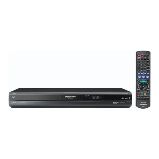
Related Manuals for Panasonic DMR-EX93CEG


Summary of Contents for Panasonic DMR-EX93CEG
- Page 1 ORDER No. DSD1006036CE DVD Recorder DMR-EX93CEG Model No. Vol. 1 Colours (S).......Silver Type (K).......Black Type © Panasonic Corporation 2010. Unauthorized copying and distribution is a violation of law.
-
Page 3: Table Of Contents
TABLE OF CONTENTS PAGE PAGE 1 Safety Precautions----------------------------------------------- 4 1.1. General guidelines ---------------------------------------- 4 2 Warning -------------------------------------------------------------- 5 2.1. Prevention of Electrostatic Discharge (ESD) to Electrostatic Sensitive (ES) Devices -------------- 5 2.2. Precaution of Laser Diode------------------------------- 6 2.3. Service caution based on legal restrictions --------- 7 3 Service Navigation ----------------------------------------------- 8 3.1. -
Page 4: Safety Precautions
1 Safety Precautions 1.1. General guidelines 1. When servicing, observe the original lead dress. If a short circuit is found, replace all parts which have been overheated or damaged by the short circuit. 2. After servicing, see to it that all the protective devices such as insulation barriers, insulation papers shields are properly installed. -
Page 5: Warning
2 Warning 2.1. Prevention of Electrostatic Discharge (ESD) to Electrostatic Sensitive (ES) Devices Some semiconductor (solid state) devices can be damaged easily by static electricity. Such components commonly are called Elec- trostatic Sensitive (ES) Devices. Examples of typical ES devices are integrated circuits and some field-effect transistor-sand semi- conductor "chip"... -
Page 6: Precaution Of Laser Diode
2.2. Precaution of Laser Diode... -
Page 7: Service Caution Based On Legal Restrictions
2.3. Service caution based on legal restrictions 2.3.1. General description about Lead Free Solder (PbF) The lead free solder has been used in the mounting process of all electrical components on the printed circuit boards used for this equipment in considering the globally environmental conservation. The normal solder is the alloy of tin (Sn) and lead (Pb). -
Page 8: Service Navigation
3 Service Navigation 3.1. Service Information 3.2. Caution for DivX... -
Page 9: Micro Fuse Conducting Check
3.3. Micro Fuse conducting check This unit uses the Micro Fuse. Check the Micro Fuse conducting using the Tester at the check points below. -
Page 10: Operation Check When A Usb Device Is Connected
3.4. Operation check when a USB device is connected You can check the operation status (normal or abnormal) of the USB connection part of this unit easily as shown below. Connect each device to the USB terminal on the front panel and check the operation status on the TV monitor. Normal operation: Automatically displayed when the USB connection is made to a digital camera, etc. -
Page 11: Specifications
4 Specifications... -
Page 14: Location Of Controls And Components
5 Location of Controls and Components... -
Page 16: Operating Instructions
6 Operating Instructions 6.1. Taking out the Disc from DVD-Drive Unit when the Disc cannot be ejected by OPEN/CLOSE button 6.1.1. Forcible Disc Eject 6.1.1.1. When the power can be turned off. 1. Turn off the power and press [STOP] [CH UP] keys on the front panel simultaneously for 15 seconds. 6.1.1.2. - Page 17 1. Turn off the power and pull out AC cord. 2. Remove the Top Case. 3. Put deck so that bottom can be seen. 4. Slide SLIDE CAM by Paper Clip or minus screw driver (small) in the direction of arrow to eject tray slightly. 5.
-
Page 18: Service Mode
7 Service Mode 7.1. Self-Diagnosis and Special Mode Setting 7.1.1. Self-Diagnosis Functions Self-Diagnosis Function provides information for errors to service personnel by “Self-Diagnosis Display” when any error has occurred. U**, H** and F** are stored in memory and held. You can check latest error code by transmitting [0] [1] of Remote Controller in Service Mode. Automatic Display on FL will be cancelled when the power is turned off or AC input is turned off during self-diagnosis display is ON. - Page 19 Error Code Diagnosis contents Description Monitor Display Automatic FL display ST Microprocessor Display appears when ST Microprocessor No display Communication Error Communication Error on Timer Bus occurs. Timer U80 is displayed till the [POWER] key is pressed. ST Microprocessor Display appears when ST Microprocessor No display Communication Error...
- Page 20 Error Code Diagnosis contents Description Monitor Display Automatic FL display HARD Drive error The drive detected a hard error. “DVD drive error.” Display for 5 seconds. The character indication flows side- ways. SELF Restoration operation Since the power cord fell out during a power No display CHECK failure or operation, it is under restoration...
- Page 21 Item FL display Key operation Mode name Description Front Key Service Mode Setting every kind of modes for servicing. When the power is off, press [CH *Details are described in “7.1.3. Service UP], [OPEN/CLOSE] and [REC] Modes at a glance”. keys simultaneously for 5 seconds.
- Page 22 Item FL display Key operation Mode name Description Front Key Aging Contents (Example): Demonstration lock/ Ejection of the disc is prohibited. *When lock the tray. When the power is on, press unlock The lock setting is effective until unlocking the [STOP] and [POWER] keys simulta- tray and not released by “Main unit initializa- neously for 5 seconds in the condi-...
- Page 23 Item FL display Key operation Mode name Description (Remote controller key) Release Items Item of Service Mode executing is cancelled. Press [0] [0] in service mode. Error Code Display Last Error Code of U/H/F held by Timer is dis- Press [0] [1] in service mode played on FL.
- Page 24 Item FL display Key operation Mode name Description (Remote controller key) RTSC Return in XP AV1 input signal is encoded (XP), decoded Initial mode: EE2/ Interlace/ XP/ Audio Press [1] [3] in service mode. (A & V) (XP) and output decoded signal to external 48kHz without DISC recording and DISC playback.
- Page 25 Item FL display Key operation Mode name Description (Remote controller key) READ SEEK Inspecting seek time of HDD to inspect per- At start Press [3] [1] in service mode. Inspection formance. * When canceling the inspection mode while executing, do “forced power-off”.
- Page 26 Item FL display Key operation Mode name Description (Remote controller key) HDD READ VERIFY Measure of access time in READ VERIFY At start Press [3] [2] in service mode. Inspection MODE of HDD. * When canceling the inspection mode while executing, do “forced power-off”.
- Page 27 Item FL display Key operation Mode name Description (Remote controller key) HDD Simple AV Scan Simple AV scan check of HDD Press [3] [6] in service mode. * When canceling the inspection mode while executing, do “forced power-off”. Method: Press [POWER] key on the main unit more than 4 seconds.
- Page 28 Item FL display Key operation Mode name Description (Remote controller key) HDD/ DVD Drive Sim- Check if HDD Self-Diagnosis test was per- HDD Self-Diagnosis test start. Press [3] [8] in service mode. ple Check formed or Drive last error occurred within 4 weeks.
- Page 29 Item FL display Key operation Mode name Description (Remote controller key) DVD Drive Last Error DVD Drive error code display. 1. Error Number is displayed for 5 sec- Press [4] [2] in service mode. *For details about the drive error code, refer onds.
- Page 30 Item FL display Key operation Mode name Description (Remote controller key) Turn on all FL/LEDs All segments of FL and all LEDs are turned All segments are turned on. Press [5] [1] in service mode. PB HIGH Signal Out- 8 pin of AV 1 Jack (PB HIGH terminal) is High Press [5] [2] in service mode.
- Page 31 Item FL display Key operation Mode name Description (Remote controller key) Display the Error His- Display the Error History stored on the unit. Display reason of error for 5 seconds. Press [6] [5] in service mode. tory Then press [0] [1] ~ [9] [9], the past 99 error histories are displayed.
- Page 32 When USB check is OK. * Insert USB memory. [*] is volume label. Example of volume label is [PANASONIC] : When USB check is NG. AV4(V)/AV1(RGB) I/O Set input to AV4 (V) and set output to AV1 Press [8] [0] in service mode.
- Page 33 Item FL display Key operation Mode name Description (Remote controller key) Error code initialization Initialization of the last error code held by Press [9] [8] in service mode. timer (Write in F00) Initialize Service Last Drive Error, Error history and Error Press [9] [9] in service mode.
-
Page 34: Service Fixture & Tools
8 Service Fixture & Tools Part Number Description Compatibility RFKZ0260 Extension Cable (Main P.C.B. - Digital P.C.B./ 88 Pin) Same as EH49 Series RFKZ0323 Extension Cable (Main P.C.B. - Power P.C.B./ 9 Pin) Same as EH49 Series RFKZ0455 Extension Cable (HDD - Digital P.C.B./ 7 Pin) Same as EX795 Series RFKZ0169 Extension Cable (Main P.C.B. -
Page 35: Disassembly And Assembly Instructions
9 Disassembly and Assembly Instructions Note: In this document, explanations basically use illustrations of DMR-EH63/635. For DMR-EH53/535, shape of some parts may be different. 9.1. Disassembly Flow Chart The following chart is the procedure for disassembling the casing and inside parts for internal inspection when carrying out the ser- vicing. -
Page 36: P.c.b. Positions
9.2. P.C.B. Positions... -
Page 37: Top Case
9.3. Top Case 9.4.1. How to assemble Tray door 1. Attach the Tray door spring to Tray door. 1. Remove 2 screws (A) and 3 screws (B). Slide Top Case rearward and open the both ends at rear side of the Top Case a little and lift the Top Case in the direction of the arrows. -
Page 38: Front (L) P.c.b., Front (R) P.c.b
9.5. Front (L) P.C.B., Front (R) 1. Remove 4 Screws (A), SATA Power Cable and SATA Sig- nal Cable to remove HDD. P.C.B. 1. Remove 2 Screws (A) to remove the Front (L) P.C.B. and Front (R) P.C.B. 9.6. 2. Put HDD with HDD bracket up and down inversely so as not to give a shock to HDD. -
Page 39: Dvb-C Ci P.c.b
9.7. DVB-C CI P.C.B. 3. Remove 2 Screws (C) from DVB-S Bracket Rear, CI Bar- rier, and DVB-S Bracket Rear. 1. Remove 2 Screws (A), FFC, and Power Cable. 2. Remove 2 Screws (B) from Rear Panel and DVB-C CI 9.8. -
Page 40: Ram/Digital P.c.b. Module
9.8.2. Rear Panel with Fan Motor 2. Lift up Digital P.C.B. slightly so to disconnect the Connec- tor to remove Digital P.C.B. in the direction of the arrow. 1. Remove 5 Screws (B) and 2 Screws (C). And remove 3 Screws (B) to remove DVD drive. 2. -
Page 41: Power P.c.b
Note: 9.10. Power P.C.B. RAM/Digital P.C.B. Module as service part has no Heat 1. Remove 2 Screws (A) and disconnect the Connector to transfer sheet. remove Power P.C.B. Before returning to customer, Heat transfer sheet and Sheet cover should be installed on Digital P.C.B. -
Page 42: Main P.c.b
9.11. Main P.C.B. 1. Remove 5 Screws (A) and disconnect the Connector. 2. Remove Front angle and 2 Digital PCB bracket. 3. Remove Main P.C.B. 4. Remove P.C.B. Spacer from Main P.C.B. Pull out DVB-C CI P.C.B. from the P.C.B. Spacer with holding the spreading part. -
Page 43: Measurements And Adjustments
10 Measurements and Adjustments 10.1. Service Positions Note: For description of the disassembling procedure, see the section 9. 10.1.1. Checking and Repairing of DVB-C CI P.C.B. - Page 44 10.1.2. Checking and Repairing of Power P.C.B.
- Page 45 10.1.3. Checking and Repairing of RAM / Digital P.C.B. Module...
- Page 46 10.1.4. Checking and Repairing of Main P.C.B.
- Page 47 10.1.5. Checking and Repairing of HDD...
-
Page 48: Caution For Replacing Parts
10.2. Caution for Replacing Parts 10.2.1. Items that should be done after replacing parts *Note1:... - Page 49 *Note2: Please prepare latest firmware updating disc. * Main Firm is being recorded in HDD, but new HDD has no data. Writing Procedure of Main Firm: <<Caution>> (1) Writing of Main Firm needs 3, 4 minutes. (2) Never cut the power of DVD Recorder until writing in Firmware ends. (3) Initial settings and contents of reservation will not change if writing is normally completed.
-
Page 50: Standard Inspection Specifications After Making Repairs
Perform auto recording and playback for one minute using the RAM No abnormality should be seen in the picture, sound or operation. disc. *Panasonic DVD-RAM disc should be used when recording and playback. Model with the HDD: Perform auto recording and playback for one No abnormality should be seen in the picture, sound or operation. - Page 51 "Standard-Playback" mode when there is no specify mode is mentioned. Model No. DMR-EX93CEG 4.Although the voltage and waveform available on here is measured with standard frame, it may be differ from actual measurement due to modification of circuit and so on.
-
Page 52: S2. Voltage And Waveform Chart
S2. Voltage and Waveform Chart Note) Indicated voltage values are the standard values for the unit measured by the DC electronic circuit tester (high-impedance) with the chassis taken as standard. Therefore, there may exist some errors in the voltage values, depending on the internal impedance of the DC circuit tester. S2.1. -
Page 53: S2.2. Front_R P.c.b
S2.2. Front_R P.C.B. <P7402> REF NO. PIN NO. REC REF NO. PIN NO. REC REF NO. PIN NO. REC REF NO. PIN NO. REC P7402 P7402 Q1602 IC7701 P7402 P7402 Q1602 IC7701 P7402 P7402 Q1602 IC7701 P7402 P7402 Q1602 P7402 P7402 Q1602 P7402... -
Page 54: S2.3. Power P.c.b
S2.3. Power P.C.B. <T1150> REF NO. PIN NO. REC IC1150 IC1150 IC1150 IC1150 IC1150 IC1150 IC1150 IC1150 IC1150 IC1201 IC1201 IC1201 IC1201 Q1160 Q1160 Q1160 Q1200 Q1200 Q1200 Q1200 Q1220 Q1220 Q1220 Q1220 QR1220 QR1220 QR1220 T1150 T1150 T1150 T1150 T1150 T1150 T1150... -
Page 55: S3. Block Diagram
DR P ON P7402 P59001 ANALOG TIMER BLOCK SECTION QR1501 :ON) IC1201 (ERROR VOLTAGE DET.) Q1220 (FEED BACK) QR1220 P SAVE L P1102 P1501 P7402 P59001 FROM DIGITAL P.C.B. TIMER BLOCK SECTION COLD DMR-EX93CEG Main P.C.B. Power Supply Block Diagram (1/2) -
Page 56: S3.1.2. Main P.c.b. Power Supply Block Diagram (2
IP7802 IC7301- VOUT X SW+12.5V H :ON P7801 P91001 TO DVB-C CI P.C.B. 17.18 P59001 P7402 D+3.3V FROM DIGITAL P.C.B. DR+12V P7402 P59001 44,46 TO DIGITAL P.C.B. X SW+12V P7402 P59001 58,60,62,64 DMR-EX93CEG Main P.C.B. Power Supply Block Diagram (2/2) -
Page 57: S3.2. Main P.c.b. Analog Video Block Diagram
V SYNC OUT 82 AV2 G GREEN P7402 P59001 C SYNC OUT 86 (DECODER/EXT) AV2 B AV2 G BLUE CLAMP TU7801 AV2 V/Y VIDEO/Y (U/V TUNER) AV2 B TUNER CLAMP VIDEO CLAMP AV2 V/Y CLAMP DMR-EX93CEG Main P.C.B. Analog Video Block Diagram... -
Page 58: S3.3. Main P.c.b. Analog Audio Block Diagram
PS +11.6V POWER SUPPLY VCC 11R6V Q4001- C BLOCK (2/2) SECTION I/O P SAVE SERIAL IC3003- 3 CTL3 JK4901 OPTICAL (DIGITAL AUDIO OUT) FROM P59001 P7402 IEC OUT DIGITAL P.C.B. BACK END SECTION DMR-EX93CEG Main P.C.B. Analog Audio Block Diagram... -
Page 59: S3.4. Digital P.c.b. Analog Timer Block Diagram
P91001 P7801 P7402 P59001 TO MAIN P.C.B. DIG CS POWER SUPPLY BLOCK (2/2) SECTION ANT PON H P59001 P7402 ANT PON G UARTP2M A 32 RXD IC50001- DMR-EX93CEG DIGITAL P.C.B. G UARTM2P A Digital P.C.B. Analog Timer Block Diagram IC50001-... -
Page 60: S4. Schematic Diagram
RGB_CPSVIN RGB_CPSVIN CARTRIGE CARTRIGE IF OUT[-] IF OUT[-] DGND DGND REC INH REC INH DGND DGND V_YIN_DM V_YIN_DM CLOSE SW CLOSE SW R_IN R_IN DGND DGND B_IN B_IN CPNCIN_DM CPNCIN_DM G_IN G_IN DMR-EX93CEG DVB-C CI .PC.B. Interconnection Schematic Diagram S-10... - Page 61 S-11...
-
Page 62: S4.2. M_Net_Fl (M) Schematic Diagram
S4.2. M_NET_FL (M) Schematic Diagram DMR-EX93CEG M_NET_FL Section (Main P.C.B. (1/3)) Schematic Diagram (M) Modify Category VariationCategory Variation Type C/D/E/F EH535EG C7405 $[F2A1A181A397] $[F2A1A181A397] $[F2A1A181A397] $[F2A1A181A397] $[F2A1A181A397] $[F2A1A181A397] EH53EC C7501 F2A0J471A832 F4D55473A013 F4D55473A013 F4D55473A013 F4D55473A013 F4D55473A013 EH53EP,EE J0JBC0000134 J0JBC0000134 EH635EG... - Page 63 DMR-EX93CEG M_NET_FL Section (Main P.C.B. (1/3)) Schematic Diagram (M) DP7501 A2BD00000192 Q7502 K7505 B1ADLB000006 VWJ0795=20 D7510 B0ACCE000003 D7504 B0BA02100001 CL7523 [34]GR9 [23]SG10 QR7501 CL7524 B1GBCFLL0043 T7501 G4D1A0000117 IC7501 D7505 R7501 HOLTEK C0HBB0000061 B0AADM000003 5600 VEE_21V [43]VDD [44]VSS D7506 Q7501 B0AADM000003...
- Page 64 5600 F1H1C105A095 C1611 R1602 F2A1A4700041 ERJ3GEY0R00V Q1602 B1CFRD000023 [CPH6412] QR1601 B1GBCFNN0041 CL1506 L1505 Q1501 $[G0C100K00043] B1CHQD000010 VOUT [UPA1914-TE] K1604 ON[H] SENSE VWJ0795=5 IC1506 C0DAEYH00002 F1H1A105A028 C1526 R1505 QR1503 B1GBCFNN0041 DR_GND DMR-EX93CEG M_NET_FL Section (Main P.C.B. (1/3)) Schematic Diagram (M) S-14...
- Page 65 V_YIN_DM R_IN G_R_C_IN_A DGND B_IN G_B_IN_A G_CIN_DM_A CPNCIN_DM G_IN G_G_IN_A 05A028 CL7402 2010/12/31 DR_GND ZB7503 RMN0917 ZB7502 RMN0916 ZB7501 RMN0915 CL1502 CL1501 ZS1501 $[VFV0163] ZS1502 VFV0164 ZS1503 VFV0167 ZS1504 VFV0187 DMR-EX93CEG M_NET_FL Section (Main P.C.B. (1/3)) Schematic Diagram (M) S-15...
-
Page 66: S4.3. Av_Io (Av) Schematic Diagram
S4.3. AV_IO (AV) Schematic Diagram DMR-EX93CEG AV_IO Section (Main P.C.B. (2/3)) Schematic Diagram (AV) VariationCategory VariationCategory1 A/B/C D/E/F J/K/L A/B/C D/E/F J/K/L F1H1C104A071 F1H1C104A071 F1H1A105A028 F1H1A105A028 F1H1A105A028 C4004 C3005 │F1H1C104A001 │F1H1C104A001 │F1H1A105A036 │F1H1A105A036 │F1H1A105A036 │F1H1C104A041 │F1H1C104A041 F1H1A105A028 F1H1A105A028 F1H1A105A028 C4005... - Page 67 DMR-EX93CEG AV_IO Section (Main P.C.B. (2/3)) Schematic Diagram (AV) D3901 R3919 ACK000004 ERDS2TJ331T AV2_8 AV2_BLANKING G_AV2_VIN_A ZJ3002 K9ZZ00001279 JK3901 ZJ3001 K1FB242B0011 K9ZZ00001279 R3908 G_R_C_IN_A G_G_IN_A G_B_IN_A C3904 F1H1H101A004 R3926 C3903 F1H1H101A004 R3928 10K R3929 10K G_DT_IN_L_A G_TU_L_A R4002 G_DT_IN_R_A G_TU_R_A...
- Page 68 X_SW_12R5V Q4001 B1ADLB000006 K4002 G_IEC_OUT_A R4008 $[ERJ3GEY0R00V] VariationCategory2 3300 F1H1A105A028 A/B/C D/E/F R3001 ERJ3GEY0R00V ERJ3GEY0R00V C4905 R3008 R3014 R4001 C4904 QR4001 $[F2A0J470A599] B1GBCFJJ0040 R4002 R4003 R4004 R4014 R4015 R4018 R4019 DMR-EX93CEG AV_IO Section (Main P.C.B. (2/3)) Schematic Diagram (AV) S-18...
- Page 69 Type R3001 ERJ3GEY0R00V ERJ3GEY0R00V ERJ3GEYJ562V ERJ3GEYJ562V ERJ3GEY0R00V EH535EG R3008 2010.12.31 Until EH53EC R3014 EH53EP,EE R4001 EH635EG R4002 EH63EC R4003 EH63EP,EE R4004 EX773EB,EC,EP R4014 EX83EB R4015 EX83EC,EP R4018 EX83EG R4019 EX93CEG DMR-EX93CEG AV_IO Section (Main P.C.B. (2/3)) Schematic Diagram (AV) S-19...
-
Page 70: S4.4. Tuner (Tu) Schematic Diagram
S4.4. Tuner (TU) Schematic Diagram DMR-EX93CEG Tuner Section (Main P.C.B. (3/3)) Schematic Diagram (TU) Modify Category Variation Type EH535EG EH53EC EH53EP,EE EH635EG EH63EC EH63EP,EE EX773EB,EC,EP EX83EB EX83EC,EP EX83EG EX93CEG VariationCategory F1H1H472A013 F1H1H472A013 F1H1H472A013 F1H1H472A013 F1H1H472A013 F1H1H472A013 C7304 │F1H1H472A219 │F1H1H472A219 │F1H1H472A219 │F1H1H472A219... - Page 71 DMR-EX93CEG Tuner Section (Main P.C.B. (3/3)) Schematic Diagram (TU) IC7801 L7801 D7802 C7817 C7818 C7819 D7803 $[MAZ4051NMF] R7811 R7814 R7812 R7815 Q7802 R7816 Q7803 C7826 TU7801 C7822 C7820 F1H1H222A013 LB7801 K7801 J0JGC0000063 ACTIV_5V C7802 C7801 C7821 F1H1H103A219 ANT_5V R7802 D7801...
- Page 72 TU7802 ENGF7601GF ENGF7601GF ENGF7602GF │J0JGC0000020 │J0JGC0000020 │J0JGC0000020 │J0JGC0000020 │J0JGC0000020 │J0JGC0000020 J0JBC0000134 J0JBC0000134 J0JBC0000134 J0JBC0000134 J0JBC0000134 J0JBC0000134 LB7804 X7301 H0H184500008 H0H184500008 H0H184500008 H0H184500008 H0H184500008 H0H184500008 │J0JBC0000011 │J0JBC0000011 │J0JBC0000011 │J0JBC0000011 │J0JBC0000011 │J0JBC0000011 DMR-EX93CEG Tuner Section (Main P.C.B. (3/3)) Schematic Diagram (TU) S-22...
- Page 73 │J0JBC0000011 Cout AFT_OUT K1MN20A00013 VOUT K1KA05AA0180 VIDEO_OUT B1ABDF000026 │DSC500100L B1ABDF000026 │DSC500100L C7833 C7834 C7831 K7814 F1H1A105A028 F1H1A105A028 VWJ0795=10 C7830 IP7802 CL7802 2200 ECJ1VB1H103K Confidential 2010/12/31 1.5M Until 330K ENGF7714KF H0H184500008 DMR-EX93CEG Tuner Section (Main P.C.B. (3/3)) Schematic Diagram (TU) S-23...
-
Page 74: S4.5. Front_L Schematic Diagram
C7701 EVQ11A05R K1KA03AA0301 F1H1A105A028 C7702 CK7001 POWER $[F2A0J470A824] CK7002 NC OPEN CL7702 KEY_POWER CK7003 NC OPEN KEY OPEN CLOSE XSW5V CL7701 R7701 ERDS2TJ470T K1KA06B00150 PP7701 Confidential Confidential [PP] Until 2008/12/31 Until DMR-EX93CEG DMR-EX93CEG Front_L Front_R Schematic Diagram Schematic Diagram S-24... - Page 75 S-25...
-
Page 76: S4.7. Power Schematic Diagram
S4.7. Power Schematic Diagram DMR-EX93CEG Power Schematic Diagram CAUTION: FOR CONTINUED PROTECTION AGAINST FIRE HAZARD, REPLACE ONLY WITH THE SAME TYPE 2A 250V FUSE. ATTENTION: POUR UNE PROTECTION CONTINUE LES RISQUES 2A 250V D' INCENDIE N' UTILISERQUE DES FUSIBLE DE MÉME TYPE 2A 250V. - Page 77 DMR-EX93CEG Power Schematic Diagram COLD D1270 RADIATION D1270 ZA1271 XYN3+J8FJ B0JBSG000053 T1150 [FCHS10A065] R1123 ZA1270 G4DYA0000191 $[ERG2SJ473E] VSC5614-A [2W 47K] SAF_D_DCV_BT Ns12 Ns12 Ns12 P1102 K1KB09A00047 P_SAVE_L L1270 G0A100H00025 X_SW12V X_SW12V X_SW12V SAF_D_SNB X_SW12V LB1124 C1124 D1142 ERJ6GEY0R00V F1B2G1020002 $[B0HADV000001]...
- Page 78 [2KV 390P] D1157 R1152 R1151 B0HADV000001 [AP01CV2] R1158 C1154 D1152 ERX2SJR22E D1156 F1H1H471A792 B0BC01000014 [2W R22] B0ACCK000005 R1154 11K[D] D1161 B0ACCK000005 ZA1105 K9ZZ00001279 ZA1106 K9ZZ00001279 ZA1151 XYN3+J8FJ ZA1271 XYN3+J8FJ ZB1101 VariationCategory DMR-EH535EG DMR-EX93CEG ZB1101 VJF0309 DMR-EX93CEG Power Schematic Diagram S-28...
- Page 79 Q1200 B3PBA0000454 R1208 2200 C1200 R1210 F1H1C104A071 R1151 R1205 R1206 $(220K) 4700[D] D1152 B0BC01000014 R1154 11K[D] Q1220 B3PBA0000454 R1221 5600 QR1220 B1GBCFNN0041 Confidential 2011.12.31 Until VariationCategory DMR-EH535EG DMR-EX93CEG ZB1101 VJF0309 DMR-EX93CEG Power Schematic Diagram S-29...
-
Page 80: S5. Print Circuit Board
S5. Print Circuit Board S5.1. Main P.C.B. DMR-EX93CEG Main P.C.B. (Component Side) R7802 ZJ3001 W292 ZJ7407 ZJ7405 W169 TU7801 TU7802 W291 W106 C7819 X7301 C7312 P7802 W174 D7803 W278 W178 C7326 C7313 K4001 K4003 D7802 L7301 W243 K7814 P7801 K7301... - Page 81 DMR-EX93CEG Main P.C.B. (Foil Side) R3019 LB7801 R7306 C7806 R7310 LB7306 C7812 C7804 R7308 R7803 C7847 C7802 LB7804 R7804 LB7304 LB7803 C7807 W527 C7805 K7802 C7325 R3017 C7813 C7825 C7330 R7311 C7338 LB7805 C7827 C7818 C7820 K7804 C3037 C7810 R7812...
- Page 82 W260 K1501 LB1501 W142 C1549 W144 W127 C7501 W128 IC1506 W130 W129 W290 W203 W204 P7402 C1611 W183 W186 W188 L7401 W187 W301 W298 L4901 W299 C1545 K1604 L1505 W248 P1501 W249 (Component Side) DMR-EX93CEG Main P.C.B. (Component Side) S-32...
- Page 83 CL7414 C7410 C1613 CL7413 C7415 C1612 C1601 IBT63 C7403 C1614 CL1506 C7417 R7412 CL1504 C1602 C1605 C1610 CL7409 R7411 C1617 CL7406 G1502 TL7401 IC7404 CL7405 CL7404 CL7402 C1528 R1506 R1519 CL1505 C4905 (Foil Side) DMR-EX93CEG Main P.C.B. (Foil Side) S-33...
-
Page 84: S5.2. Front_L P.c.b
S5.2. Front_L P.C.B. / S5.3. Front_R P.C.B. IC7701 S7201 S7701 R7701 C7702 PP7701 P7201 (Component Side) (Component Side) CL7702 C7701 CK7001 CK7003 CL7701 CK7002 (Foil Side) (Foil Side) DMR-EX93CEG DMR-EX93CEG Front_L P.C.B. Front_R P.C.B. S-34... - Page 85 S-35...
-
Page 86: S5.4. Power P.c.b
S5.4. Power P.C.B. DMR-EH535EG Power P.C.B. (Component Side) ZA1105 L1120 R1101 VA1110 C1121 C1126 C1122 L1121 C1143 S-36 S-36 R1123 R1122... - Page 87 DMR-EH535EG Power P.C.B. (Foil Side) LG1111 LG1114 LG1112 LG1104 LG1107 LG1105 LB1126 S-37 S-37 D1160 R1156...
- Page 88 C1122 L1121 C1143 R1123 R1122 D1158 R1159 D1142 D1157 C1150 T1150 ZA1270 C1270 C1271 D1270 C1272 IC1200 P1102 ZA1106 L1270 (Component Side) DMR-EH535EG Power P.C.B. (Component Side) S-38...
- Page 89 LB1126 D1160 R1156 R1152 Q1160 C1152 R1160 R1151 R1154 D1161 D1155 R1153 R1150 R1161 QR1220 R1209 R1221 C1200 R1201 R1208 R1200 R1207 C1201 (Foil Side) DMR-EH535EG Power P.C.B. (Foil Side) S-39...
- Page 90 S-40...
-
Page 91: S6. Abbreviation
S6. Abbreviation INITIAL/LOGO ABBREVIATIONS A0~UP ADDRESS ACLK AUDIO CLOCK AD0~UP ADDRESS BUS ADATA AUDIO PES PACKET DATA ADDRESS LATCH ENABLE AMUTE AUDIO MUTE AREQ AUDIO PES PACKET REQUEST AUDIO RF SERVO AMP INVERTED INPUT SERVO AMP OUTPUT ASYNC AUDIO WORD DISTINCTION SYNC BIT CLOCK (PCM) BCKIN BIT CLOCK INPUT... - Page 92 INITIAL/LOGO ABBREVIATIONS DREQ DATA REQUEST DRESP DATA RESPONSE DIGITAL SERVO CONTROLLER DSLF DATA SLICE LOOP FILTER DIGITAL VIDEO DISC ERROR TORQUE CONTROL ERROR TORQUE CONTROL REFERENCE ENCSEL ENCODER SELECT ETMCLK EXTERNAL M CLOCK (81MHz/40.5MHz) ETSCLK EXTERNAL S CLOCK (54MHz) FBAL FOCUS BALANCE FCLK FRAME CLOCK...
- Page 93 INITIAL/LOGO ABBREVIATIONS PWMCTL PWM OUTPUT CONTROL PWMDA PULSE WAVE MOTOR DRIVE A PWMOA, B PULSE WAVE MOTOR OUT A, B READ ENABLE RFENV RF ENVELOPE RF PHASE DIFFERENCE OUTPUT (CD-ROM) REGISTER SELECT RSEL RF POLARITY SELECT RESET RESERVE SBI0, 1 SERIAL DATA INPUT SBO0 SERIAL DATA OUTPUT...
- Page 94 INITIAL/LOGO ABBREVIATIONS TPSO OP AMP OUTPUT TPSP OP AMP INVERTED INPUT TRCRS TRACK CROSS SIGNAL TRON TRACKING ON TRSON TRAVERSE SERVO ON VBLANK V BLANKING COLLECTOR POWER SUPPLY VOLTAGE VCDCONT VIDEO CD CONTROL (TRACKING BALANCE) DRAIN POWER SUPPLY VOLTAGE VIDEO FEED BACK VREF VOLTAGE REFERENCE SOURCE POWER SUPPLY VOLTAGE...
-
Page 95: S7. Replacement Parts List
S7. Replacement Parts List Note: 1.* Be sure to make your orders of replacement parts according to this list. 2. IMPORTANT SAFETY NOTICE Components identified with the mark have the special characteristics for safety. When replacing any of these components, use only the same type. 3. - Page 96 DMR-EX93CEGK/S vol.1 Ref.No. Part No. Part Name & Description Remarks Ref.No. Part No. Part Name & Description Remarks C3908 F1H1H470A004 50V 47P RFKB79251LT MAIN P.C.B. 1 (RTL) E.S.D. C3909 F1H1H471A792 50V 470P VEP70334A FRONT (L) P.C.B. 1 (RTL) E.S.D. C3910 F1H1H470A004 50V 47P VEP70335A FRONT (R) P.C.B.
- Page 97 DMR-EX93CEGK/S vol.1 Ref.No. Part No. Part Name & Description Remarks Ref.No. Part No. Part Name & Description Remarks C7509 F1H1H104A748 50V 0.1U L1603 G0C100K00043 COIL 10UH C7512 F1H1C104A071 16V 0.1U L7301 G0C2R2JA0019 COIL 2.2UH C7565 F2A1C2210095 16V 220U L7401 G0C100JA0019 COIL 10UH C7569 F1H1H392A013 50V 3900 L7403...
- Page 98 DMR-EX93CEGK/S vol.1 Ref.No. Part No. Part Name & Description Remarks Ref.No. Part No. Part Name & Description Remarks R1609 ERJ3GEYJ474V 1/10W 470K R7312 F1H1H103A219 50V 0.01U R1610 D1BDR027A101 2W 0.027U R7401 ERJ3GEY0R00V 1/10W 0 R1611 ERJ3GEYJ363V 1/10W 36K R7402 ERJ3GEY0R00V 1/10W 0 R1612 ERJ3GEYJ474V 1/10W 470K R7405...
- Page 99 DMR-EX93CEGK/S vol.1 Ref.No. Part No. Part Name & Description Remarks Ref.No. Part No. Part Name & Description Remarks ZB7501 RMN0915 FL HOLDER P1101 K2AA2B000017 AC INLET ZB7502 RMN0916 FL HOLDER P1102 K1KB09A00047 CONNECTOR(9P) ZB7503 RMN0917 FL HOLDER Q1160 B1ABDF000033 TRANSISTOR 1 E.S.D.
- Page 100 DMR-EX93CEGK/S vol.1 Ref.No. Part No. Part Name & Description Remarks Ref.No. Part No. Part Name & Description Remarks RHD30111-31 SCREW VEE1G37 FRONT SW CABLE RHD30111-31 SCREW RKM0606-K TOP CASE 1 EX93CEGK RHD30111-31 SCREW RKM0606-S TOP CASE 1 EX93CEGS RHD30111-31 SCREW VEP70334A FRONT (L) P.C.B.
- Page 101 DMR-EX93CEGK/S vol.1 Ref.No. Part No. Part Name & Description Remarks Ref.No. Part No. Part Name & Description Remarks K1TWACC00003 RF COAXIAL CABLE N2QAYB000471 REMOTE CONTROLLER A2-1 100300037800 BATTERY COVER RJA0043-1C AC CORD XZB15X30A04Z ACCESSORY BAG RPFD0009 POLYETHYLENE BAG VQT2J40 O/I BOOK 1 (ENGLISH) VQT2J41 O/I BOOK...
-
Page 102: S8. Exploded View
S8. Exploded View S8.1. Frame and Casing Section 34-2 34-1 34-3 34-6 34-4 34-7 28-2 28-1 34-5 76 77 21-5 21-2 21-1 21-6 21-3 21-4 S-52... -
Page 103: S8.2. Packing Parts And Accessories Section
S8.2. Packing Parts and Accessories Section A2-1 BATTERY (REMOTE CONT.) S-53...
Need help?
Do you have a question about the DMR-EX93CEG and is the answer not in the manual?
Questions and answers