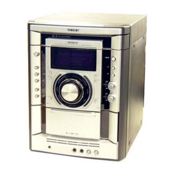
Sony HCD-LX10000 Service Manual
Hide thumbs
Also See for HCD-LX10000:
- Operating instructions manual (40 pages) ,
- Specification sheet (2 pages) ,
- Limited warranty (1 page)
Table of Contents
Advertisement
SERVICE MANUAL
Ver. 1.1 2008.01
• HCD-LX10000 is the Amplifier,
CD player, tape deck and tuner
section in MHC-LX10000.
AUDIO POWER SPECIFICATION
POWER OUTPUT AND TOTAL HARMONIC
DISTORTION:
With 6-ohm loads, both channels driven, from120 Hz – 10 kHz; rates 230
watts per channelminimum RMS power, with no more than 10% total
harmonic distortion from 250 miliwatts to rated output.
Amplifier section
Total harmonic distortion
Inputs
VIDEO/MD (AUDIO) IN (phono jacks):
TV (AUDIO) IN (phono jack):
MIC (phone jack):
Outputs
PHONES (stereo mini jack):
FRONT SPEAKER:
SURROUND SPEAKER:
Disc player section
System
Laser
Laser Output
9-887-216-02
Sony Corporation
2008A04-1
Audio Business Group
Published by Sony Techno Create Corporation
© 2008.01
HCD-LX10000
Model Name Using Similar Mechanism
CD
CD Mechanism Type
Section
Base Unit Name
Optical Pick-up Name
TAPE
Model Name Using Similar Mechanism
Section
Tape Transport Mechanism Type
SPECIFICATIONS
Less than 0.1%
(6 ohms at 1 kHz, 100 W)
voltage 250/450 mV,
impedance 47 kiloohms
voltage 250 mV,
impedance 47 kiloohms
sensitivity 1 mV,
impedance 10 kiloohms
accepts headphones of
8 ohms or more
Use only the supplied speaker
Use only the supplied speaker
Compact disc and digital
audio system
Semiconductor laser
(λ=780 nm)
Emission duration:
continuous
Max. 44.6 µW*
*This output is the value
MiNi Hi-Fi COMPONENT SYSTEM
measured at a distance of
200 mm from the objective
Frequency response
Signal-to-noise ratio
Dynamic range
Tape deck section
Recording system
Frequency response
Tuner section
FM stereo, FM/AM superheterodyne tuner
FM tuner section
Tuning range
Antenna
Antenna terminals
Intermediate frequency
AM tuner section
Tuning range
Antenna
Antenna terminals
Intermediate frequency
US Model
HCD-GX9900
CDM74-F1BD81
BU-F1BD81A
KSM-215DCP/C2NP
HC-GX9900
CMAT5Z2
lens surface on the Optical
Pick-up Block with 7 mm
aperture.
2 Hz – 20 kHz (±0.5 dB)
Wave length 780 – 790 nm
More than 90 dB
More than 90 dB
4-track 2-channel stereo
50 – 13,000 Hz (±3 dB),
using Sony TYPE I tape
87.5 – 108.0 MHz
FM lead antenna
75 ohm unbalanced
10.7 MHz
530 – 1,710 kHz
(with the interval set at 10kHz)
531 – 1,710 kHz
(with the interval set at 9 kHz)
AM loop antenna
External antenna terminal
450 kHz
– Continued on next page –
Advertisement
Table of Contents

Related Manuals for Sony HCD-LX10000


Summary of Contents for Sony HCD-LX10000
- Page 1 HCD-LX10000 SERVICE MANUAL US Model Ver. 1.1 2008.01 • HCD-LX10000 is the Amplifier, CD player, tape deck and tuner section in MHC-LX10000. Model Name Using Similar Mechanism HCD-GX9900 CD Mechanism Type CDM74-F1BD81 Section Base Unit Name BU-F1BD81A Optical Pick-up Name...
-
Page 2: Leakage Test
LIST ARE CRITICAL TO SAFE OPERATION. REPLACE THESE • Usable with ordinary solder COMPONENTS WITH SONY PARTS WHOSE PART NUMBERS It is best to use only unleaded solder but unleaded solder may APPEAR AS SHOWN IN THIS MANUAL OR IN SUPPLEMENTS also be added to ordinary solder. -
Page 3: Table Of Contents
HCD-LX10000 TABLE OF CONTENTS DIAGRAMS ..............25 SERVICING NOTES ..........4 7-1. Circuit Boards Location ..........26 7-2. Block Diagram – CD Section – ........27 GENERAL 7-3. Block Diagram – Tape/Tuner Section – ......28 Location of Controls ............5 7-4. -
Page 4: Servicing Notes
HCD-LX10000 SECTION 1 SERVICING NOTES NOTES ON HANDLING THE OPTICAL PICK-UP BLOCK OR BASE UNIT The laser diode in the optical pick-up block may suffer electrostatic break-down because of the potential difference generated by the charged electrostatic load, etc. on clothing and the human body. -
Page 5: General
HCD-LX10000 SECTION 2 GENERAL This section is extracted from instruction manual. LOCATING THE CONTROLS List of button locations ALPHABETICAL ORDER SYMBOLS M - R MASTER VOLUME 4 ?/1 (power) ej A - D MIC 1 (jack) wd Z OPEN/CLOSE 3 ALBUM +/−... -
Page 6: Remote Control
HCD-LX10000 This section is extracted from instruction manual. Remote control TAPE wd ALPHABETICAL ORDER TUNER/BAND 7 TUNER MEMORY wg A - E TUNING MODE 5 ALBUM + qf VOLUME +/− qg ALBUM − qh The + button has a tactile dot.*... -
Page 7: Disassembly
HCD-LX10000 SECTION 3 DISASSEMBLY • This set can be disassembled in the order shown below. 3-1. DISASSEMBLY FLOW 3-2.SIDE PANEL, TOP CASE (Page 8) 3-3.LOADING PANEL ASSY (Page 8) 3-4.FRONT PANEL ASSY (Page 9) 3-7.PANEL BOARD, 3-6.TAPE MECHANISM DECK, 3-5.TUNER PACK... -
Page 8: Side Panel, Top Case
HCD-LX10000 Note: Follow the disassembly procedure in the numerical order given. 3-2. SIDE PANEL, TOP CASE qd CASE (TOP) 7 two screws (case 3 TP2) 8 two screws (3 × 12) (+BVTP 3 × 10) qa two screws (+BVTP 3 × 10) -
Page 9: Front Panel Assy
HCD-LX10000 3-4. FRONT PANEL ASSY 7 connector (CN100) 9 CNP509 8 CNP508 4 screw (+BVTP 3 × 10) 3 screw (+BVTP 3 × 10) qa connector 6 front panel assy (CN1102) q; connector (CN503) 5 screw qs connector (+BVTP 3 × 6) -
Page 10: Tape Mechanism Deck, Mic Board
HCD-LX10000 3-6. TAPE MECHANISM DECK, MIC BOARD 2 cover (TCM) 1 four screws 3 screw (+BVTP2.6 (3CR)) (+BVTP2.6 (3CR)) 4 tape mechanism deck 5 two screws (+BVTP2.6 (3CR)) 6 bracket (MIC) 8 MIC board 7 two knobs (MIC) 3-7. PANEL BOARD, CD-SW BOARD 7 three screws (+BVTP2.6 (3CR)) -
Page 11: Cd Mechanism Deck
HCD-LX10000 3-8. CD MECHANISM DECK 2 CD mechanism deck 3 CNP505 1 screw (+BVTP 3 × 10) 4 connector (CN701) 3-9. BACK PANEL 7 back panel 3 connector 2 connector (CN01) (CN1204) 6 two screws (+BVTP 3 × 10) 1 connector... -
Page 12: Primary Board, Lighting Board
HCD-LX10000 3-10. PRIMARY BOARD, LIGHTING BOARD 1 connector (CN101) 5 two screws (+BVTP 3 × 10) 4 PRIMARY board 2 connector 3 screw (CN201) (+BVTP 3 × 8) 6 LIGHTING board 3-11. POWER AMP PC BOARD ASSY, MAIN BOARD 5 screw 4 two screws (+BVTP 3 ×... -
Page 13: Surround Board, Pa Board
HCD-LX10000 3-12. SURROUND BOARD, PA BOARD 2 SURROUND board 1 two screws (+BVTP 3 × 10) 8 heat sink 3 two screws (+BVTP 3 × 10) q; bracket 9 screw (+BVTP 3 × 10) 4 holder qa PA board 6 two screws... -
Page 14: Driver Board, Sw Board
HCD-LX10000 3-14. DRIVER BOARD, SW BOARD 3 two screws 2 cover (CDM) (+BTTP (M2.6)) 1 three screws (+BVTP 3 × 10) 5 connector (CN703) 6 DRIVER board 7 screw (+BTTP (M2.6)) 8 SW board 4 wire (flat type) (CN702) 3-15. CD BOARD, OPTICAL PICK-UP (KSM-215DCP/C2NP) qg Remove the four solderings of motor. -
Page 15: Sensor Board
HCD-LX10000 3-16. SENSOR BOARD 1 floating screw (+PTPWH M2.6) 2 t ray 8 s crew (+BTTP (M2.6)) 3 b elt (table) 0 SENSOR board 4 floating screw (+PTPWH M2.6) 5 p ulley (table) 9 connector 6 floating screw ( CN731) (+PTPWH M2.6) -
Page 16: Motor (Ld) Board
HCD-LX10000 3-18. MOTOR (LD) BOARD 3 two screws (+BTTP (M2.6)) 2 Remove the two solderings of motor. 4 MOTOR (LD) board 5 l oading motor assy (M751) 1 b elt (loading) -
Page 17: Test Mode
HCD-LX10000 SECTION 4 TEST MODE [GC TEST MODE] [MC TEST MODE] • This mode is used to check the fluorescent indicator tube, • This mode is used to check operations of the respective sections LEDs, keys, MASTER VOLUME jog, OPERATION of Amplifier and Tape. - Page 18 HCD-LX10000 [VACS ON/OFF] [AGING MODE] • This mode is used to switch ON and OFF the VACS (Variable This mode can be used for operation check of CD section. Attenuation Control System). • If an error occurs, the aging operation would stops and the status is displayed.
- Page 19 HCD-LX10000 • Display when an error occurred (CD Error Code Mode) 3) Display of no disc errors Procedure: Display 1. Press x button, [ENTER] button and [DISC 1] button simultaneously to enter the error code display mode. D*$$%%&&##00 2. The fluorescent indicator tube displays the number of total error.
- Page 20 HCD-LX10000 [CD SHIP MODE (WITHOUT MEMORY CLEAR)] [CD TRAY LOCK MODE] • This mode moves the optical pick-up to the position durable • This mode let you lock the disc tray. When this mode is to vibration. Use this mode when returning the set to the...
-
Page 21: Mechanical Adjustments
HCD-LX10000 SECTION 5 SECTION 6 MECHANICAL ADJUSTMENTS ELECTRICAL ADJUSTMENTS Precaution DECK SECTION 0 dB=0.775 V 1. Clean the following parts with a denatured alcohol-moistened swab: 1. Demagnetize the record/playback head with a head record/playback heads pinch rollers demagnetizer. erase head rubber belts 2. -
Page 22: Cd Section
HCD-LX10000 2. Turn the adjustment screw and check output peaks. If the peaks CD SECTION do not match for L-CH and R-CH, turn the adjustment screw so that outputs match within 1dB of peak. Note: 1. CD Block is basically designed to operate without adjustment. - Page 23 HCD-LX10000 RFAC Level Check E-F Balance Check Connection: Connection: oscilloscope oscilloscope CD board CD board TPO103 (TE1) TP124 (RFAC) TP117 (VC) TP117 (VC) – – Procedure: Procedure: 1. Connect an oscilloscope to test point TP124 (RFAC) and TP 1. Connect an oscilloscpe to test point TPO103 (TE1) and TP117 117(VC) on the CD board.
- Page 24 HCD-LX10000 Checking Location: – CD BOARD (SIDE B) – TP117 (VC) JPO103 (TE1) IC101 JPO102 (FE1) TP124 (RFAC)
-
Page 25: Diagrams
HCD-LX10000 SECTION 7 DIAGRAMS Note on Printed Wiring Boards: For schematic diagrams. Note: Note: • All capacitors are in µF unless otherwise noted. (p: pF) • X : parts extracted from the component side. 50 V or less are not indicated except for electrolytics and •... -
Page 26: Circuit Boards Location
HCD-LX10000 7-1. CIRCUIT BOARDS LOCATION PRIMARY board CD-SW board TUNER PACK LIGHTING board TRANS board SWITCHING POWER SURROUND board PA board SENSOR board SW board CD board MOTOR (TB) board MOTOR (LD) board DRIVER board PANEL board JOG board MAIN board... -
Page 27: Block Diagram - Cd Section
HCD-LX10000 7-2. BLOCK DIAGRAM – CD SECTION – MAIN CD-L AOUT1 SECTION (Page 29) AOUT2 R-CH OPTICAL PICK-UP BLOCK IC101 CD MUTE CD MUTE DRIVE (KSM-215DCP/C2NP) Q250,251 Q540, 541 RF AMP, DSP,DAC DETECTOR +3.3V IC301 MP3 DECODER IC303 PCMD1 SDO0 +3.3V... -
Page 28: Block Diagram - Tape/Tuner Section
HCD-LX10000 7-3. BLOCK DIAGRAM – TAPE/TUNER SECTION – DECK-A AIN1 L – CH MAIN EQ OUT1 TC-PB-L PB OUT1 TAI1 HEAD SECTION (Page 29) R – CH R-CH CN510 BIN1 MUTE SWITCH Q280 DRIVE R-CH TEST DECK-B Q382, 383 Q376... -
Page 29: Block Diagram - Main Section
HCD-LX10000 7-4. BLOCK DIAGRAM – MAIN SECTION – J1100(1/3) MIC 1 RV1100 MIC LEVEL J1101(1/3) REC-OUT-L TAPE/TUNER IC1100 (1/2) IC1100 (2/2) MIC OUT SECTION MIC 2 MIC AMP MIC AMP (Page 28) J1100(2/3) J1100(3/3) J1101(3/3) J1101(2/3) IC1101 LPF1 LPF2 DIGTAL... -
Page 30: Block Diagram - Amp Section
HCD-LX10000 7-5. BLOCK DIAGRAM – AMP SECTION – MAIN DBFB F/B J1103 SECTION (Page 29) PHONES IC600 POWER AMP D624 TM600 MAIN SECTION (Page 29) FRONT SPEAKER RY646 OVER LOAD TM601 DETECT MUTING Q668, 618 TH629 Q604, 606, 610 MUTING... -
Page 31: Block Diagram - Display/Power Section
HCD-LX10000 7-6. BLOCK DIAGRAM – DISPLAY/POWER SECTION – LED+9V KEY2 S1149-1160 83 XIN S910,911,918,920,924 X901 KEY0 S901 – 904, 912,915,917 4MHz 82 XOUT Q905 Q907 Q906 P1 – 36 SELECTOR Q904 P1 – 36 IC902 DISPLAY CONTROL FL901 KEY CONTROL... -
Page 32: Printed Wiring Board - Cd Board
HCD-LX10000 7-7. PRINTED WIRING BOARD – CD BOARD – • See page 26 for Circuit Boards Location. : Uses unleaded solder. CD BOARD (SIDE A) CD BOARD (SIDE B) M101 (SPINDLE) M102 (SLED) MAIN BOARD CN505 (Page 36) 1-860-502- (13) -
Page 33: Schematic Diagram - Cd Board
HCD-LX10000 7-8. SCHEMATIC DIAGRAM – CD BOARD – • See pages 48 and 49 for IC Block Diagrams. • See page 48 for Waveforms. • See page 50 for IC Pin Function Description. CN101 R307 C125 C134 C307 TP304 C151... -
Page 34: Printed Wiring Boards - Cd Mechanism Boards
HCD-LX10000 7-9. PRINTED WIRING BOARDS – CD MECHANISM BOARDS – • See page 26 for Circuit Boards Location. : Uses unleaded solder. MAIN BOARD NO507 (Page 36) CN751 S751 (OPEN) • Semiconductor Location Ref. No. Location D701 D711 IC701 IC712... -
Page 35: Schematic Diagram - Cd Mechanism Boards
HCD-LX10000 7-10. SCHEMATIC DIAGRAM – CD MECHANISM BOARDS – • See page 48 for IC Block Diagrams. HCD-LX10000... -
Page 36: Printed Wiring Board - Main Board
HCD-LX10000 7-11. PRINTED WIRING BOARD – MAIN BOARD – • See page 26 for Circuit Boards Location. : Uses unleaded solder. DRINER TUNER BOARD BOARD PACK (FOR CHECK) CN201 CN701 PRIMARY (Page 32) MAIN BOARD (Page 34) BOARD BOARD CN1200... -
Page 37: Schematic Diagram - Main Board (1/3)
HCD-LX10000 7-12. SCHEMATIC DIAGRAM – MAIN BOARD (1/3) – • See page 48 for Waveforms. • See page 53 for IC Pin Function Description. HCD-LX10000... -
Page 38: Schematic Diagram - Main Board (2/3)
HCD-LX10000 7-13. SCHEMATIC DIAGRAM – MAIN BOARD (2/3) – HCD-LX10000... -
Page 39: Schematic Diagram - Main Board (3/3)
HCD-LX10000 7-14. SCHEMATIC DIAGRAM – MAIN BOARD (3/3) – • See page 48 for Waveforms. HCD-LX10000... -
Page 40: Printed Wiring Board - Panel Board
HCD-LX10000 7-15. PRINTED WIRING BOARD – PANEL BOARD – • See page 26 for Circuit Boards Location. : Uses unleaded solder. PANEL BOARD • Semiconductor Location DISPLAY CD SYNC CD-SW Ref. No. Location BOARD TUNER D901 B-10 NO1150 BAND D902... -
Page 41: Schematic Diagram - Panel Board
HCD-LX10000 7-16. SCHEMATIC DIAGRAM – PANEL BOARD – • See page 48 for IC Block Diagrams. • See page 48 for Waveforms. • See page 55 for IC Pin Function Description. HCD-LX10000... -
Page 42: Printed Wiring Boards - Cd-Sw, Jog, Mic, Lighting Boards
HCD-LX10000 7-17. PRINTED WIRING BOARDS – CD-SW, JOG, MIC, LIGHTING BOARDS – • See page 26 for Circuit Boards Location. : Uses unleaded solder. CD-SW BOARD PANEL BOARD NO903 (Page 40) EX-CHANGE/ Z OPEN/CLOSE DISC 2 DISC 1 DISC 3... -
Page 43: Schematic Diagram - Cd-Sw, Jog, Mic, Lighting Boards
HCD-LX10000 7-18. SCHEMATIC DIAGRAM – CD-SW, JOG, MIC, LIGHTING BOARDS – MAIN BOARD (2/3) (Page 38) HCD-LX10000... -
Page 44: Printed Wiring Board - Pa Board
HCD-LX10000 7-19. PRINTED WIRING BOARD – PA BOARD – • See page 26 for Circuit Boards Location. : Uses unleaded solder. MAIN MAIN BOARD BOARD BOARD CN502 CN501 CN1102 (Page 36) (Page 36) (Page 42) PA BOARD FRONT SPEAKER SURR SPEAKER –... -
Page 45: Schematic Diagram - Pa Board
HCD-LX10000 7-20. SCHEMATIC DIAGRAM – PA BOARD – HCD-LX10000... -
Page 46: Printed Wiring Boards - Trans, Primary Boards
HCD-LX10000 7-21. PRINTED WIRING BOARDS – TRANS, PRIMARY BOARDS – • See page 26 for Circuit Boards Location. : Uses unleaded solder. T1200 TRANS BOARS POWER TRANSFORMER BOARD NO600 (Page 44) MAIN BOARD NO503 (Page 36) NOT REPLACEABLE: BUILT IN TRANSFORMER... -
Page 47: Schematic Diagram - Trans, Primary Boards
HCD-LX10000 7-22. SCHEMATIC DIAGRAM – TRANS, PRIMARY BOARDS – HCD-LX10000... - Page 48 HCD-LX10000 • IC Block Diagram • WAVEFORMS – CD BOARD – – MAIN BOARD – – PANEL BOARD – – DRIVER Board – – PANEL Board – IC701, 712 BA6956AN IC904 NJM2760V-TE2 IC101 wa IC401 qa IC902 is XC-OUT X OUT...
- Page 49 HCD-LX10000 – CD Board – IC301 TC94A34FG-002 LRCKIA CS/RAS/ADO2 AD15/CAS/PD12 BCKIA SDO3/OE SDI0 PO11/BUCK/AD14 LRCKO PO10/CCE/AD13 BCKO PO9/AD12 SDO0 PO08/AD11 VDDM VDDT SRMSTB MIACK MICK VDDT AD10 MIDIO MILP Switch MICS STANBY PO07/AD7 RESET PO06/AD6 VDDP PO05/AD5 Timing Generator...
-
Page 50: Ic Pin Function Description
HCD-LX10000 7-23. IC Pin Function Descriptions • IC101 CXD3059AR (RF AMP, DSP, DAC) (CD BOARD) Pin No. Pin Name Description MIRR Not used (Open) DFCT Not used (Open) Not used (Open) — Ground LOCK Not used (Open) Spindle motor servo control output... - Page 51 HCD-LX10000 Pin No. Pin Name Description AVSS3 — Ground CLTV Multiplier VCO1 control voltage input FILO Master PLL (slave = digital PLL) filter output FILI Master PLL filter input Master PLL charge pump output AVDD5 — Power supply (+3.3V) DDVROUT DC/DC converter output (+2.5V)
- Page 52 HCD-LX10000 Pin No. Pin Name Description EXCK Not used (Open) XRST System reset input from M30622MEP SYSM Mute input (Connected to ground) DATA Serial data input from M30622MEP — ground XLAT Latch input from M30622MEP CLOCK Serial data transfer clock input from M30622MEP —...
- Page 53 HCD-LX10000 • IC401 M30622MEP-A77FPU0 SYSTEM CONTROL (MAIN BOARD) Pin No. Pin Name Description XRST Reset signal output to CXD3053AR CD-DATA Serial data output to CXD3053AR XLAT Serial data latch signal output to CXD3053AR SIRCS Remote control signal input MP3 DATA OUT...
- Page 54 HCD-LX10000 Pin No. Pin Name Description SW LED2 Not used (Open) B-PLAY Deck B playback detection signal input THERMAL VACS Thermal VACS detection input A-TRIG Deck A side trigger plunger drive signal output CAPM-CONT Capstan motor drive signal output B-TRIG...
- Page 55 HCD-LX10000 • IC902 MB90M407PF-G-144E1 DISPLAY CONTROL (PANEL Board) Pin No. Pin Name Description 1 to 8 G8 to G1 FLD grid signal output 9, 10 P1,P2 FLD segment signal output VSS-IO — Ground 12 to 22 P3 to P13 FLD segment signal output VDD-FIP —...
-
Page 56: Exploded Views
HCD-LX10000 SECTION 8 EXPLODED VIEWS NOTE: • -XX, -X mean standardized parts, so they may • Hardware (# mark) list and accessories are The components identified by mark 0 or have some differences from the original one. given in the last of this parts list. -
Page 57: Front Panel Section
HCD-LX10000 8-2. FRONT PANEL SECTION not supplied FL901 not supplied not supplied not supplied not supplied not supplied 52 53 Ref. No. Part No. Description Remarks Ref. No. Part No. Description Remarks X-2025-429-1 FRONT PANEL ASSY X-2025-430-1 KNOB JOG ASSY... -
Page 58: Chassis Section
HCD-LX10000 8-3. CHASSIS SECTION not supplied not supplied not supplied F1281 F1271 F1241 F1261 F1251 T1200 not supplied Ref. No. Part No. Description Remarks Ref. No. Part No. Description Remarks 4-900-386-01 SCREW A-1189-960-A MAIN BOARD, COMPLETE A-1089-586-A PA BOARD, COMPLETE... -
Page 59: Cd Mechanism Deck Section-1 (Cdm74-F1Bd81)
HCD-LX10000 8-4. CD MECHANISM DECK SECTION-1 (CDM74-F1BD81) M741 CD mechanism deck section-2 Ref. No. Part No. Description Remarks Ref. No. Part No. Description Remarks 4-243-820-01 GEAR (TABLE) 4-218-253-32 SCREW (M2.6), +BTTP 1-776-182-11 WIRE (FLAT TYPE) (5 CORE) 4-243-819-01 GEAR (GENEVA) -
Page 60: Cd Mechanism Deck Section-2 (Cdm74-F1Bd81)
HCD-LX10000 8-5. CD MECHANISM DECK SECTION-2 (CDM74-F1BD81) RE701 M751 not supplied Ref. No. Part No. Description Remarks Ref. No. Part No. Description Remarks 1-687-135-12 DRIVER BOARD X-4955-774-2 PULLEY (SM) ASSY, CHUCKING 4-218-253-52 SCREW (M2.6), +BTTP 4-221-688-01 PULLEY (B), CHUCKING 1-687-669-12 SW BOARD... -
Page 61: Electrical Parts List
HCD-LX10000 SECTION 9 ELECTRICAL PARTS LIST NOTE: • Due to standardization, replacements in the • COILS The components identified by mark 0 uH: µH parts list may be different from the parts or dotted line with mark 0 are critical specified in the diagrams or the components •... - Page 62 HCD-LX10000 CD-SW DRIVER Ref. No. Part No. Description Remarks Ref. No. Part No. Description Remarks < IC > R404 1-216-809-11 METAL CHIP 1/10W R405 1-216-809-11 METAL CHIP 1/10W IC101 8-752-425-12 IC CXD3059AR R406 1-216-809-11 METAL CHIP 1/10W IC251 6-705-808-01 IC BA5947FM-E2...
- Page 63 HCD-LX10000 DRIVER LIGHTING MAIN Ref. No. Part No. Description Remarks Ref. No. Part No. Description Remarks < IC > R1146 1-216-820-11 METAL CHIP 1/10W IC701 8-759-598-69 IC BA6956AN R1156 1-216-821-11 METAL CHIP 1/10W IC712 8-759-598-69 IC BA6956AN R1157 1-216-820-11 METAL CHIP...
- Page 64 HCD-LX10000 MAIN Ref. No. Part No. Description Remarks Ref. No. Ref. No. Part No. Part No. Description Description Remarks Remarks C111 1-126-964-11 ELECT 10uF C370 1-137-150-11 FILM 0.01uF 100V C112 1-136-170-00 FILM 0.27uF C371 1-162-968-11 CERAMIC CHIP 0.0047uF 10% C113 1-136-170-00 FILM 0.27uF...
- Page 65 HCD-LX10000 MAIN Ref. No. Part No. Description Remarks Ref. No. Part No. Description Remarks C560 1-130-483-00 MYLAR 0.01uF C561 1-130-483-00 MYLAR 0.01uF < IC > C562 1-126-933-11 ELECT 100uF C563 1-126-925-91 ELECT 470uF IC101 6-703-650-11 IC M61529FP-D60G C564 1-100-566-91 CERAMIC CHIP 0.1uF...
- Page 66 HCD-LX10000 MAIN Ref. No. Part No. Description Remarks Ref. No. Part No. Description Remarks < TRANSISTOR > R130 1-216-825-11 METAL CHIP 2.2K 1/10W R131 1-216-825-11 METAL CHIP 2.2K 1/10W Q101 8-729-120-28 TRANSISTOR 2SC1623-L5L6 R132 1-216-857-11 METAL CHIP 1/10W Q151 8-729-120-28 TRANSISTOR 2SC1623-L5L6...
- Page 67 HCD-LX10000 MAIN Ref. No. Part No. Description Remarks Ref. No. Part No. Description Remarks R302 1-216-829-11 METAL CHIP 4.7K 1/10W R394 1-216-829-11 METAL CHIP 4.7K 1/10W R303 1-216-833-11 METAL CHIP 1/10W R395 1-216-841-11 METAL CHIP 1/10W R396 1-216-833-11 METAL CHIP...
- Page 68 HCD-LX10000 MAIN Ref. No. Part No. Description Remarks Ref. No. Part No. Description Remarks R486 1-216-809-11 METAL CHIP 1/10W C1101 1-162-970-11 CERAMIC CHIP 0.01uF R487 1-216-809-11 METAL CHIP 1/10W C1102 1-124-257-00 ELECT 2.2uF C1103 1-162-923-11 CERAMIC CHIP 47PF R488 1-216-809-11 METAL CHIP...
- Page 69 HCD-LX10000 MOTOR (LD) MOTOR (TB) Ref. No. Part No. Description Remarks Ref. No. Part No. Description Remarks JR1102 1-216-864-11 SHORT CHIP < CAPACITOR > JR1103 1-216-296-11 SHORT CHIP JR1104 1-216-296-11 SHORT CHIP C600 1-126-963-11 ELECT 4.7uF JR1105 1-216-296-11 SHORT CHIP...
- Page 70 HCD-LX10000 Ref. No. Part No. Description Remarks Ref. No. Part No. Description Remarks < IC > R630 1-216-845-11 METAL CHIP 100K 1/10W R631 1-216-845-11 METAL CHIP 100K 1/10W IC600 8-749-017-06 IC STK412-150 R632 1-216-845-11 METAL CHIP 100K 1/10W R633 1-216-842-11 METAL CHIP 1/10W <...
- Page 71 HCD-LX10000 PANEL Ref. No. Part No. Description Remarks Ref. No. Part No. Description Remarks < RELAY > C947 1-125-837-91 CERAMIC CHIP 6.3V C948 1-164-315-11 CERAMIC CHIP 470PF RY646 1-755-500-11 RELAY RY665 1-755-500-11 RELAY C949 1-125-837-91 CERAMIC CHIP 6.3V C950 1-162-968-11 CERAMIC CHIP 0.0047uF 10%...
- Page 72 HCD-LX10000 PANEL Ref. No. Part No. Description Remarks Ref. No. Part No. Description Remarks < FERRITE BEAD > R910 1-216-821-11 METAL CHIP 1/10W FB901 1-216-864-11 SHORT CHIP R911 1-216-821-11 METAL CHIP 1/10W R912 1-216-809-11 METAL CHIP 1/10W < FLUORESCENT INDICATOR >...
- Page 73 HCD-LX10000 PANEL PRIMARY SENSOR Ref. No. Part No. Description Remarks Ref. No. Part No. Description Remarks R987 1-216-819-11 METAL CHIP 1/10W S917 1-771-963-11 SWITCH, ROTARY (ALBUM) R988 1-216-819-11 METAL CHIP 1/10W S918 1-762-875-21 SWITCH, KEYBOARD (TAPE A/B) R989 1-216-819-11 METAL CHIP...
- Page 74 HCD-LX10000 SENSOR SURROUND TRANS Ref. No. Part No. Description Remarks Ref. No. Part No. Description Remarks < IC > 0F1241 1-576-537-12 FUSE, GLASS TUBE (DIA.5) (T8AL/125V) 0F1251 1-576-537-12 FUSE, GLASS TUBE (DIA.5) (T8AL/125V) IC731 6-600-022-01 IC RPI-576 0F1261 1-576-537-12 FUSE, GLASS TUBE (DIA.5) (T8AL/125V) 0F1271 1-576-537-12 FUSE, GLASS TUBE (DIA.5) (T8AL/125V)
- Page 75 HCD-LX10000 US Model SERVICE MANUAL Ver. 1.1 2008.01 SUPPLEMENT-1 File this supplement with the service manual. Subject: Specification change Specification changes made for serial No. 8891860 and later. Check the serial No. when servicing and inspecting the set. This service manual, SUPPLEMENT-1 only contains the change.
- Page 76 HCD-LX10000 For schematic diagrams. Note on Printed Wiring Boards: Note: Note: • All capacitors are in µF unless otherwise noted. (p: pF) • X : parts extracted from the component side. 50 V or less are not indicated except for electrolytics and •...
- Page 77 HCD-LX10000 1. PRINTED WIRING BOARD – PA Board – : Uses unleaded solder. MAIN MAIN BOARD BOARD BOARD CN502 CN1102 CN501 <Page 36> <Page 42> <Page 36> PA BOARD FRONT SPEAKER SURR SPEAKER – – • Semiconductor Location Ref. No.
- Page 78 HCD-LX10000 2. SCHEMATIC DIAGRAM – PA Board – <Page 47> <Page 43> <Page 39> <Page 39> HCD-LX10000...
- Page 79 HCD-LX10000 3. EXPLODED VIEWS NOTE: The components identified by mark • -XX, -X mean standardized parts, so they may • The mechanical parts with no reference 0 or dotted line with mark 0 are have some differences from the original one.
- Page 80 HCD-LX10000 (2) FRONT PANEL SECTION not supplied FL901 not supplied not supplied not supplied not supplied 52 53 Ref. No. Part No. Description Remark Ref. No. Part No. Description Remark X-2025-429-1 FRONT PANEL ASSY X-2025-430-1 KNOB JOG ASSY 2-342-128-01 ESCUTHEON (LID)
- Page 81 HCD-LX10000 (3) CHASSIS SECTION not supplied not supplied D658 D656 not supplied F1281 F1271 F1241 F1261 F1251 T1200 not supplied Ref. No. Part No. Description Remark Ref. No. Part No. Description Remark 0 F1241 4-900-386-01 SCREW 1-576-537-12 FUSE, GLASS TUBE (DIA.5) (T8AL/125V)
- Page 82 HCD-LX10000 4. ELECTRICAL PARTS LIST NOTE: The components identified by mark • Due to standardization, replacements in the • Items marked “*” are not stocked since they 0 or dotted line with mark 0 are parts list may be different from the parts are seldom required for routine service.
- Page 83 HCD-LX10000 Ref. No. Part No. Description Remark Ref. No. Part No. Description Remark R601 1-216-841-11 METAL CHIP 1/10W R660 1-216-837-11 METAL CHIP 1/10W R602 1-216-819-11 METAL CHIP 1/10W R661 1-216-837-11 METAL CHIP 1/10W R603 1-216-841-11 METAL CHIP 1/10W R662 1-216-811-11 METAL CHIP...
- Page 84 HCD-LX10000 Ref. No. Part No. Description Remark MISCELLANEOUS *************** 1-693-672-11 TUNER (FM/AM) (TM-10U) 1-468-737-71 SWITCHING, POWER 1-824-048-12 WIRE (FLAT TYPE) (27 CORE) 1-828-992-11 WIRE (FLAT TYPE) (17 CORE) 1-797-165-11 DECK, MECHANICAL (CMAT5Z2) 1-828-956-11 WIRE (FLAT TYPE) (9 CORE) 0 107...
- Page 85 HCD-LX10000 MEMO...
-
Page 86: Revision History
HCD-LX10000 REVISION HISTORY Clicking the version allows you to jump to the revised page. Also, clicking the version at the top of the revised page allows you to jump to the next revised page. Ver. Date Description of Revision 2006.04 2008.01...
Need help?
Do you have a question about the HCD-LX10000 and is the answer not in the manual?
Questions and answers
This model of Sony sound broad system speaker output pin names please