
Related Manuals for Standart HX290UKA


Summary of Contents for Standart HX290UKA
- Page 1 Hand held Transceiver HX290U ( KA ) HX290UKA131 / 191 / 181 / 111 SERVICE MANUAL Copyright © 1999 Marantz Japan, Inc All Rights Reserved Printed in Japan...
-
Page 2: Table Of Contents
3.1 Removing the Diecast frame ............................11 3.2 Removing the TX/RX/CONTROL P.C.board........................12 4. ADJUSTMENT..................................13 4.1 Adjustment Connection Diagrams..........................16 4.2 Adjustment Point Diagrams............................17 4.3 HX290UKA Adjustment and Confirmation ........................18 4.3.1 PLL Block ................................18 4.3.2 Transmitter Block ..............................18 4.3.3 Receiver Block ................................19 5. SPECIFICATIONS ..................................21 6. -
Page 3: Controls And Connections
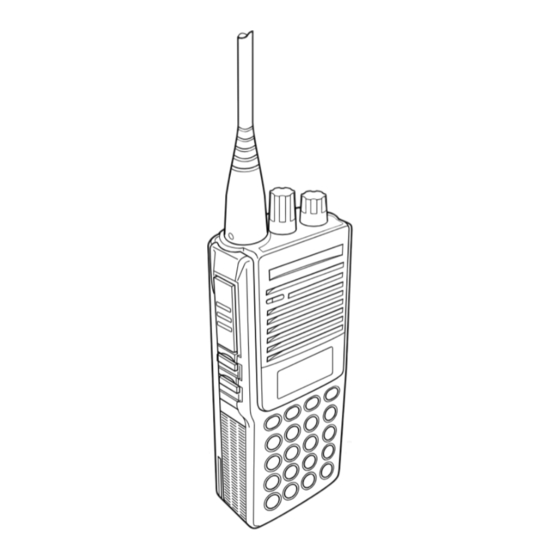
1. CONTROLS AND CONNECTIONS TX/BUSY HX290 DIAL Figure 1-1 u u LAMP key (power / volume) knob i i SCN (scan) key w w CH (channel) knob o o DIAL key e e TX/BUSY Indicator ! ! 0 0 T/A (Talkaround) key r r Antenna connector ! ! 1 1 H/L (high/low) key t t PTT switch... -
Page 4: Theory Of Operations
2. THEORY OF OPERATIONS Note : Refer to the block diagrams (figure 2-1 through 2-8) in the text for the operations of the circuits. 2.1 PLL Block The PLL block comprises a VCO, TCXO, PLL IC, and PLL loop filter. The VCO circuit generates the transmission signal and first local signal directly. -
Page 5: Receiver Block
2.1.6 VCO Circuit level output. This high level output signal is input to an The DC voltage output by the PLL loop filter is input to a unlock switch QP04, causing it to turn on. When the variable capacitance diode built into the VCO. This DC unlock switch is on, a low level output signal is input to pin voltage changes the capacitance between the electrodes 37 of microprocessor QL02. - Page 6 2.2.4 Second IF Circuit The second IF IC comprises a second local oscillator, the first IF signal is converted into a 455 kHz second IF second mixer, second IF amplifier, wave detector, noise signal. After having adjacent signal elements eliminated amplifier, and noise wave detector.
-
Page 7: Transmitter Block
2.2.6 Squelch Circuit 2.2.7 Tone Decoder A portion of the audio signal output from pin 9 of second A portion of the audio signal output from pin 9 of second IF IC QH04 is input to a band-pass filter consisting of IF IC QH04 is input to tone detector circuit built into base CH23, RH22,CH30,RH14, CH21, CH22, RH12 and band IC QM01 as the tone signal. -
Page 8: Control Block
2.4 Control Block 2.4.1 Microprocessor QL02 The functions of the In / Out ports of microprocessor QL02 are listed below. Table 2-1 Port Name S.I/O S.PD Signal Name In/Out Active Initial P.UP/DN Function SEG05 SEG05 LCD segment output SEG06 SEG06 LCD segment output SEG07 SEG07... - Page 9 Port Name S.I/O S.PD Signal Name In/Out Active Initial P.UP/DN Function RSTX RESET (High) E-UP Reset input N.C. Sub clock connection terminal (N.C.) N.C. Sub clock connection (N.C.) MODA Operation mode specified (Vss) Main clock connection (9.8304 MHz) Main clock connection (9.8304 MHz) P80/INT24 CMOS CLK SHIFT...
- Page 10 2.4.2 Display (LCD) Microprocessor QL02 drives LCD QL01 directly. The driving method is dynamic drive using 24 segment terminals, two common terminals, and a 1/3 duty ratio. The LCD segment and common connections are illustrated below.(Figure2-7) SEGMENT COMMON Figure 2-7 LCD connection diagram...
-
Page 11: Power Supply Block
2.5 Power Supply Block The power supply block is diagrammed below.(Figure2-8) Power switch Fuse RA01 FA01 Vcc (7.2 V) QL05, QL03 Battery terminal QA02 DC 7.2 V QT03 pin 3 QT07 pin 8 5V regulator QL18 QL02 pin 47,30 QL17 QM01 pin 13 S81350HG QL10 pin10... -
Page 12: Disassembly
3. DISASSEMBLY Note : Be sure to switch off the transceiver's power before disassembling it. And then remove an antenna and a battery pack. 3.1 Removing the Diecast frame (d) Pull the diecast frame up from front case in the (a) Remove the single screw A to remove the Mic/Spk direction indicated by arrow q, and remove the it in jack cover. -
Page 13: Removing The Tx/Rx/Control P.c.board
3.2 Removing the TX/RX/CONTROL P.C.board (d) Remove the two screws E to remove the switching (a) Remove the frame packing. (b) Remove the two nuts D. plate and two clampers. (c) Remove the solder from area e on the TX/RX/CONTROL (e) Remove the three screws F. -
Page 14: Adjustment
4. ADJUSTMENT Make sure that all test equipment is properly calibrated. Allow sufficient time after powering on equipment for it to warm up before performing adjustments. - Standard conditions - Power supply voltage ............................DC 7.2 V Audio output ................................200 mW Audio load ..................................8 Ω... - Page 15 TX/RX adjustment frequencies – HX290UKA181 – Table 4-3 Channel RX frequency (Wide/Narrow) TX frequency (Wide/Narrow) Tone TX power 345.025 MHz (W) 345.100 MHz (W) None 357.525 MHz (W) 357.600 MHz (W) None 370.025 MHz (W) 370.100 MHz (W) None 345.0125 MHz (N) 345.100 MHz (N) None 357.5125 MHz (N)
- Page 16 (b) Turn on the power switch while holding down the DIAL key and LAMP key at the same time. At this point, the "Adj XX" (XX : channel number) indication on the LCD of the transceiver. - For the HX290UKA - Turn on the power switch while holding down the DIAL key and LAMP key at the same time.
-
Page 17: Adjustment Connection Diagrams
4.1 Adjustment Connection Diagrams Frequency Counter Deviation & Audio Generator AC Voltmeter Power Meter Directional Coupler RF Dummy Load (50 ohm) Oscilloscope Power Supply CAUTION : Use a microphone plug of the type shown below when adjusting the transmitter block. 10µF / 10V Microphone plug DC +7.2V... -
Page 18: Adjustment Point Diagrams
4.2 Adjustment Point Diagrams TX PLL lock TP (Test Point) P100 TX/RX/CONTROL P.C.Board voltage adj. CV04 CV14 RX PLL lock voltage adj. Tone deviation balance adj. RM52 RM50 Max. deviation adj. (Shown from solder side) P100 TX/RX/CONTROL P.C.Board TP (Test Point) (Shown from component side) Figure 4-5 Adjustment point diagram... -
Page 19: Hx290Uka Adjustment And Confirmation
4.3 HX290UKA Adjustment and Confirmation (f) At this point, adjust RM52 so that the waveform is a 4.3.1 PLL Block square wave. - Reception PLL lock voltage adjustment - (g) When the adjustment is complete, power off the (a) Set the transceiver channel to 02 and set the transceiver. -
Page 20: Receiver Block
(j) At this point, confirm that the CTCSS deviation is 4.3.3 Receiver Block between ± 0.35 kHz and ± 0.6 kHz - Reception sensitivity confirmation - (k) At this point, confirm that the TX frequency is between (a) Set the transceiver channel to 01. + 1 kHz and - 1 kHz. - Page 21 - Squelch sensitivity confirmation - (e) Input a 1 kHz, 1 Vp-p audio signal to pin 5 or 6 of JL04 (a) Press the MONI key twice within 1 second to set the from the audio generator. (AC connection by 0.1 µF) squelch level.
-
Page 22: Specifications
5. SPECIFICATIONS Frequency range F1...............................405MHz to 430 MHz F3..............................450 MHz to 470 MHz F9..............................370 MHz to 390 MHz F8..............................345 MHz to 370 MHz Number of channels..........................Max 100 channels Channel separation Wide ..................................25 kHz Narrow ..................................12.5 kHz Operation voltage range ..........................6.0 to 9.0 VDC Operation temperature range........................–... -
Page 23: Parts List
6. PARTS LIST Parts list The parts list contains information on electrical and mechanical parts. Electrical parts are listed first, followed by mechanical parts. Chip parts Part numbers whose first three characters correspond to the following codes indicate chip parts. -Capacitors- -Resistors- -Semiconductors-... - Page 24 Ref. Ref. Q'TY Part No. Description Desig. Q'TY Part No. Description Desig. P100 TX/RX/CONTROL P.C.BOARD P100 TX/RX/CONTROL P.C.BOARD P001 WI415B1002 TX/RX/CONTROL P.C.BOARD KIT CF21 DD95150300 15 pF ±5% P100 WI415B1012 TX/RX/CONTROL P.C.BOARD CF22 DK96103300 0.01 µF ±10% CF23 DD95101300 100 pF ±5% CA01 DK96102300...
- Page 25 Ref. Ref. Q'TY Part No. Description Desig. Q'TY Part No. Description Desig. P100 TX/RX/CONTROL P.C.BOARD P100 TX/RX/CONTROL P.C.BOARD CL31 DK96102300 1000 pF ±10% CP01 DD95470300 47 pF ±5% CL32 DK96473200 0.047 µF ±10% CP02 DD95470300 47 pF ±5% CL33 DK96102300 1000 pF ±10% CP03...
- Page 26 Ref. Ref. Q'TY Part No. Description Desig. Q'TY Part No. Description Desig. P100 TX/RX/CONTROL P.C.BOARD P100 TX/RX/CONTROL P.C.BOARD CT21 DD91090300 9 pF ±0.5 pF [F3][F9] JL01 YU01004700 LCD ZEBURA FCS-TYPE CT21 DD91100300 10 pF ±0.5pF [F8] JL02 YU08003700 SP ZEBURA GBU-TYPE CT21 DD95120300 12 pF...
- Page 27 Ref. Ref. Desig. Q'TY Part No. Description Desig. Q'TY Part No. Description P100 TX/RX/CONTROL P.C.BOARD P100 TX/RX/CONTROL P.C.BOARD LV01 LU04272010 MLF1608 2.7 µH ±10% QP01 HZ20060050 HN2D01FU LV02 LU28180010 LQN21A 18 nH ±5% [F1][F3] QP02 HC10133180 MB15E03 PLL-IC LV02 LU28220010 LQN21A 22 nH ±5% [F9][F8]...
- Page 28 Ref. Ref. Q'TY Part No. Description Q'TY Part No. Description Desig. Desig. P100 TX/RX/CONTROL P.C.BOARD P100 TX/RX/CONTROL P.C.BOARD RH07 NP05474610 470 kΩ ±5% 1/16W RL51 NP05102610 1 kΩ ±5% 1/16W RH08 NP05224610 220 kΩ ±5% 1/16W RL52 NP05102610 1 kΩ ±5% 1/16W RH09...
- Page 29 Ref. Ref. Desig. Q'TY Part No. Description Desig. Q'TY Part No. Description P100 TX/RX/CONTROL P.C.BOARD P100 TX/RX/CONTROL P.C.BOARD RM22 NP05473610 47 kΩ ±5% 1/16W RT01 NP05102610 1 kΩ ±5% 1/16W RM23 NP05472610 4.7 kΩ ±5% 1/16W RT02 NP05472610 4.7 kΩ ±5% 1/16W RM24...
- Page 30 Ref. Ref. Q'TY Part No. Description Desig. Q'TY Part No. Description Desig. MECHANISM MECHANISM 001B 408B064010 FRONT CASE 111B 408B107040 CU SHEET FOR DIE CAST FRAME 002B 408B270010 PTT BUTTON 112B 408B002020 SIDE CLAMPER (ANT SIDE) 003B 408B118010 SPACER FOR PTT BUTTON 113B 408B002030 SIDE CLAMPER (LAMP KEY SIDE)
-
Page 31: Exploded Parts View
7. EXPLODED PARTS VIEW 046B 201B J T01 101B 042B 035B QT03 034 B 043 B 045B x 2 112B 033B 032B 0 41B 106B 107B 070B 103 B 081B 111B S L0 1 RA0 1 115B 074B 111B 071B N L0 1 113B J L03... -
Page 32: Packing Diagram And Parts List
8. PACKING DIAGRAM AND PARTS LIST 009S 008S 004S 005S 001T V001 002S 001S 003S 002S HX290UKA131 19 <0076> 002S HX290UKA191 19 <0076> HX290UKA181 19 <0076> HX290UKA181 19 <0076> Ref. Ref. Q'TY Part No. Description Desig. Q'TY Part No. Description Desig. -
Page 33: Block Diagram
9. BLOCK DIAGRAM... -
Page 34: Schematic Diagram
10. SCHEMATIC DIAGRAM 10.1. HX290UKA131... -
Page 35: Hx290Uka191
10.2. HX290UKA191... -
Page 36: Hx290Uka181
10.3. HX290UKA181... -
Page 37: Hx290Uka111
10.4. HX290UKA111... -
Page 38: Component Overlay Diagram
11. COMPONENT OVERLAY DIAGRAM QL13,QL26 QL04,QL09 QL21,QL24 QL20 QL06 QL22 QL07 P100 TX/RX/CONTROL CL27 QL15 CL28 CL29 RL86 TEST RL84 RL85 POINT RL53 CL25 CL33 RL88 RL80 RL92 RL91 RL76 RL77 QL13 RL90 CL11 LL01 QL09 JL01 RL89 XL01 RL79 CL32 JL02 JL03... - Page 39 QT09 QT10,QT11,QP04,QA03 QF03 QM02,QM07 QP07 QM05 QF02,QM09 QH05,QP06 P100 TX/RX/CONTROL TX PLL RT16 TEST LOCK VOLTAGE POINT CL35 CL36 CL39 RL95 RL14 QV01 ADJ. CV04 CV01 XP01 CL31 RL93 RL98 RL96 LV02 CV02 CT04 RV03 RV01 RL94 QT07 RV04 CV11 LV03 CT09 ANTENNA JACK...
- Page 40 HX290UKA131 MARANTZ JAPAN, INC. HX290UKA191 35-1, 7-chome, Sagamiono, Sagamihara-shi, HX290UKA181 HX290UKA111 Kanagawa, 228-8505 Japan. Printed in Japan 415B855014 1999/10...
Need help?
Do you have a question about the HX290UKA and is the answer not in the manual?
Questions and answers