Philips MX3900D Service Manual
Hide thumbs
Also See for MX3900D:
- Service manual (81 pages) ,
- Specifications (2 pages) ,
- Owner's manual (48 pages)
Table of Contents
Advertisement
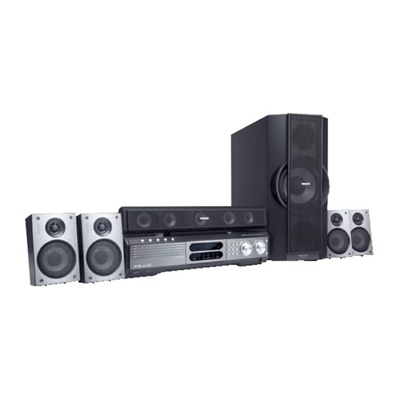
DVD Receiver
Service
Service
Service
Service
Service
Service Manual
©
Copyright 2003 Philips Consumer Electronics B.V. Eindhoven, The Netherlands
All rights reserved. No part of this publication may be reproduced, stored in a retrieval system or
transmitted, in any form or by any means, electronic, mechanical, photocopying, or otherwise
without the prior permission of Philips.
Published by KC 0311 Service Audio
Version 1.1
TABLE OF CONTENTS
Location of pc boards & Version variations ................ 1-2
Technical Specifications ............................................. 1-3
Measurement setup .................................................... 1-4
Service Aids, Safety Instruction, etc. ......................... 1-5
Disassembly Instructions & Service positions ........... 2-1
Service Test Programs ............................................... 3-1
Region codes setting, software upgrades, etc ........... 3-3
Set Block diagram .......................................................... 4
Set Wiring diagram ........................................................ 5
Front Board .................................................................... 6
ECO6 Tuner Board:
System Non-Cenelec ............ 7A
Power Module PWR207 ................................................ 8
AV Board ........................................................................ 9
5DTC Module ............................................................... 10
CD222 FE (Front End) Board ...................................... 11
CD222 BE (Back End) Board ...................................... 12
Set Mechanical Exploded view & parts list ................. 13
Revision List ................................................................ 14
Printed in The Netherlands
Subject to modification
MX3900D/
& MX3910D/
37
MX3950D/
& MX3960D/
37
Page
LASER PRODUCT
17
17
CLASS 1
GB
3139 785 30201
Advertisement
Chapters
Table of Contents


Need help?
Do you have a question about the MX3900D and is the answer not in the manual?
Questions and answers