Harman Kardon AVR125 Service Manual
Hide thumbs
Also See for AVR125:
- Owner's manual (44 pages) ,
- Brochure & specs (40 pages) ,
- Service manual (8 pages)
Table of Contents
Advertisement
harman/kardon
A/V DOLBY DIGITAL RECEIVER
SERVICE MANUAL
ESD WARNING......................................2
LEAKAGE TESTING.................................3
BASIC SPECIFICATIONS.........................4
FRONT PANEL CONTROLS.....................5
FRONT PANEL DISPLAY.........................7
REAR PANEL CONNECTIONS..................9
REMOTE CONTROL FUNCTIONS.............11
INSTALLATION AND CONNECTIONS........14
TROUBLESHOOTING GUIDE..................16
MICROPROCESSOR RESET...................16
UNIT EXPLODED VIEW..........................17
AVR125
CONTENTS
DISASSEMBLY PROCEDURE...............18
AMPLIFIER BIAS ADJUSTMENT............21
BLOCK DIAGRAM...............................22
IC PINOUTS.......................................23
TRANSISTOR PINOUTS.......................52
ELECTRICAL PARTS LIST....................53
PCB DRAWINGS................................62
SCHEMATICS....................................70
WIRING DIAGRAM..............................82
PACKAGING......................................83
harman/kardon, Inc.
250 Crossways Park Dr.
Woodbury, New York 11797
2/2005
Rev5
Advertisement
Table of Contents

Subscribe to Our Youtube Channel
Related Manuals for Harman Kardon AVR125


Summary of Contents for Harman Kardon AVR125
-
Page 1: Table Of Contents
AVR125 A/V DOLBY DIGITAL RECEIVER SERVICE MANUAL CONTENTS ESD WARNING………………………….…….2 DISASSEMBLY PROCEDURE..………….18 LEAKAGE TESTING………………..……..3 AMPLIFIER BIAS ADJUSTMENT……...…21 BASIC SPECIFICATIONS…………….….…..4 BLOCK DIAGRAM………………………….22 FRONT PANEL CONTROLS………………...5 IC PINOUTS……………………………..….23 FRONT PANEL DISPLAY…………………….7 TRANSISTOR PINOUTS………..…..…….52 REAR PANEL CONNECTIONS……..….……9 ELECTRICAL PARTS LIST………..…..….53 REMOTE CONTROL FUNCTIONS……..…..11 PCB DRAWINGS……………………..……62... -
Page 2: Esd Warning
AVR125 Some semiconductor (solid state) devices can be damaged easily by static electricity. Such components commonly are called Electrostatically Sensitive (ES) Devices. Examples of typical ES devices are integrated circuits and some field effect transistors and semiconductor "chip" components. -
Page 3: Leakage Testing
AVR125 SAFETY PRECAUTIONS The following check should be performed for the continued protection of the customer and service technician. LEAKAGE CURRENT CHECK Measure leakage current to a known earth ground (water pipe, conduit, etc.) by connecting a leakage current tester... -
Page 4: Basic Specifications
Height measurement includes feet and chassis. All features and specifications are subject to change without notice. Harman Kardon is a registered trademark, and Power for the Digital Revolution is a trademark, of Harman Kardon, Inc. * Manufactured under license from Dolby Laboratories. -
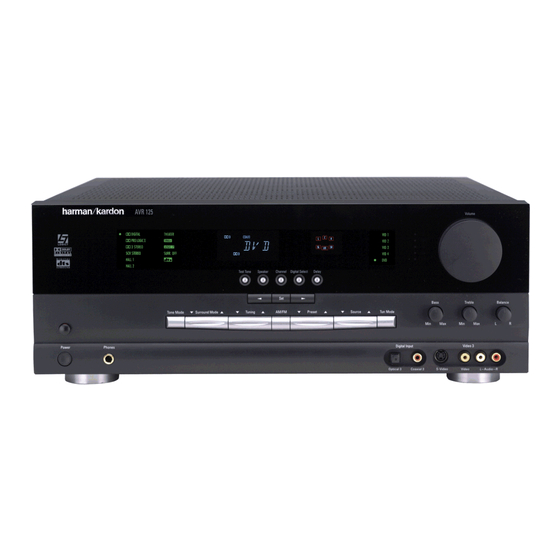
Page 5: Front Panel Controls
AVR125 FRONT-PANEL CONTROLS ı Û Ò Ô Ù Ú ˆ AVR 125 Ó AM/FM & 1 Main Power Switch ! Input Source Selector Ô Set Button 2 System Power Control @ Tuning Mode Selector Input Indicators 3 Power Indicator # Digital Optical 3 Input Ò... - Page 6 AVR125 FRONT-PANEL CONTROLS % Video 3 Video Input Jacks: These jacks may be In Manual tuning mode, tap the button lightly and note the receiver. (See pages 7–8 for a complete explana- that the tuner will step up one frequency increment per tion of the Information Display.)
-
Page 7: Front Panel Display
AVR125 FRONT-PANEL INFORMATION DISPLAY Q PO OPT 123 COAX 123 ANALOG AUTO TUNED ST PRESET SLEEP NIGHT PL II DSP VMAx NF LOGIC 7 CM F G H A Bitstream Indicators I Logic 7 Mode Indicators Q Tuned Indicator... - Page 8 AVR125 FRONT-PANEL INFORMATION DISPLAY remaining before the AVR 125 goes into the Standby mode. (See page 21 for more information.) O Memory Indicator: This indicator flashes when entering presets and other information into the tuner’s memory. P Stereo Indicator: This indicator lights when an FM station is being tuned in stereo.
-
Page 9: Rear Panel Connections
AVR125 REAR-PANEL CONNECTIONS ° fl › ‡ · fi ¡ ™ £ ¢ ∞ SURR SURR , 1A , 0.5A § ‹ ¶ • ª ‚ ⁄ ¤ ¡ AM Antenna › AC Power Cord h DVD Audio Inputs ™... - Page 10 AVR125 REAR-PANEL CONNECTIONS ¤ Switched AC Accessory Outlet: This outlet may Video 2 Video Inputs: Connect one of these be used to power any device you wish to have turned jacks to the PLAY/OUT composite or S-Video jacks on or off at the same time as the AVR 125. Any device on a TV, VCR or other video source.
-
Page 11: Remote Control Functions
AVR125 REMOTE CONTROL FUNCTIONS a Power Off Button b IR Transmitter Window c Program Indicator d Power On Button e Input Selectors POWER f AVR Selector g AM/FM Tuner Select h Test Button i Sleep Button TAPE j Surround Mode Selector... - Page 12 Digital Select sequence used to calibrate the AVR 125’s output levels. ate the AVR 125 and most recent Harman Kardon Button p to change the digital input) and then press (See pages 18–19 for more information on calibrating products.
- Page 13 AVR125 REMOTE CONTROL FUNCTIONS u Tuning Up/Down: When the tuner is in use, these AVR 125 when processing surround sound. After to operate another device or when a macro command pressing this button, the delay times are entered by...
-
Page 14: Installation And Connections
AVR125 INSTALLATION AND CONNECTIONS System Installation cable TV system. Note that if the antenna or connec- color to assist you in making the correct connections. After unpacking the unit, and placing it on a solid surface tion uses 300-ohm twin-lead cable, you must use the... - Page 15 AVR125 INSTALLATION AND CONNECTIONS should be connected to the Video 1 Out Jacks Power Connections on the AVR 125. This unit is equipped with two accessory AC outlets. They may be used to power accessory devices, but 2. Connect the analog audio and video outputs of a...
-
Page 16: Troubleshooting Guide
• Amplifier is in protection mode • Contact your local Harman Kardon service center, which you can due to internal problems locate by visiting our Web site at www.harmankardon.com No sound from surround or •... -
Page 17: Unit Exploded View
AVR125 AVR125 Exploded View 39-4 39-2 39-3 39-1 39-8 37-7 39-6 DESCRIPTION PARTS NO. Q,ty KNOB,VOLUME CBN1A155K128 WINDOW,FIP CGU1A280X KNOB,ROTARY CBN1A156K128 F.I.P (DISPLAY) BDAGE,HARMAN/KARDON KGB1A111Z SHEET KMZ1A077 # HFLCM2054C KMZ176 SHEET,FIP KMZ1A76 PANEL,FRONT CGW1A337R4YK128 BRACKET,SIDE CMD1A443 KNOB,FUNCTION CBT1A816M7G2 37-5... -
Page 18: Disassembly Procedure
AVR125 AVR125/225 DISASSEMBLY PROCEDURE <1> TOP-CABINET(21) REMOVAL 1. Remove 13 screws(S1,S7) and then remove the Top-cabinet. <2> FRONT PANEL ASS’Y REMOVAL 1. Remove the Top-cabinet, referring to the previous step<1>. 2. Disconnect the connect (BN72-Card canle)) on the FP PCB(37-1) from connector(CN72) on the Input PCB(39-1) 3. - Page 19 AVR125 <7>TUNER MODULE(40) REMOVAL 1. Remove the Top-cabinet, referring to the previous step<1>. 2. Disconnect the connector(CON1-Card cable) from connector(CN13) on the Input PCB ASS’Y(39-1). 3. Remove 2 screws(S8) and then remove the Tuner Module(40). <8>VIDEO PCB(39-2) REMOVAL 1. Remove the Top-cabinet, referring to the previous step<1>.
- Page 20 AVR125 DISASSEMBLY 1) REMOVAL OF TOP COVER 2) REMOVAL OF FRONT PANEL 3) PRINCIPAL PARTS LOACTION TUNER MODULE INPUT PCB TRANS FORMER MAIN PCB FRONT PCB...
-
Page 21: Amplifier Bias Adjustment
AVR125 AMPLIFIER SECTION BIAS ADJUSTMENT Measurement condition . No input signal or volume position is minimum. Standard value. ± . Ideal current = 48mA ( ± . Ideal DC Voltage = 21.12mV ( CUP11517X (MAIN PCB) CN63 CN61 CN62... - Page 22 AVR125...
-
Page 23: Block Diagram
AVR125 BLOCK DIAGRAM AVSS AVDD X'tal Clock Oscillator 8 to 3 Recovery Clock MCKO1 Generator MCKO2 Input Selector LRCK DAIF Audio BICK Decoder SDTO DAUX DVDD Error & CCLK Q-subcode DVSS AC-3/MPEG µP I/F STATUS CDTO buffer TVDD Detect... - Page 24 AVR125 DIR IC PIN ASSIGNMENT & BLOCK DIAGRAM PIN ASSIGNMENT (TOP VIEW) IPS0/RX4 INT0 OCKS0/CSN/CAD0 AVSS OCKS1/CCLK/SCL DIF0/RX5 TEST2 CM1/CDTI/SDA AK4114VQ CM0/CDTO/CAD1 DIF1/RX6 AVSS DIF2/RX7 Top View IPS1/IIC DAUX P/SN XTL0 MCKO2 XTL1 BICK SDTO...
- Page 25 AVR125 IC PIN FUNCTION AK4114VQ IC75 PIN/FUNCTION Pin Name Function IPS0 Input Channel Select 0 Pin in Parallel Mode Receiver Channel 4 Pin in Serial Mode (Internal biased pin) No Connect NC(AVSS) No internal bonding. This pin should be connected to AVSS.
- Page 26 AVR125 PIN/FUNCTION (Continued) Pin Name Function Power-Down Mode Pin When “L”, the AK4114 is powered-down and reset. Master Clock Operation Mode 0 Pin in Parallel Mode CDTO Control Data Output Pin in Serial Mode, IIC= “L”. CAD1 Chip Address 1 Pin in Serial Mode, IIC= “H”.
- Page 27 AVR125 D/A CONVERTER IC PIN ASSIGNMENT & BLOCK DIAGRAM PIN ASSIGNMENT (TOP VIEW) LOUT1- AVDD LOUT1+ VREFH DZFL2 DZFR2 DZFR1 DZFL3 AK4356VQ DZFL1 DZFR3 CAD0 DZFE CAD1 DIF2 Top View DIF1 BICK DIF0 MCLK CKS2 DVDD CKS1 n Block Diagram...
- Page 28 AVR125 D/A CONVERTER IC PIN FUNCTION (AK4356VQ) : IC78 PIN/FUNCTION Pin Name Function LOUT1- DAC1 Lch Negative Analog Output Pin LOUT1+ DAC1 Lch Positive Analog Output Pin DZFL2 DAC2 Lch Zero Input Detect Pin DZFR1 DAC1 Rch Zero Input Detect Pin...
- Page 29 AVR125 Pin Name Function DFS0 Double Speed Sampling Mode 0 Pin (Note) “L”: Normal Speed, “H”: Double Speed at DFS1 bit = “0”. CKS0 Input Clock Select 0 Pin (Note) CKS1 Input Clock Select 1 Pin (Note) CKS2 Input Clock Select 2 Pin...
-
Page 30: General Description
AVR125 November 1988 Revised November 1999 74ACT04SC : IC83, 84 74AC04 • 74ACT04 Hex Inverter General Description Features The AC/ACT04 contains six inverters. reduced by 50% on 74AC only Outputs source/sink 24 mA ACT04 has TTL-compatible inputs Ordering Code:... - Page 31 AVR125 AINR AINL VCOM View AGND SCLK MCLK LRCK SDTO DGND BLOCK DIAGRAM AGND DGND MCLK Clock Divider ∆Σ Decimation AINL Modulator Filter LRCK SCLK ∆Σ Decimation AINR Modulator Filter Serial I/O SDTO Interface VCOM Voltage Reference...
- Page 32 AVR125 A/D CONVERTER IC PIN FUNCTION (AK5380VT) : IC77 PIN/FUNCTION Pin Name Description AINR Rch Analog Input Pin AINL Lch Analog Input Pin NC Pin No internal bonding. VCOM Common Voltage Output Pin Normally connected to AGND with a 0.1µF ceramic capacitor in parallel with an electrolytic capacitor less than 2.2µF.
- Page 33 AVR125 PIN ASSIGNMENT (74HCU04AFN : IC71,72 ) LOGIC SYMBOL (10) (11) (13) (12) TRUTH TABLE...
- Page 34 Sheet 3/5 Ise Electronics Corporation :Display Pattern CM2054C Scale 3:1 Unit : mm 100.0 Color of illumination G:Green /(Blue Green) Rsh.O-N:Reddish Orange-N/(Red)
- Page 35 AVR125...
- Page 36 AVR125...
- Page 37 AVR125 AUDIO DSP (CS493263 - CLG : IC79) PIN No. Pin Name Function 1,12,23 +VD1 Digital Power supply. Normally +2.5v 2,13,24 DGND Digital Ground AUD3 SPDIF transmitter output/Digital audio output(N.C) Host write strobe pin(connected to GND with an external resistor)
-
Page 38: Top View
AVR125 PIN ASSIGNMENT.(CS493263) DGND1 MCLK AUDATA3, XMT958 SCLK WR,DS,EMWR,GPIO10 LRCLK RD,R/W,EMOE,GPIO11 AUDATA0 A1,SCDIN AUDATA1 A0,SCCLK AUDATA2 6 5 4 3 2 1 44 43 42 41 40 DATA7,EMAD7,GPIO7 DATA6,EMAD6,GPIO6 DATA5,EMAD5,GPIO5 RESET DATA4,EMAD4,GPIO4 AGND CS493XXX-CLG 44-pin PLCC Top View DGND2... - Page 39 AVR125 TC9162AF (FUNCTION/INPUT : IC30) TC9162AF (FUNCTION/INPUT : IC30) BLOCK DIAGRAM BLOCK DIAGRAM L-COM L-COM R-COM R-COM L-COM L-COM R-COM R-COM L-COM L-COM R-COM R-COM L-COM L-COM R-COM R-COM DATA DATA SHIFT REGISTER SHIFT REGISTER PIN ASSIGNMENT (TOP VIEW) Top view No.
- Page 40 AVR125 BLOCK DIAGRAM VFD DRIVER IC PIN FUNCTION (LC75725E) : IC74 Pin No. Function Handling when unused 1, 13 Driver block power supply connection. (Both pins must be connected.) — — Logic block power supply connection. Provide a voltage between 4.5 and 5.5 V.
- Page 41 AVR125 BLOCK DIAGRAM Clock control X0, X1 RSTX circuit X0, X1A core MC-16LX family Interrupt controller PPG0, 1 PPG2, 3 8-/16-bit PPG PPG4, 5 AIN0, 1 BIN0, 1 8-/16-bits UD counter Communication prescaler ZIN0, 1 EXTC SIN0 µPG MT00...
- Page 42 AVR125 M-COM IC PIN ASSIGNMENT & BLOCK DIAGRAM PIN ASSIGNMENT (TOP VIEW) P 20/A16 P 21/A17 P22/A18 P57/CLK P23/A19 RSTX P24/A20/PPG0 P56/RDY P 25/A21/PPG1 P55/HAKX P26/A22/PPG2 P54/HRQ P27 /A23/PPG3 P53/WRHX P30 /A00/AIN0 P52/WRLX P 31/A01/BIN0 P51/RDX P50/ALE P32/A02/ZIN0 PA3/OUT3...
- Page 43 AVR125 IC PIN FUNCTION (M-COM : MB90F476APFG) : IC72 LQFP Pin Name Circuit Type Function Oscillator pin Oscillator pin 32 kMHz Oscillator pin 32 kMHz Oscillator pin RSTX Reset input pin General-purpose I/O ports P00 to P07 A pull-up resistor can be attached using the pull-up resistor setting register (RDR0) (RD07 to RD00 = 1).
- Page 44 AVR125 LQFP Pin Name Circuit Type Function General-purpose I/O ports In the external bus mode, the pin functions as an external address pin. (CMOS/H) AIN0 The pin is an 8-/16-bit up-and-down timer input pin (ch0). General-purpose I/O port In the external bus mode, the pin functions as an external address pin.
- Page 45 AVR125 LQFP Pin Name Circuit Type Function General-purpose I/O port In the external bus mode, the pin functions as ALE pin. (CMOS) In the external bus mode, the pin functions as an address capture enable signal (ALE) pin. General-purpose I/O port In the external bus mode, the pin functions as the RDX pin.
- Page 46 AVR125 LQFP Pin Name Circuit Type Function General-purpose I/O port SOT0 (CMOS) The pin functions as an UART data output pin. General-purpose I/O port SCK0 (CMOS/H) The pin functions as an UART clock I/O pin. General-purpose I/O port TIN0 (CMOS/H) The pin functions as the event input pin of the 16-bit reload timer.
- Page 47 AVR125 NJM2068M : IC23~29 , 32~34 , 82,88...
- Page 48 AVR125 BLOCK DIAGAM (NJM2296M ) : IC41, 43, 44 Vin1 Vin2 Vout1 6.2dB dirver Vin3 6.2dB Vout2 dirver Vin4 Vout3 6.2dB dirver Vin5...
- Page 49 AVR125 NJM4556AM : IC86...
- Page 50 AVR125 TC9164AF (FUNCTION/INPUT) : IC22 BLOCK DIAGRAM L-COM R-COM L-COM R-COM L-COM R-COM DATA SHIFT REGISTER TC9163AF (FUNCTION/INPUT) : IC20 BLOCK DIAGRAM L-COM R-COM L-COM R-COM L-COM R-COM DATA SHIFT REGISTER...
- Page 51 AVR125 TC9482F (ELECTRONIC VOLUME/INPUT) : IC31 TEST L-OUTA L-OUTA L-INA L-INA latch L-A-GNDA L-A-GNDA latch L-OUTB L-OUTB 3 to 7 L-INB L-INB decoder Same as L-ch latch Circuit L-A-GNDB 4 to 13 L-A-GNDB latch decoder L-OUTC L-OUTC L-INC 10...
-
Page 52: Transistor Pinouts
AVR125 TRANSISTOR, REGULATOR IC BLOCK DIAGRAM TO-92L TO-92M TO-92 TO-220 1. Emitter 1. Emitter 1. Emitter 1. GND 2. Collector 2. Collector 2. Collector 2. INPUT 3. Base 3. Base 3. Base 3. OUTPUT 1 2 3 1 2 3... -
Page 53: Electrical Parts List
AVR125 AVR125 ELECTRICAL PARTS LIST Reference Designator Part Number Description PCB , FRONT Capacitors C703 HCBS1H821KBT CAP , CERAMIC 820PF 50V K C704,735,773,774,777,778,864 HCEA1VH100T CAP , ELECT 10UF 35V C712 HCEA1HH1R0T CAP , ELECT 1UF 50V C713,730,732,736,770,771,805, HCBS1H223ZFT CAP , CERAMIC 0.022UF 50V Z... - Page 54 AVR125 Reference Designator Part Number Description Intergrated Circuits IC72 BVIMB90F476APFG IC , FLASH U-COM FUJITSU IC73 HRVRPM6938H4 SENSOR , REMOTE RPM6938-H4 IC74 HVILC75725E IC , VFL DRIVER LC75725E IC80 HVITC9215AF TC9215AF IC81,82,88 HVINJM2068MTE1 I.C , OP AMP NJM2068M-TE1 IC83,84 HVI74ACT04SC I.C , HEX INVERTER...
- Page 55 AVR125 Reference Designator Part Number Description BN41 CWZAVR125BN41 WIRE ASS'Y (SHIELD) BN80 CWB2B908320EW WIRE ASS'Y BN81 CWB2B906250BM WIRE ASS'Y BN83 CWB1C902250BM WIRE ASS'Y BN84 CWB2B905100EN WIRE ASS'Y BN85,90 CWB2B902090EN WIRE ASS'Y BN87 CWZAVR2550BN87 WIRE ASS'Y (SHIELD) BN88 CWB2B904070EN WIRE ASS'Y...
- Page 56 AVR125 Reference Designator Part Number Description C904 KCKDKS472ME CAP , CERAMIC(X1/Y2/SC) 0.0047UF/2.5KV C906 HCEA1EH102E CAP , ELECT 1000UF 25V C915,916 HCET63VFHS123ND CAP , ELECT 12000UF 63V C917 HCEA1EH332E CAP , ELECT 3300UF 25V C918 HCEA1EH222E CAP , ELECT 2200UF 25V...
- Page 57 AVR125 Reference Designator Part Number Description R671~675 CRD20TJ911T RES , CARBON 910 OHM 1/5W J R676,677 CRD25TJ182T RES , CARBON 1.8K OHM 1/4W J R681~685,960,992 CRD20TJ562T RES , CARBON 5.6K OHM 1/5W J R686~690,930,932,966,998 CRD20TJ103T RES , CARBON 10K OHM 1/5W J...
- Page 58 AVR125 Reference Designator Part Number Description C297~302,323,324,327,328,334,347, 348,358,420,430,439,446,449,460, HCBS1H223ZFT CAP , CERAMIC 0.022UF 50V Z 730,766 C303~308 HCEA1HH220T CAP , ELECT 22UF 50V C336,357,461,735,921 CCKT1H223ZF CAP , CERAMIC 0.022UF 50V ZF C339,340,772 HCBS1H103ZFT CAP , CERAMIC 0.01UF 50V Z...
- Page 59 AVR125 Reference Designator Part Number Description Q302,902 HVTKRA107MT KRA107M Q395,396 HVTKTC2874BT T.R , MUTE KTC2874B Q701,702 HVTKSC2316YT KSC2316Y Q901,903 HVTKTA1271YT KTA1271Y Q904 HVTKRC107MT KRC107M Q455 HVTKSA614Y KSA614Y Intergrated Circuits IC20 HVITC9163AF I.C , FUNCTION TC9163AF IC21,23~29,32~34 HVINJM2068MTE1 I.C , OP AMP...
- Page 60 AVR125 Reference Designator Part Number Description R419,425,431,436,437,453,454,456,457, CRD20TJ750T RES , CARBON 75 OHM 1/5W J 464,467,470,471,473,474,705~707,709 R422,455,459,702,703,710,711,722,724, CRD20TJ1R0T RES , CARBON 1 OHM 1/5W J 736,774,775 R433,466,469,906 CRD20TJ100T RES , CARBON 10 OHM 1/5W J R725 CRD20TJ183T RES , CARBON...
- Page 61 AVR125 Reference Designator Part Number Description CB72 CWC1B2A32A210B CABLE , CARD CHASSIS MISCELLANEOUS T901 CLT5V030ZU TRANS , POWER TUNER MODULE CNVKSTM9014MS07 TUNER MODULE KSTM9014MS07 CLZ9W003Z FERRITE , RING...
-
Page 62: Pcb Drawings
AVR125... - Page 63 AVR125...
- Page 64 AVR125...
- Page 66 AVR125...
- Page 67 AVR125...
- Page 69 AVR125...
-
Page 83: Packaging
AVR125 AVR125 1. Instruction manual ass'y - Accessories 2. Package Drawing TAPE OPP TAPE OPP MANUAL ASS'Y FM 1 POLE ANT(UL) POLY BAG MANUAL INSTRUCTION SNOW PAD (L) SNOW PAD (R) REMOCON TRANSMITTER ASS'Y BATTERY ASS'Y AM LOOP ANTENNA ASS'Y...
Need help?
Do you have a question about the AVR125 and is the answer not in the manual?
Questions and answers