Table of Contents
Advertisement
SERVICE MANUAL
Main Section
I Specifications
I Preparation for Servicing
I Adjustment Procedures
I Schematic Diagrams
I CBA's
I Exploded views
I Parts List
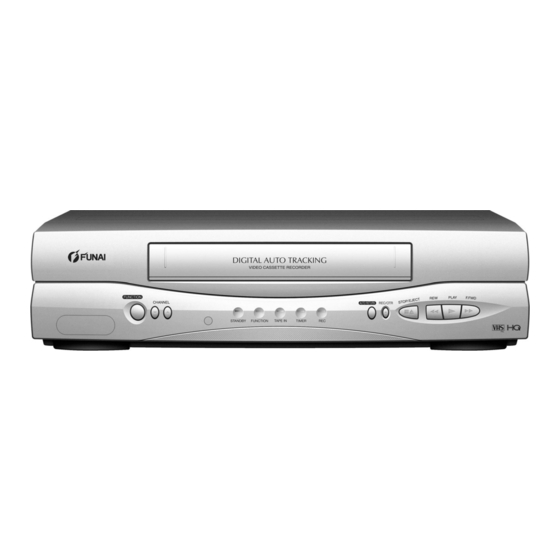
VIDEO CASSETTE RECORDER
31A-250/31D-250
31C-250
When servicing the deck
mechanism, refer to MK14 Deck
Mechanism Section.
Deck Mechanism Part No.:
31A-250/31D-250: N25A0FL
31C-250: N25A1FL
PAL
PAL
SECAM
Advertisement
Table of Contents


Need help?
Do you have a question about the 31A-250 and is the answer not in the manual?
Questions and answers