Table of Contents
Advertisement
Quick Links
This document is printed on chlorine free (ECF) paper with soy ink.
SY 011548
20010301-59800
SERVICE MANUAL
CONTENTS
SPECIFICATIONS .............................................................................. 3
PANEL LAYOUT .................................................................................. 4
CIRCUIT BOARD LAYOUT ................................................................. 6
WIRING ............................................................................................... 6
BLOCK DIAGRAM .............................................................................. 7
DISASSEMBLY PROCEDURE ........................................................... 8
LSI PIN DISCRIPTION ....................................................................... 11
IC BLOCK DIAGRAM ........................................................................ 15
DIMENSIONS ................................................................................... 17
CIRCUIT BOARDS ........................................................................... 18
TEST PROGRAM & INITIALIZE ....................................................... 28
MIDI IMPLEMENTATION CHART ..................................................... 40
PARTS LIST
OVERALL CIRCUIT DIAGRAM
HAMAMATSU, JAPAN
1.494K-059 Y.K
Printed in Japan '01, 02
Advertisement
Table of Contents

Related Manuals for Yamaha an200


Summary of Contents for Yamaha an200
- Page 1 SERVICE MANUAL CONTENTS SPECIFICATIONS ................3 PANEL LAYOUT .................. 4 CIRCUIT BOARD LAYOUT ..............6 WIRING ....................6 BLOCK DIAGRAM ................7 DISASSEMBLY PROCEDURE ............8 LSI PIN DISCRIPTION ............... 11 IC BLOCK DIAGRAM ................ 15 DIMENSIONS ................... 17 CIRCUIT BOARDS ................18 TEST PROGRAM &...
- Page 2 IMPORTANT NOTICE This manual has been provided for the use of authorized Yamaha Retailers and their service personnel. It has been assumed that basic service procedures inherent to the industry, and more specifically Yamaha Products, are already known and understood by the users, and have therefore not been restated.
-
Page 3: Specifications
338.0 (W) x 208.9 (D) x 51.7 (H) mm, 1600 g 10.ACCESSORIES CD ROM (for Windows and Macintosh) Owner's Manual AC Adaptor (Power supply recommendation may vary from country to country. Please check with your nearest Yamaha dealer for further details.) -
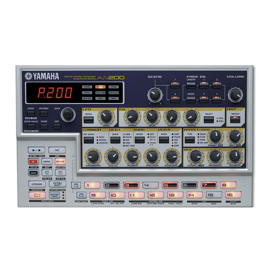
Page 4: Panel Layout
AN200 PANEL LAYOUT Top Panel Main block Voice block Control block Keyboard block Main Block [SONG] button [PATTERN] button [DATA] knob [SHOW VALUE] button [STORE] button [EXIT] button VOICE BLOCK [SCENE] group [SCENE] knob [1] button [2] button [FREE EG] group... - Page 5 AN200 [RELEASE] knob [SELECT] button [DIST] group [SWITCH] button [COMMON] group [KEY ASGN] button [VCO1] group [WAVE] button [SYNC] group [MODE] button [VCO 2] group [WAVE] button [PORTAMENTO] knob [VCO 1/2] knob [FM DEPTH] knob [SYNC PITCH] knob [NOISE LEVEL] knob...
-
Page 6: Circuit Board Layout
AN200 I CIRCUIT BOARD LAYOUT PLG150-AN I WIRING CN2(7P) CN5(15P) CN6(4P) CN4(6P) CN3(15P) CN1(15P) CN4(6P) CN2(15P) CN3(4P) 28C99-8818208 LOCATION DESTINATION CONNECTOR NAME PIN/LENGTH 16P / L=80 LED-CN1 PN-CN1 KR-KR 7P / L=450 DM-CN2 PN-CN5 4P / L=380 DS-KR PN-CN3 DM-CN6... - Page 7 SWING REVERS << >> PATTERN KEYBOARD SELECT STEP STEP TRACK TRACK 9~16...
-
Page 8: Disassembly Procedure
AN200 DISASSEMBLY PROCEDURE [180] AN200 Bottom side Bottom Assembly Wooden bolster (Fig. 1) (Fig. 1-1) [185] [180]: Bind Head Tapping Screw-B 3.0X6 MFZN2Y (EP600130) [185]: Bind Head Tapping Screw-B 3.0X6 MFZN2Y (EP600130) Bottom Assembly (time required: about 1 min) Remove the five (5) screws marked [180] and the two (2) screws marked [185]. - Page 9 AN200 DM Circuit Board (time required: about 2 min) Remove the bottom assembly. (See Procedure 1.) Remove the PLG150-AN circuit Board. (See Procedure 2.) Remove the six (6) screws marked [120]. The DM circuit board can then be removed. (Fig. 2)
- Page 10 AN200 [40] (Fig. 5) [40]: Bind Head Tapping Screw-P 2.6X8 MFZN2Y (EP620100) LED Circuit Board (time required: about 5 min) Remove the bottom assembly. (See Procedure 1.) Remove the PLG150-AN circuit Board. (See Procedure 2.) Remove the DM circuit Board. (See Procedure 3.) Remove the PN circuit Board.
- Page 11 AN200 LSI PIN DISCRIPTION HG73C205AFD (XU947C00) SWX00B TONE GENERATOR DM: IC17 NAME FUNCTION NAME FUNCTION Initial clear CMA3 RFCLKI PLL Clock CMA8 Program address bus PLL Control CMA2 AVDD_PLL Power supply read signal AVSS_PLL Ground CMA1 Program address bus MODE0...
- Page 12 AN200 YSS236-F (XT013A00) VOP3 PLG150-AN: IC4 NAME FUNCTION NAME FUNCTION Power supply WA17 Serial output WA16 WA15 Ground WA14 Power supply External memory address bus WA13 WA12 WA11 Serial output WA10 Ground Power supply WDCK Data enable for DAC WA09...
- Page 13 AN200 HD6413002FP16 (XQ375A00) CPU PLG150-AN: IC1 NAME FUNCTION NAME FUNCTION Port A Address bus Power supply Address bus Port B Ground PB6//DREQ0 P60//WAIT PB7//DREQ1 P61//BREQ Port 6 P62//BACK /RESO Reset Ground Oout P90/TXD0 Transmit data (MIDI OUT) /STBY Stand-by mode signal...
- Page 14 AN200 UPD63200GS-E1 (XP867A00) DAC (Digital to Analog Converter) DM: IC16 NAME FUNCTION NAME FUNCTION 4/8F 4/8 Fs selection R. REF Channel R voltage reference L. REF Channel L voltage reference D. GND Digital ground 16 BIT 16 bit/18 bit selection L.
-
Page 15: Block Diagram
AN200 IC BLOCK DIAGRAM SN74HC157NSR (XW110A00) MM74HC74ASJX (XY153A00) MM74HC157SJX(XY310A00) HD744C74FPEL (XL096A00) Quad 2 to 1 Multiplexer (XW890A00) TC74HC74AF EL Dual D-Type Flip-Flop DM: IC7 DM: IC14 SELECT IC25 STROBE 1CLR 2CLR INPUTS OUTPUTS TC74HC245AF (XS720A00) HD74HC273FP XU533A00 HD74HC4051FPEL (XP373A00) HD74HC245FPV (XV611A00) - Page 16 AN200 (XQ781A00) (XR294A00) TC74HCT04AF-T1 (XI297A00) NJM4580E-T1 NJM3414AM-T1 Hex Inverter Dual Operational Amplifier Dual Operational Amplifier DM: IC4 DM: IC11 PN: IC9 +DC Voltage +DC Voltage Output A Output A Supply Supply Inverting Inverting Output B Output B Input A Input A...
-
Page 17: Dimensions
AN200 DIMENSIONS 51.7 mm (H) SONG PATTERN STORE PITCH GATE TIME VELOCITY INST SEL BEAT 338 mm (W) -
Page 18: Circuit Boards
AN200 CIRSUIT BOARDS DM CIRCUIT BOARD OUTPUT STAND BY MIDI PHONES DC IN L/MONO to PLG150-AN CN1 to PN CN3 to PN CN5 Battery VN103500 VN103600 (Battery holder for VN103500) Battery Notice for back-up battery removal push the battery as shown in figure, then the battery will pop up. - Page 19 AN200 MIDI to PN CN3 to PN CN4 to PN CN2 Component side to PN CN6 2NA-V625760 2 Note: See parts list for details of circuit board component parts.
- Page 20 AN200 DM CIRCUIT BOARD...
- Page 21 AN200 Pattern side 2NA-V625760 2...
- Page 22 AN200 DM CIRCUIT BOARD PN CIRCUIT BOARD to DM CN6 to DM CN3 to DM CN4 DATA SPEED ATTACK SONG PATTERN DETAIL SHCW STORE EXIT VALUE POLY PULSE MONO UNISON VARI KEYASGN MLTSAW MODE WAVE PORTAMENTO VCO 1/2 FM DEPTH...
- Page 23 AN200 to DM CN4 LENGTH VOLUME SCENE MODE DECAY SUSTAIN RELEASE ATTACK SELECT SWITH PARAM/ WET/ DECAY WAVE VCO1 FLGR PULSE RFSR TYPE VCO2 OD+AMP SINE MODE FM DEPTH SYNC PITCH NOISE LEVEL CUTOFF/ RESONANCE FEG DEPTH TYPE Component side 2NA-V488620 Note: See parts list for details of circuit board component parts.
- Page 24 AN200 PN CIRCUIT BOARD...
- Page 25 AN200 Pattern side 2NA-V488620 Note: See parts list for details of circuit board component parts.
- Page 26 AN200 PLG150-AN Circut Board to DM CN5 N.C. Component side Pattern side 2NA-V414740 Note: See parts list for details of circuit board component parts.
- Page 27 AN200 LED CIRCUIT BOARD Component side SONG PATTERN STORE PIT CH GATE TIME VELOCITY INST SEL BEAT Note: See parts list for details of circuit board component parts. 2NA-V488650...
-
Page 28: Test Program & Initialize
AN200 TEST PROGRAM & INITIALIZE 1. TEST PROGRAM PREPERATIONS Following measuring instruments and jigs are required for the test. Measuring instruments : frequency counter(input impedance: more than 1M Ω) oscilloscope(input impedance: more than 1M Ω) volt meter(JIS-C curve, input impedance: more than 1M Ω, 0 dBm: 1mW 600 Ω) distortion meter(input impedance: more than 1M Ω) - Page 29 AN200 The test program Test No. Test Item Test Conditions, Judgment Criteria, etc OK/NG RAM BATTERY OK/NG SW & LED OK/NG LED visually check the lights DATA ENTRY OK/NG (0-23-0) KNOB OK/NG (255,254-127-1, 0) MIDI OK/NG WAVE ROM OK/NG OUTPUT(L) +3.0 +/- 2dBm load 10k Ω...
- Page 30 AN200 C-3 SW & LED Display of Test Results Press the panel switches according to the order indicated by the LCD and confirm that all switches are working properly. Confirm that the LED corresponding to the panel switch lights on.
- Page 31 AN200 -4.0 +/- 2 dBm (load 33 Ω) ADistortion: less than C-6 MIDI PHONES-L: 0.6% less than -60dBm(load 33 Ω) PHONES-R: Display of Test Results Not appearing After connecting the MIDI IN to the MIDI OUT via a MIDI cable, Test End execute the test.
- Page 32 AN200 C-11 PB RAM Display of Test Results Not appearing Test End Rotate [DATA ENTRY] knob clockwise to proceed to the next test. Check RAM of the plug-in board which is built in the unit. C-14 FACTORY SET Display of Test Results This test is used to initialize the data to the factory settings.
-
Page 33: Error Messages
This appears when the voltage of the internal backup battery becomes Err1 Err1 Err1 Err1 Err1 Battery Low low. Have the battery replaced by your local Yamaha dealer or any (flashes) Yamaha-authorized service personnel. This appears when too much MIDI data has been received at one time, Err2 Err2 Err2... - Page 34 AN200...
- Page 35 AN200...
- Page 36 AN200...
- Page 37 AN200...
- Page 38 AN200...
- Page 39 AN200...
-
Page 40: Midi Implementation Chart
AN200 I MIDI IMPLEMENTATION CHART YAMAHA [ DESKTOP CONTROL SYNTHESIZER ] Date:20-DEC-2000 Model AN200 MIDI Implementation Chart Version : 1.0 Transmitted Recognized Remarks Function... Basic Default 1 - 4 1 - 4 Channel Changed 1 - 16 1 - 16... -
Page 41: Parts List
AN200 PARTS LIST CONTENTS OVERALL ASSEMBLY .................. 2 PN ASSEMBLY ..................... 4 ELECTRICAL PARTS ................... 5 Note) DESTINATION ABBREVIATIONS Australian model South African model British model Chinese model Canadian model South-east Asia model German model Taiwan model European model U.S.A. model... - Page 42 AN200 OVERALL ASSEMBLY Upper Case Assembly PN Assembly See page 4. Bottom Assembly 170b 170a...
- Page 43 AN200 PART NO. DESCRIPTION REMARKS QTY RANK REF NO. Overall Assembly AN200 JUEW (V678970) V 6 9 5 3 1 0 0 Upper Case Assembly Upper Case (V667890) V 6 5 5 3 6 0 0 Protector Adhesive Tape #500 8mm...
- Page 44 AN200 PN ASSEMBLY PART NO. DESCRIPTION REMARKS QTY RANK REF NO. PN ASSEMBLY AN200 PN Assembly (V679220) V 4 8 8 6 2 0 0 Circuit Board V 4 1 6 2 6 0 0 Button LENGHT, MODE, DETAIL, KEY ASGN, WAVE, MODE,...
- Page 45 AN200 ELECTRICAL PARTS DESCRIPTION REMARKS PART NO. QTY RANK REF NO. ELECTRICAL PARTS AN200 V 6 2 5 7 6 0 0 Circuit Board DM J (XZ156D0) V 4 8 8 6 4 0 0 Circuit Board LED J (XZ192D0)
- Page 46 AN200 DESCRIPTION REMARKS PART NO. QTY RANK REF NO. US061270 27P 50V J Ceramic Capacitor-CH(chip) US063100 1000P 50V K Ceramic Capacitor-B (chip) US063220 2200P 50V K Ceramic Capacitor-B (chip) US135100 Ceramic Capacitor-F (chip) 0.1000 16V Z UF037100 Electrolytic Cap. (chip)
- Page 47 AN200 DESCRIPTION REMARKS PART NO. QTY RANK REF NO. V 6 1 9 6 6 0 0 EMI Filter (chip) NFM4516P13C204FT1 VR193800 LC Filter STF-104ZB-TBM V 6 1 9 6 6 0 0 EMI Filter (chip) NFM4516P13C204FT1 V 6 1 9 6 6 0 0...
- Page 48 AN200 DESCRIPTION REMARKS PART NO. QTY RANK REF NO. VR579900 Chip Inductance BK2125HS601-T VR579900 Chip Inductance BK2125HS601-T VR579900 Chip Inductance BK2125HS601-T VR579900 Chip Inductance BK2125HS601-T VR579900 Chip Inductance BK2125HS601-T VR579900 Chip Inductance BK2125HS601-T VR579900 Chip Inductance BK2125HS601-T VR579900 Chip Inductance...
- Page 49 AN200 DESCRIPTION REMARKS PART NO. QTY RANK REF NO. RD355100 Carbon Resistor (chip) 100 63M J RD350000 Carbon Resistor (chip) 0 63M J RD350000 Carbon Resistor (chip) 0 63M J RD355100 Carbon Resistor (chip) 100 63M J RD355100 Carbon Resistor (chip)
- Page 50 AN200 DESCRIPTION REMARKS PART NO. QTY RANK REF NO. R106 RD358100 100K 63M J Carbon Resistor (chip) R107 RD358100 100K 63M J Carbon Resistor (chip) RD357220 R108 22K 63M J Carbon Resistor (chip) RD357220 R109 Carbon Resistor (chip) 22K 63M J...
- Page 51 AN200 DESCRIPTION REMARKS PART NO. QTY RANK REF NO. US064100 0.0100 50V K Ceramic Capacitor-B (chip) US064100 0.0100 50V K Ceramic Capacitor-B (chip) US064100 0.0100 50V K Ceramic Capacitor-B (chip) US064100 Ceramic Capacitor-B (chip) 0.0100 50V K US064100 Ceramic Capacitor-B (chip) 0.0100 50V K...
- Page 52 AN200 DESCRIPTION REMARKS PART NO. QTY RANK REF NO. XU533A00 HD74HC273FP D-FF XY198A00 MM74HC273SJX D-FF XU533A00 HD74HC273FP D-FF XY198A00 MM74HC273SJX D-FF XU533A00 HD74HC273FP D-FF XY198A00 MM74HC273SJX D-FF XP373A00 HD74HC4051FPEL MULTIPLEXER XY549A00 TC74HC4051AFEL MULTIPLEXER XP373A00 HD74HC4051FPEL MULTIPLEXER XY549A00 TC74HC4051AFEL MULTIPLEXER XR294A00...
- Page 53 AN200 DESCRIPTION REMARKS PART NO. QTY RANK REF NO. VU067800 LD61 SEL6210S-TP5 RED VU067800 LD62 SEL6210S-TP5 RED SWITCH RE047470 47KX4 Resistor Array RE047220 Resistor Array 22KX4 RE047470 Resistor Array 47KX4 RE047220 Resistor Array 22KX4 RE047220 Resistor Array 22KX4 RE047220 22KX4...
- Page 54 AN200 DESCRIPTION REMARKS PART NO. QTY RANK REF NO. V 0 0 7 5 9 0 0 B 10.0K RK11K1130 FM DEPTH Rotary Variable Resistor V 0 0 7 5 9 0 0 B 10.0K RK11K1130 ATTACK Rotary Variable Resistor V 0 0 7 5 9 0 0 B 10.0K RK11K1130...
- Page 55 AN200 DESCRIPTION REMARKS PART NO. QTY RANK REF NO. XV839A00 SDM4260CLU-6S DRAM 4M XV077A00 MSM514260C-60JS DRAM 4M XV839A00 SDM4260CLU-6S DRAM 4M XV894A00 TC74VHC153FT MULTIPLEXER XV890A00 TC74VHC14FT INVERTER XW711A00 HD74LV14AT INVERTER XU797A00 IC13 TC74VHC245FT BUFFER XW744A00 BUFFER IC13 HD74LV245AT XV893A00 TC74VHC139FT...
- Page 56 AN200 AN200 OVERALL CIRCUIT DIAGRAM 1/3 (DM) to PN CN2 to PN CN4 to PN CN5 OP AMP PHONES OUTPUT L / MONO REGURATOR +5V TRANSCEIVER OUTPUT R MULTIPLEXER OP AMP OP AMP OP AMP INVERTER INVERTER INVERTER REGURATOR +3.3V...
- Page 57 AN200 AN200 OVERALL CIRCUIT DIAGRAM 2/3 (PN, LED) to DM CN3 to DM CN4 to DM CN6 to DM CN2 D-FF TIPLEXER D-FF TRANSCEIVER TIPLEXER OP AMP D-FF D-FF D-FF PN: 28CCI-8818206 Note: See parts list for details of circuit board component parts.