Sony RDR-HX520 Service Manual
Hide thumbs
Also See for RDR-HX520:
- Operating instructions manual (116 pages) ,
- Service manual (105 pages) ,
- Service manual (105 pages)
Table of Contents
Advertisement
Quick Links
SERVICE MANUAL
for RDR-HX520/HX720/HX722/
HX725/HX727/HX920/HX925
for RDR-HX525/HX725
for RDR-HX525/HX725/HX727/HX925
System
Laser: Semiconductor laser
Channel coverage:
PAL (B/G, D/K, I)
VHF: E2 to E12, R1 to R12, Italian A
to H, Ireland A to J, South Africa 4 to
13
UHF: E21 to E69, R21 to R69, B21 to
B69
CATV: S01 to S05, S1 to S20
HYPER: S21 to S41
SECAM (L) (for French RDR-HX520/
HX725/HX727/HX920 and RDR-
HX925 models only)
VHF: F2 to F10
UHF: F21 to F69
CATV: France B to Q
HYPER: S21 to S41
The above channel coverage merely ensures
the channel reception within these ranges. It
does not guarantee the ability to receive
signals in all circumstances. For details, see
"Receivable channels"
Video reception: Frequency synthesizer
system
Audio reception: Split carrier system
Aerial out: 75-ohm asymmetrical aerial
socket
Timer: Clock: Quartz locked/Timer
indication: 24-hour cycle (digital)/Power
back-up duration: 1 hour
Video recording format: MPEG-2,
MPEG-1
Audio recording format/applicable bit
rate: Dolby Digital 2 ch
256 kbps/128 kbps (in EP and SLP
mode)
RDR-HX520/HX525/HX720/HX722/
HX725/HX727/HX920/HX925
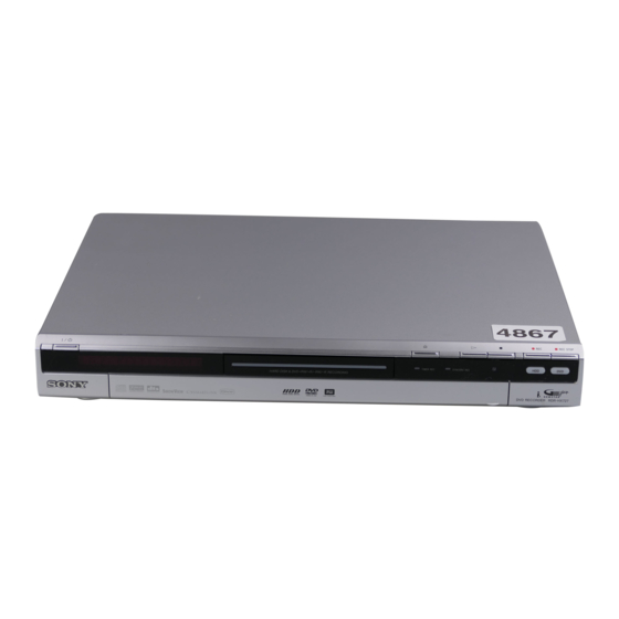
Photo: RDR-HX525
SPECIFICATIONS
Inputs and outputs
LINE 2 OUT
(
AUDIO
): Phono jack/2 Vrms/10 kilohms
(
VIDEO
): Phono jack/1.0 Vp-p
S VIDEO
(
): 4-pin mini DIN/Y: 1.0 Vp-p,
C: 0.3 Vp-p (PAL)
LINE 2 IN
(
AUDIO
): Phono jack/2 Vrms/more than
22 kilohms
VIDEO
(
): Phono jack/1.0 Vp-p
S VIDEO
(
): 4-pin mini DIN/Y: 1.0 Vp-p,
C: 0.3 Vp-p (PAL)
LINE 1 – TV: 21-pin
CVBS IN/OUT
S-Video/RGB OUT (upstream)
LINE 3/DECODER
CVBS IN/OUT
S-Video/RGB IN
(RGB signal cannot be recorded, except
with French RDR-HX520/HX725/HX727/
HX920 and RDR-HX925 models.)
S-Video OUT (downstream)
Decoder
DV IN
: 4-pin/i.LINK S100
DIGITAL OUT
0.5 Vp-p/75 ohms
COMPONENT VIDEO OUT
(Y, P
/C
, P
B
B
Phono jack/Y: 1.0 Vp-p, P
P
/C
: 0.7 Vp-p
R
R
G-LINK: mini jack
(for French RDR-HX525/HX725/HX727
and RDR-HX725 models only)
General
Power requirements: 220-240 V AC, 50/
60 Hz
Power consumption:
RDR-HX520/HX525: 42 W
RDR-HX720/HX722/HX725/HX727/
HX920/HX925: 44 W
Dimensions (approx.):
430 × 65 × 328 mm (width/height/
depth) incl. projecting parts
Hard disk drive capacity:
RDR-HX520/HX525: 80 GB
RDR-HX720/HX722/HX725/
HX727: 160 GB
RDR-HX920/HX925: 250 GB
: 21-pin
Mass (approx.): 4.2 kg
Operating temperature: 5ºC to 35ºC
Operating humidity: 25% to 80%
Supplied accessories:
Mains lead (1)
Aerial cable (1)
Re
Set top box controller (1)
(
COAXIAL
): Phono jack/
(for French RDR-HX525/HX725/
HX727/HX925 models only)
R6 (size AA) batteries (2)
/C
):
R
R
Specifications and design are subject to
/C
: 0.7 Vp-p,
B
B
change without notice.
Compatible colour systems
This recorder is designed to record using the
PAL colour system and play back using the
PAL or NTSC colour systems.
For French RDR-HX520/HX725/HX727/
HX920 and RDR-HX925 models only
The signals of the SECAM colour system can
be received or recorded but played back in the
PAL colour system only. Recording of video
sources based on other colour systems cannot
be guaranteed.
RMT-D230P/D231P
AEP Model
RDR-HX520/HX720/HX722/HX725/
HX727/HX920/HX925
UK Model
RDR-HX520/HX525/
HX720/HX725
mote commander (remote) (1)
DVD RECORDER
Advertisement
Table of Contents

Related Manuals for Sony RDR-HX520


Summary of Contents for Sony RDR-HX520
-
Page 1: Dvd Recorder
Hard disk drive capacity: HYPER: S21 to S41 C: 0.3 Vp-p (PAL) RDR-HX520/HX525: 80 GB LINE 1 – TV: 21-pin RDR-HX720/HX722/HX725/ SECAM (L) (for French RDR-HX520/ CVBS IN/OUT HX727: 160 GB HX725/HX727/HX920 and RDR- S-Video/RGB OUT (upstream) RDR-HX920/HX925: 250 GB... - Page 2 COMPONENTS IDENTIFIED BY MARK 0 OR DOTTED LINE WITH MARK 0 ON THE SCHEMATIC DIAGRAMS AND IN THE PARTS LIST ARE CRITICAL TO SAFE OPERATION. REPLACE THESE COMPONENTS WITH SONY PARTS WHOSE PART NUMBERS APPEAR AS SHOWN IN THIS MANUAL OR IN SUPPLEMENTS PUBLISHED BY SONY.
-
Page 3: Table Of Contents
TABLE OF CONTENTS SERVICE NOTE Specifications ······································································· 1-26 About i.LINK ······································································· 1-26 DISK REMOVAL PROCEDURE IF THE TRAY Guide to Parts and Controls ················································· 1-27 CANNOT BE EJECTED (FORCED EJECTION) ············ 5 Language Code List ····························································· 1-28 Area Code ············································································ 1-28 GENERAL WARNING ············································································... - Page 4 SWITCHING REGULATOR (SRV-1858EK) SCHEMATIC DIAGRAM ···························· 4-39 4-3. PRINTED WIRING BOARDS • RD-060 (RISM3, VDEC, A/V INTERFACE, AUDIO DAC/ADC) PRINTED WIRING BOARD ······················· 4-41 IC PIN FUNCTION DESCRIPTION 5-1. IT CONTROL IC (IC603: M306H5MG-A13FP, M306H5MC-C33FP, M306H5FGFP (AV-103 BOARD)) ································· 5-1 5-2.
-
Page 5: Service Note
SERVICE NOTE 1. DISK REMOVAL PROCEDURE IF THE TRAY CANNOT BE EJECTED (FORCED EJECTION) Remove the case block assembly. Insert the stiff wire in the hole and eject the tray. Hole Stiff wire Open the tray NOTES DURING THE FORCED EJECTION 1. - Page 6 MEMO — 6 —...
-
Page 7: General
Sony is not liable and will not VCR or amplifier (receiver). sure to disconnect the recorder product shall not be treated as the type of signal. -
Page 8: Quick Guide To Disc Types
Usable disc versions (as of March 2006) Quick Guide to Disc Types • 8x-speed or slower DVD+RWs • 6x-speed or slower DVD-RWs (Ver.1.1, Ver.1.2 with CPRM • 16x-speed or slower DVD+Rs Recordable and playable discs • 16x-speed or slower DVD-Rs (Ver.2.0, Ver.2.1 with CPRM •... -
Page 9: Hookups And Settings
Step 2: Connecting the Video Cords Hookups and Settings Select one of the following patterns, A through D, according to the input jack on your TV Hooking Up the Recorder monitor, projector, or AV amplifier (receiver). This will enable you to view pictures. Follow steps 1 through 6 to hook up and adjust the settings of the recorder. -
Page 10: Step 4: Connecting The Mains Lead
TV/DVD AC IN to AC IN Notes • If the supplied remote interferes your other Sony DVD recorder or player, change the command mode number for this recorder (page 18). • Use the batteries correctly to avoid possible to mains leakage and corrosion. -
Page 11: Step 6: Easy Setup
Easy Setup - Clock Step 6: Easy Setup Connecting a VCR or Similar Device The recorder will automatically search for a clock signal. If a clock signal cannot be found, set the clock manually using After disconnecting the recorder’s mains lead from the mains, connect a VCR or similar Make the basic adjustments by following the </M/m/,, and press ENTER. -
Page 12: Connecting A Pay-Tv/Canal Plus Analogue Decoder
Select “Scart Setting,” and press Setting PAY-TV/Canal Plus Connecting a PAY-TV/Canal Plus Analogue Decoder ENTER. analogue programme positions You can watch or record PAY-TV/Canal Plus analogue decoder programmes if you connect a To watch or record PAY-TV/Canal Plus decoder (not supplied) to the recorder. Disconnect the recorder’s mains lead from the mains analogue programmes, set your recorder to when connecting the decoder. -
Page 13: Playing The Recorded Programme (Title List)
Press z REC. Notes Title List with Thumbnail Images • After pressing z REC, it may take a short while 3. Playing the Recorded (Example: DVD+RW) Recording starts. to start recording. Recording stops automatically after 8 Programme (Title List) • You cannot change the recording mode while hours of continuous recording or when recording. -
Page 14: Changing The Name Of A Recorded Programme
B Available functions for DVD VIDEOs z Hints Example: When playing a CD Checking the remaining disc • If “DTS” is set to “Off” in the “Audio” setup, the Track playing time and the current track/index angle/ audio/ subtitle, DTS track selection option will not appear on the number space etc.), or playback data for DATA... -
Page 15: Playing The Disc On Other Dvd Equipment (Finalise)
Note Finalising is necessary when Finalising the disc using “Disc 7. Playing the Disc on You can enter up to 64 characters for a DVD’s disc playing on any equipment other name. The disc name may not appear when the disc than this recorder. -
Page 16: Timer Recording
Press REC MODE repeatedly to switch the Recording stereo and bilingual Unrecordable pictures recording modes. Timer Recording programmes To select the HQ+ mode, set “HQ Setting” of Pictures with copy protection cannot be the “HDD Rec. Settings” to “HQ+” in the Before Recording recorded on this recorder. -
Page 17: Checking/Changing/Cancelling Timer Settings
One Touch Timer Press the number buttons to enter the Recording TV programmes Using the Quick Timer function If you use the SMARTLINK connection, you ShowView programming number, and using the ShowView system can easily display the timer programming press ENTER. You can set the recorder to record in 30 menu. -
Page 18: Recording From Connected Equipment
To scroll the list display by page (Page “Check Overlap”: Recording From Indicates the setting is being recorded to Checks for overlapped settings. mode) the HDD. The timer setting without the mark Press while the list display is turned Connected Equipment has priority over the other settings. -
Page 19: Playback
Select the title, and press ENTER. To resume playback from the point where To lock the disc tray (Child Lock) you stopped (Resume Play) The sub-menu appears. You can lock the disc tray to prevent children Playback When you press H again after you stop from ejecting the disc. -
Page 20: Searching For A Title/Chapter/Track, Etc
Notes Pausing a TV Broadcast (TV Playing from the beginning of Playing a previous recording • If the outlines of the images on your screen become blurred, set “BNR” and/or “MNR” to Pause) the programme you are while making another “Off.”... -
Page 21: Erasing And Editing
Press H. To rotate a picture About MP3 audio tracks, JPEG MP3 audio tracks, JPEG image For MP3 discs, playback starts from the Press OPTIONS while the JPEG image is first MP3 audio track on the disc. displayed to select “Rotate Right” or “Rotate image files, and DivX video files, or DivX video files that For JPEG files, a slideshow of the... -
Page 22: Erasing And Editing A Title
To open up disc space When you finish selecting titles, “Set Thumbnail”: Changes the title’s Erasing and Editing a thumbnail picture that appears in the select “OK,” and press ENTER. To open up disc space on a DVD+RW or Title List (page 30). DVD-RW (Video mode), erase the title with The list of the titles to be erased appears Title... -
Page 23: Dubbing (Hdd Y Dvd)
Select the OUT point using m/M, z Hint Press TITLE LIST. Moving a Playlist title (Change When a Playlist title is created, the IN and OUT If the Title List (Original) appears, press and press ENTER. <. points will become chapter marks, and each scene Order) Playback pauses. -
Page 24: Dubbing
Notes Rec Mode Conversion Dubbing Dubbing restriction Required times for High-speed Dubbing from • High-speed Dubbing is not available for the HDD to DVD (for 60-minute programme) You cannot dub movies and other DVD - RW - RW Video following titles: VIDEOs to the HDD. -
Page 25: Dv Dubbing
To stop dubbing Notes • You cannot make a recording while DV dubbing. Press OPTIONS to select “Stop Dubbing,” DV Dubbing • The DV IN jack is for input only. It will not and press ENTER. When asked for output signals. confirmation, select “OK,”... -
Page 26: Program Edit
European countries. been preset during “Easy Setup.” Set the correct tuner system manually in the steps Select this when in Great below. Britain/Ireland. Select this when in France. * “L” is only available with French RDR-HX520 and RDR-HX920 models. ,continued 1-20... - Page 27 S21 – S41 HYPER 284.75–292.75 move, and press ENTER. • To display other pages for programme * “L” is only available with French RDR-HX520 292.75–300.75 positions 4 to 99, press M/m repeatedly. and RDR-HX920 models. To receive broadcasts 299.25–307.25 in France, select “L.”...
-
Page 28: Video Settings (Video)
Progressive Mode Notes 16:9 Video Settings (Video) • If your TV does not accept S-video or RGB DVD software can be divided into two types: signals, no picture appears on the TV screen even film based software and video based if you select “S Video”... -
Page 29: Recording Settings (Recording)
Audio DRC (Dynamic Range Control) HQ Setting Synchro Rec Recording Settings (DVDs only) Selects the HQ mode used for recording on Selects the recording destination used for the HDD (page 40). Synchro-Recording (page 49). Selects the dynamic range (difference (Recording) between soft and loud sounds) setting when Records in higher quality Record to... -
Page 30: Remote Control Settings/Factory Settings (Others)
Select “Others,” and press ENTER. Command Mode. For details, see “If you ENTER. The “Others” setup appears with the have a Sony DVD player or more than one following options. The default settings Sony DVD recorder” on page 18. are underlined. -
Page 31: Display
, The remote is too far from the recorder. , Contact your Sony dealer or local start recording. , The remote’s manufacturer code returned to You dubbed a title, but the title did not , “PDC/VPS Scan Off”... -
Page 32: Notes About This Recorder
S VIDEO ): 4-pin mini DIN/Y: 1.0 Vp-p, PAL colour system and play back using the data transport bus proposed by SONY, and is UHF: E21 to E69, R21 to R69, B21 to C: 0.3 Vp-p (PAL) PAL or NTSC colour systems. -
Page 33: Guide To Parts And Controls
N TIMER LIST button (47) O DISPLAY button (31) Required i.LINK cable P </M/m/,/ENTER button (20) Use the Sony i.LINK 4-pin-to-4-pin cable Q O RETURN button (47) (during DV dubbing). R OPTIONS button (38) i.LINK and are trademarks. -
Page 34: Language Code List
Language Code List For details, see page 95. The language spellings conform to the ISO 639: 1988 (E/F) standard. Code Language Code Language Code Language Code Language 1027 Afar 1183 Irish 1347 Maori 1507 Samoan 1028 Abkhazian 1186 Scots Gaelic 1349 Macedonian 1508 Shona 1032 Afrikaans... -
Page 35: Disassembly
RDR-HX520/HX525/HX720/HX722/ SECTION 2 HX725/HX727/HX920/HX925 DISASSEMBLY NOTE: The following flow chart shows the disassembly procedure. Case block assembly (Page 2-2) Tray cover assembly DVD drive RD-060 board D.C. fan Front panel section (Page 2-7) (Page 2-2) (Page 2-4) (Page 2-6) (Page 2-3) -
Page 36: Case Block Assembly
NOTE: Follow the disassembly procedure in the numerical order given. 2-1. CASE BLOCK ASSEMBLY Three tapping screws (+BV 3 x 8) Case block assembly 1 Two tapping screws 2-2. TRAY COVER ASSEMBLY Hole 3 Two claws 1 The stiff wire 4 Tray cover assembly 2 Open the tray... -
Page 37: Front Panel Section
2-3. FRONT PANEL SECTION Four claws Three claws Front panel section 2-4. FR-240 BOARD, FL-159 BOARD 3 Connector (CN3101) 9 FL-159 board Three tapping screws (+BV 3 x 8) (CN3102) (CN3001) 1 Flexible flat cable (FAR-004) (CN3003) 2 Connector (CN3005) 4 Flexible flat cable FL cover (FLR-007) -
Page 38: Hdd
2-5. HDD Tapping screw Four screws Lead Four tapping screws (+BV 3 x 8) (HDD damper screw) (6-3UNCX5) Harness (PH077) Two dampers HDD bracket Connector Two dampers 2 Connector 3 Connector (CN1) The wire pin that holds the harness is set up. 2-6. -
Page 39: Board
2-7. AV-103 BOARD Connector (CN103) The wire pin that holds The wire pin that holds the harness is set up. the harness is set up. The wire pin that holds the harness is set up. Connector 6 Flexible flat cable (CN701) (FAR-004) (CN602) Panel rear,... -
Page 40: Power Supply Block
2-8. POWER SUPPLY BLOCK Four tapping screws (+BV 3 x 8) 5 Remove the Power supply block Tapping screw in the direction of the arrow. (+BV 3 x 10) Connector (CN3) Connector (CN2) 2-9. RD-060 BOARD 9 Four tapping screws (+BV 3 x 8) q;... -
Page 41: Fan
2-10. D.C. FAN 4 Remove the D.C. fan in the direction of the arrow. Connector (CN103) Two tapping screws (+BV 3 x 10) The wire pin that holds the harness is set up. -
Page 42: Circuit Boards Location
2-11. CIRCUIT BOARDS LOCATION Power supply block AV-103 board FL-159 board RD-060 board FR-240 board 2-8E... -
Page 43: Block Diagrams
RDR-HX520/HX525/HX720/HX722/ SECTION 3 HX725/HX727/HX920/HX925 BLOCK DIAGRAMS 3-1. OVERALL BLOCK DIAGRAM J702 AV-103 BOARD LINE 2 OUT S VIDEO VIDEO AUDIO L AUDIO R IC702 VIDEO AMP SELECTOR TU401 J703 AERIAL TU VIDEO TUNER V,C,Y COMDONGNT VIDEO OUT TUDV Y - CB - CR... -
Page 44: Block Diagram
RDR-HX520/HX525/HX720/HX722/ HX725/HX727/HX920/HX925 3-2. AV-103 BLOCK DIAGRAM AV-103 BOARD IC702 WIDE SELI J702 VIDEO AMP CVBS OUT LINE 2 OUT SELECTOR C OUT S VIDEO S-Y OUT 27 CVBS1 VIDEO Y2 IN C-Y OUT 25 C2 IN AUDIO L V2 IN... - Page 45 RDR-HX520/HX525/HX720/HX722/ HX725/HX727/HX920/HX925 3-3. RD-060 BLOCK DIAGRAM RD-060 BOARD FR-240 BOARD FR-159 BOARD(2/2) 1 VOUT CN604 RECVY Q607 RECVY AT1DATA0 IC3101 IC3002 RECCCR Q606 RECCR IDE D0-D15 AT1DATA15 FLD DRIVE REMOTE COMMANDER SIRCS RECIEVER Q601 COUT ND3001 AD10 COUT C6,C7 FLD STB...
-
Page 46: Power Block Diagram
RDR-HX520/HX525/HX720/HX722/ HX725/HX727/HX920/HX925 3-4. POWER BLOCK DIAGRAM SWITCHING REGULATOR RD-060 BOARD IC601 (SRV-1858EK) 1V REG T101 L602 L601 SWITCHING SW 5V SW1V F101 D101 TRANSFORMER T3.15A UNSW 4V MAIN RECT Q301 D301 L301 12V REG D304 P301 2A UNSW 3V IC502... -
Page 47: Schematic Diagrams
RDR-HX520/HX525/HX720/HX722/ SECTION 4 HX725/HX727/HX920/HX925 SCHEMATIC DIAGRAMS AND PRINTED WIRING BOARDS 4-1. FRAME SCHEMATIC DIAGRAM CN701 S2 SW Y2 IN AN GND FA-117 C2 IN HARNESS AN GND l=405 V2 IN AN GND L2 IN AU GND R2 IN POWER CN103... -
Page 48: Schematic Diagrams
RDR-HX520/HX525/HX720/HX722/ HX725/HX727/HX920/HX925 4-2. SCHEMATIC DIAGRAMS WAVEFORMS AV-103 RD-060 THIS NOTE IS COMMON FOR SCHEMATIC DIAGRAMS BOARD BOARD (In addition to this, the necessary note is printed in each block) X1401 J703 COMPONENT P (For schematic diagrams) X201 • All capacitors are in µF unless otherwise noted. pF : µµF. - Page 49 RDR-HX520/HX525/HX720/HX722/ HX725/HX727/HX920/HX925 AV-103 BOARD(1/8) POWER NO MARK:REC/PB MODE -REF.NO.: SERIES- (HX525/HX725/HX727/HX925) PS102 0.63A UNSW5V-V CN101 JL101 R160 UNSW18V GND-V R135 JL102 TO(6/8) UNSW12V JL103 UNSW-8V-V R137 UNSW-8V-V GND-V JL104 TO(7/8) UNSW6V UNSW6V-A R140 JL105 SWITCHING UNSW6V UNSW12V-A REGULATOR JL106 R154...
- Page 50 RDR-HX520/HX525/HX720/HX722/ HX725/HX727/HX920/HX925 AV-103 BOARD(2/8) NO MARK:REC/PB MODE AUDIO IN C213 R218 R223 CN502 ± 0.5% ± 0.5% AINL- EU-AU-OUT-R AINL+ R227 R226 TO(7/8) 4700 4700 AUGND ± 0.5% ± 0.5% EU-AU-OUT-L AINR+ IC202 IC203 C214 AINR- AUGND AOUTR- SWA-8V AOUTR-...
-
Page 51: 3/8) (Audio Out)
RDR-HX520/HX525/HX720/HX722/ HX725/HX727/HX920/HX925 AV-103 BOARD(3/8) NO MARK:REC/PB MODE AUDIO OUT R342, R344, R362 R310 4.7k 100k HX520: AEP3/HX725: AEP3/HX727: AEP3/HX920/HX925 5100 R320 ± 0.5% 4.7k HX520: AEP1.2,UK/HX525/HX720/HX722/HX725: AEP1,UK/HX727: AEP1 2200 AOUTR- R323 R311 C313 5600 5100 560p ± 0.5% ± 0.5%... - Page 52 RDR-HX520/HX525/HX720/HX722/ HX725/HX727/HX920/HX925 (TUNER) TU401 AV-103 BOARD(4/8) AERIAL TUNER IC401 10 11 12 14 15 16 17 NO MARK:REC/PB MODE 30V REG IC401 TK11819MTL L401 L403 10uH JL401 V-IN R475 R420 R1417 C449 32.3 33.6 V-OUT L402 L404 10uH 10uH C415...
- Page 53 RDR-HX520/HX525/HX720/HX722/ HX725/HX727/HX920/HX925 AV-103 BOARD(5/8) IT CONTROLLER -REF.NO.: SERIES- R674 R675 CN602 JL668 R676 IT_GND NO MARK:REC/PB MODE R1627 C629 R677 R :REC MODE 0.1u IT_GND JL669 P :PB MODE C646 R678 100k FL_POW 680p JL670 * :Cannot be measured C625...
-
Page 54: 6/8) (Video In/Out)
RDR-HX520/HX525/HX720/HX722/ HX725/HX727/HX920/HX925 For Schematic Diagram • Refer to page 4-4 for waveforms. AV-103 BOARD(6/8) VIDEO IN/OUT NO MARK:REC/PB MODE -REF.NO.: SERIES- R :REC MODE P :PB MODE CB/B CB/B CR/R CR/R TO(7/8) L3RC L3RC VY_AD C706 C707 AU2INL 0.1u 0.1u... - Page 55 RDR-HX520/HX525/HX720/HX722/ HX725/HX727/HX920/HX925 For Schematic Diagram • Refer to page 4-4 for waveforms. JL801 TU_SDA TO(4/8, AV-103 BOARD(7/8) JL803 5/8,6/8) TU_SCL JL802 EURO -REF.NO.: SERIES- TO(5/8, 6/8) C802 IC801 NO MARK:REC/PB MODE TK11250CMCL-G IC801 R :REC MODE VCONT R845 P :PB MODE...
- Page 56 RDR-HX520/HX525/HX720/HX722/ HX725/HX727/HX920/HX925 For Schematic Diagram • Refer to page 4-4 for waveforms. AV-103 BOARD(8/8) (RDR-HX525/HX725/HX727/HX925) IR-CNT RESET5V IC1102 NO MARK:REC/PB MODE IC1102 M30263M6A-1547U5 R1144 IR I/F P10.1/AN1 AVss R1101 P10.2/AN2 IR_BUSY P10.0/AN0 P10.3/AN3 VREF R1147 P10.4/AN4/KI0 4700 AVcc CN1102 P10.5/AN5/...
-
Page 57: Fl Driver, Line2 In, Power Sw
RDR-HX520/HX525/HX720/HX722/ HX725/HX727/HX920/HX925 ND3101 (FLUORESCENT TUBE DISPLAY) FL-159 BOARD FL DRIVER,LINE2 IN,POWER SW 10 11 12 13 14 15 16 17 18 19 20 21 22 23 24 25 26 27 28 29 30 31 32 33 34 35 36 37 38 39 40 41 42 43 44 45 46... -
Page 58: Dv, Remocon Receiver, Function Sw, Led
RDR-HX520/HX525/HX720/HX722/ HX725/HX727/HX920/HX925 FR-240 BOARD DV,REMOCON RECEIVER,FUNCTION SW,LED NO MARK:REC/PB MODE R3005 2200 R3003 LEDIM Q3002 R3004 BC857CE6327 IC3001 4700 SWITCH LED DRIVER R3008 Q3001 BCR133E6327 SWITCH C3001 0.01u IC3001 SYNCHRO REC BU2050F-E2 CN3001 JL3001 JL3010 D3004 D3002 R3006 KEY0 SLR-332VRT32... - Page 59 RDR-HX520/HX525/HX720/HX722/ HX725/HX727/HX920/HX925 For Schematic Diagram • Refer to page 4-41 for printed wiring board. R124 R126 R1068 RD-060 BOARD(1/7) IC102 2200 2200 BR24L32FJ-WE2 R146 R143 4700 R127 R1066 4700 XSYSRST TO(2/7,3/7,4/7,5/7,6/7) RISM3 ± 0.5% 2200 ± 0.5% C1031 R1060 C1030 0.1u...
- Page 60 RDR-HX520/HX525/HX720/HX722/ HX725/HX727/HX920/HX925 For Schematic Diagram • Refer to page 4-41 for printed wiring board. RD-060 BOARD(2/7) HDD DRIVE NO MARK:REC/PB MODE R :REC MODE P :PB MODE C210 0.1u R223 SA_XRST R237 AT2RESET 1608 SA_D7 AT2DATA[7] SA_D8 AT2DATA[8] SA_D6 AT2DATA[6]...
- Page 61 RDR-HX520/HX525/HX720/HX722/ HX725/HX727/HX920/HX925 For Schematic Diagram • Refer to page 4-41 for printed wiring board. RD-060 BOARD(3/7) (RDR-HX520:AEP3/HX725:AEP3/HX727:AEP3/HX920/HX925) REC656V REC656H V DEC NO MARK:REC/PB MODE C328 C333 0.1u 0.1u C331 R :REC MODE REC656I[0] P :PB MODE REC656I[0] C335 C330 0.1u...
-
Page 62: 4/7) (Flash Rom, Super And)
RDR-HX520/HX525/HX720/HX722/ HX725/HX727/HX920/HX925 For Schematic Diagram • Refer to page 4-41 for printed wiring board. HMS[0] HMS[0] RD-060 BOARD(4/7) FLASH ROM,SUPER AND NAND_CS NO MARK:REC/PB MODE NAND_CS HCS[0] :Voltage measurement of the CSP IC HCS[0] INT[2] and the Transistors with mark,is INT[2] not possible. - Page 63 RDR-HX520/HX525/HX720/HX722/ HX725/HX727/HX920/HX925 For Schematic Diagram • Refer to page 4-41 for printed wiring board. RD-060 BOARD(5/7) AV-CN/POWER -REF.NO.:10000 SERIES- EXCEPT HX520:AEP3/HX725:AEP3/HX727:AEP3/HX920/HX925 CN604 NO MARK:REC/PB MODE XRMUTE R612 CR/R XRMUTE XLMUTE GND_V XLMUTE CN603 R613 JL627 GND_V AINL- AINL- R603 JL628...
- Page 64 RDR-HX520/HX525/HX720/HX722/ HX725/HX727/HX920/HX925 For Schematic Diagram • Refer to page 4-41 for printed wiring board. RD-060 BOARD(6/7) DV-PHY XSYSRST (1/7,2/7,3/7 4/7,5/7) PHYLPS PHYLREQ C705 C710 R733 0.01u 0.01u R709 R713 R705 CN701 TPB- R703 DGND TpBIAS1 TPB+ FR-240 BOARD C712 CN3005...
- Page 65 RDR-HX520/HX525/HX720/HX722/ HX725/HX727/HX920/HX925 For Schematic Diagram • Refer to page 4-4 for waveforms. • Refer to page 4-41 for printed wiring board. IC802 IC802 RD-060 BOARD(7/7) ICS650G-42LFT R823 C806 PLL/AUDIO-AD-DA REF27M3 0.01u JL802 REF27M2 C807 NO MARK:REC/PB MODE C810 X1_IN 0.01u...
- Page 66 RDR-HX520/HX525/HX720/HX722/ HX725/HX727/HX920/HX925 SWITCHING REGULATOR (SRV-1858EK) C112 D101 680P S1WBA60B 250V IC301 RECT T101 PROTECT P301 D304 SWITCHING TRANSFORMER D301 L301 11EQS06 S3L20U 3.7uH R111 Q301 C106 R303 100k 2SJ438 1000P R301 12V REG D104 C303 C105 SW 12V R113 P6KE220...
- Page 67 RDR-HX520/HX525/HX720/HX722/ HX725/HX727/HX920/HX925 4-3. PRINTED WIRING BOARDS RD-060 BOARD (SIDE A) • : Uses unleaded solder. RD-060 BOARD (SIDE A) CN101 B-1 CN601 A-1 CN603 A-4 IC605 CN604 A-3 CL627 CN701 E-5 CN601 R656 D503 CN602 CN604 CN603 IC103 C615 C616...
- Page 68 RDR-HX520/HX525/HX720/HX722/ HX725/HX727/HX920/HX925 RD-060 BOARD (SIDE B) • : Uses unleaded solder. RD-060 BOARD (SIDE B) JL620 FB606 JL637 RB601 JL636 JL622 IC101 JL123 C614 JL619 JL618 JL638 JL640 R660 R661 JL631 JL630 IC601 JL1001 JL626 JL644 JL641 IC602 JL639 FB605...
-
Page 69: Ic Pin Function Description
RDR-HX520/HX525/HX720/HX722/ HX725/HX727/HX920/HX925 SECTION 5 IC PIN FUNCTION DESCRIPTION 5-1. IT CONTROL IC (IC603: M306H5MG-A13FP, M306H5MC-C33FP, M306H5FGFP (AV-103 BOARD)) Pin No. Pin Name Function ONDO Detection of board temperature SIRCSIN Input of remote control signal AVLINK-IN Input of AV LINK scart signal... - Page 70 Pin No. Pin Name Function P_FAIL Input of UNSW6V power off detection signal HDET_1 Detection of IN SEL output video signal Fixed at “L” (when the flash is overwritten is VCC) HDET_2 Not used INSEL_PCONT Output of IC’s power supply signal (“H”:INSEL) XP_AMUTE Output of muting signal for audio SLICE_V_SW...
- Page 71 Pin No. Pin Name Function TU_G_MAX_1 Input of tuner gain signal VREF Power supply input (Analog 5V) AVCC — Power supply input (Analog 5V) TEST3_CONT Not used START Input of oscillation selection signal SYNCIN Input composite video signal SVREF When slice the vertical synchronous signal input slice power TEST2 Fixed at GND VDD3...
-
Page 72: Main Control Ic (Ic103: R8A34012Bg (Rd-060 Board))
5-2. MAIN CONTROL IC (IC103: R8A34012BG (RD-060 BOARD)) Pin No. Pin Name Function AT1DATA[11] Input/output of data 11 for DVD AT1DATA[12] Input/output of data 12 for DVD AT1DATA[14] Input/output of data 14 AT1DIOW Output of DVD write signal AT1INTRQ Input of IRQ signal HDREQ[0] —... - Page 73 Pin No. Pin Name Function VCCAAD10A — Power supply input (Analog 3.3V)(ADC) VROA — Fixed at “L” VROB — Fixed at “L” VCCAAD10B — Power supply input (Analog 3.3V)(ADC) VCCADA10 — Power supply input (Analog 3.3V)(DAC) VCCADA10 — Power supply input (Analog 3.3V)(DAC) AB10 VCCADA10 —...
- Page 74 Pin No. Pin Name Function VSSADA10 — Analog GND BOUT(PD2) Output of analog video signal (blue) VSSADA10 — Analog GND AD10 COUT(PD3) Output of analog video signal (chroma) AD11 TESTMOD[2] Digital GND AD12 TESTMOD[7] Digital GND AD13 Input of SDI-ICE/JTAG TMS AD14 REC656O[0] Not used...
- Page 75 Pin No. Pin Name Function HADRS[31] Output of address 31 HADRS[27] Output of address 27 HADRS[23] Output of address 23 HADRS[20] Output of address 20 HADRS[16] Output of address 16 HADRS[12] Output of address 12 HADRS[8] Output of address 8 MSBS —...
- Page 76 Pin No. Pin Name Function HADRS[18] Output of address 18 HADRS[14] Output of address 14 HADRS[9] Output of address 9 MSINS — Fixed at “L” SCLK[2] — Fixed at “H” CTS[2] Output of UART(CSIO)/GPIO TX[0] Output of UART(CSIO)/GPIO TX[3] Fixed at “H” RX[3] Fixed at “H”...
- Page 77 Pin No. Pin Name Function VDD33 — Power supply input (Digital 3.3V) Digital GND CSYNC — Fixed at “H” HDATA[6] — Input/output of data 6 HDATA[3] — Input/output of data 3 HDATA[2] — Input/output of data 2 AT2DATA[0] Input/output of data 0 for HDD driver AT2DATA[15] Input/output of data 15 for HDD driver AT2DMAREQ...
- Page 78 Pin No. Pin Name Function AT2DATA[7] Input/output of data 7 for HDD driver AT2DATA[8] Input/output of data 8 for HDD driver Digital GND Digital GND Digital GND Digital GND Digital GND Digital GND — Power supply input (Digital 1.0V) DDATA[30] Input/output of data 30 for SDRAM DDATA[31] Input/output of data 31 for SDRAM...
- Page 79 Pin No. Pin Name Function Digital GND DDATA[25] Input/output of data 25 for SDRAM VDD25 — Power supply input (Digital 2.5V) Digital GND DDATA[16] Input/output of data 16 for SDRAM DDATA[17] Input/output of data 17 for SDRAM A0LRCKI Input of audio L/R clock signal DACCLKO Not used SPDIFI...
- Page 80 Pin No. Pin Name Function DDATA[12] Input/output of data 12 for SDRAM DDATA[5] Input/output of data 5 for SDRAM Digital GND 5-12E...
-
Page 81: Service Mode
RDR-HX520/HX525/HX720/HX722/ SECTION 6 HX725/HX727/HX920/HX925 SERVICE MODE This is the diagnostics to locate cause of fault. The diagnostics can be executed using the remote commander and a monitor. To enter the service mode, connect the VIDEO OUT connector of the main unit to the monitor. While pressing the “A” (Open/Close) button and the “G”... -
Page 82: Screen Transition In The Service Mode
MODEL SYSCON Version [ < RETURN > HDD Serial ID [ Setting ON/OFF of the PAL 100% white signal output HDD Sony ID [ << Display Color >> 1) White Signal ON < 2 > 2) White Signal OFF < RETURN >... -
Page 83: Items And Description Of Service Mode Menu
When the key “8” is pressed down, the monitor display moves HDD Serial ID [ to the hard disk check menu screen. Sony ID [ When the key “9” is pressed down, the monitor display moves to the hard disk check menu screen. -
Page 84: Hard Disk Check Menu
6-5. Hard Disk Check Menu << HDD MODE >> 1) When the key “1” is pressed down, the ID check will be executed as shown below. 1) Indicate ID Indicate ID : HDD information read-out 2) Peformance Check MODEL : Model name of the product 3) Write ID Serial No. -
Page 85: Adjustment
RDR-HX520/HX525/HX720/HX722/ SECTION 7 HX725/HX727/HX920/HX925 ADJUSTMENT 7-1. Video System Adjustment 2. S-Video Output S-Y Check <Purpose> This check confirms that the S-video Y-signal output has the rated Preparing for Adjustment amplitude. If it adjusted incorrectly, the playback video signal will 1. Equipments not be displayed corrected even when the S-video cable is connected. - Page 86 3. S-Video Output S-C Check 5. Component Video Output B-Y Check <Purpose> <Purpose> This check confirms that the S-video output S-C conforms to the This check confirms that the B-Y signal of the component video PAL standard. If it adjusted incorrectly, the playback color will not conforms to the PAL standard.
-
Page 87: Repair Parts List
Description Remarks Ref. No. Part No. Description Remarks 2-658-528-21 WINDOW (R) 3-066-225-11 SONY BADGE (5-A) (SILVER) (HX520/HX525/HX720/HX722/HX725/HX727) 3-066-225-01 SONY BADGE (5-A) (BLACK) 2-658-528-41 WINDOW (R) (HX920/HX925) 3-077-331-01 +BV3 (3-CR) 2-658-529-01 WINDOW (L) (HX920/HX925) 1-831-413-11 CABLE, FLEXIBLE FLAT (FLR-007) 2-658-529-21 WINDOW (L) -
Page 88: Chassis Section
8-1-2. CHASSIS SECTION supplied supplied supplied supplied supplied TU401 supplied supplied supplied supplied Ref. No. Part No. Description Remarks Ref. No. Part No. Description Remarks A-1183-523-A RD-060 BOARD, COMPLETE (HX520:AEP1,2) * 54 1-831-511-11 CABLE, FLEXIBLE FLAT (FRA-004) A-1183-524-A RD-060 BOARD, COMPLETE (HX525) (HX520:AEP3/HX725:AEP3/HX920/HX925) A-1183-525-A RD-060 BOARD, COMPLETE (HX520:AEP3) 3-087-675-01 6-32UNCX5... -
Page 89: Electrical Parts List
AV-103 8-2. ELECTRICAL PARTS LIST NOTE: • Due to standardization, replacements in the • RESISTORS When indicating parts by reference number, please include the board name. parts list may be different from the parts All resistors are in ohms. specified in the diagrams or the components METAL: metal-film resistor The components identified by mark 0 or used on the set. - Page 90 AV-103 Ref. No. Part No. Description Remarks Ref. No. Part No. Description Remarks C641 1-107-826-11 CERAMIC CHIP 0.1uF C751 1-107-826-11 CERAMIC CHIP 0.1uF C642 1-126-947-11 ELECT 47uF C752 1-107-826-11 CERAMIC CHIP 0.1uF C646 1-162-963-11 CERAMIC CHIP 680PF C753 1-107-826-11 CERAMIC CHIP 0.1uF C649 1-107-826-11 CERAMIC CHIP...
- Page 91 AV-103 Ref. No. Part No. Description Remarks Ref. No. Part No. Description Remarks C865 1-107-826-11 CERAMIC CHIP 0.1uF D732 8-719-067-40 DIODE STZ6.8N-T146 C866 1-126-947-11 ELECT 47uF D801 8-719-069-55 DIODE UDZSTE-175.6B C867 1-107-826-11 CERAMIC CHIP 0.1uF D802 8-719-067-40 DIODE STZ6.8N-T146 C1103 1-125-837-91 CERAMIC CHIP 6.3V D803...
- Page 92 AV-103 Ref. No. Part No. Description Remarks Ref. No. Part No. Description Remarks < IC > < TRANSISTOR > IC102 6-702-889-01 IC SI-3033KS-TL Q101 8-729-421-19 TRANSISTOR UN2213 (HX520:AEP3/HX725:AEP3/HX727:AEP3/HX920/HX925) Q301 8-729-424-08 TRANSISTOR UN2111 IC104 6-708-913-01 IC TK73400AU3G0L-C Q302 8-729-921-80 TRANSISTOR 2SD1781K-T146-QR IC107 6-707-208-01 IC TK11100CSCB-G Q303...
- Page 93 AV-103 Ref. No. Part No. Description Remarks Ref. No. Part No. Description Remarks R140 1-216-295-91 SHORT CHIP R353 1-216-817-11 METAL CHIP 1/10W R142 1-216-295-91 SHORT CHIP R355 1-216-817-11 METAL CHIP 1/10W R144 1-216-295-91 SHORT CHIP R362 1-216-829-11 METAL CHIP 4.7K 1/10W R145 1-216-295-91 SHORT CHIP...
- Page 94 AV-103 Ref. No. Part No. Description Remarks Ref. No. Part No. Description Remarks R645 1-216-833-11 METAL CHIP 1/10W R719 1-218-852-11 METAL CHIP 1.6K 0.5% 1/10W R646 1-216-833-11 METAL CHIP 1/10W R726 1-216-817-11 METAL CHIP 1/10W R647 1-216-817-11 METAL CHIP 1/10W R728 1-216-840-11 METAL CHIP 1/10W...
- Page 95 AV-103 Ref. No. Part No. Description Remarks Ref. No. Part No. Description Remarks R865 1-218-285-11 METAL CHIP 1/10W R1142 1-216-864-11 SHORT CHIP R866 1-218-285-11 METAL CHIP 1/10W (HX525/HX725/HX727/HX925) R867 1-216-845-11 METAL CHIP 100K 1/10W R1143 1-216-864-11 SHORT CHIP R868 1-218-285-11 METAL CHIP 1/10W (HX525/HX725/HX727/HX925) R869...
- Page 96 AV-103 FL-159 FR-240 Ref. No. Part No. Description Remarks Ref. No. Part No. Description Remarks R1736 1-216-833-11 METAL CHIP 1/10W < IC > R1738 1-216-864-11 SHORT CHIP R1801 1-216-864-11 SHORT CHIP IC3101 8-759-643-83 IC uPD16315GB-3BS < THERMISTOR > < JACK > TH601 1-803-384-11 THERMISTOR (1608) J3101...
- Page 97 FR-240 RD-060 Ref. No. Part No. Description Remarks Ref. No. Part No. Description Remarks < IC > A-1183-523-A RD-060 BOARD, COMPLETE (HX520:AEP1,2) A-1183-524-A RD-060 BOARD, COMPLETE (HX525) IC3001 6-706-783-01 IC BU2050F-E2 A-1183-525-A RD-060 BOARD, COMPLETE (HX520:AEP3) * IC3002 6-600-500-01 IC GP1UM28XK0SF A-1183-526-A RD-060 BOARD, COMPLETE (HX725:AEP1) A-1183-527-A RD-060 BOARD, COMPLETE (HX725:UK) <...
- Page 98 RD-060 Ref. No. Part No. Description Remarks Ref. No. Part No. Description Remarks C149 1-125-777-11 CERAMIC CHIP 0.1uF C230 1-164-943-81 CERAMIC CHIP 0.01uF C150 1-125-777-11 CERAMIC CHIP 0.1uF C231 1-164-943-81 CERAMIC CHIP 0.01uF C151 1-125-777-11 CERAMIC CHIP 0.1uF C232 1-164-943-81 CERAMIC CHIP 0.01uF C152 1-125-777-11 CERAMIC CHIP...
- Page 99 RD-060 Ref. No. Part No. Description Remarks Ref. No. Part No. Description Remarks C330 1-164-849-11 CERAMIC CHIP 0.5PF C805 1-125-777-11 CERAMIC CHIP 0.1uF (HX520:AEP3/HX725:AEP3/HX727:AEP3/HX920/HX925) C806 1-164-943-81 CERAMIC CHIP 0.01uF C331 1-164-849-11 CERAMIC CHIP 0.5PF C807 1-164-854-11 CERAMIC CHIP 15PF (HX520:AEP3/HX725:AEP3/HX727:AEP3/HX920/HX925) C808 1-164-854-11 CERAMIC CHIP 15PF...
- Page 100 RD-060 Ref. No. Part No. Description Remarks Ref. No. Part No. Description Remarks < IC > R108 1-218-990-81 SHORT CHIP R109 1-218-941-81 RES-CHIP 1/16W IC101 6-702-302-01 IC TK11133CSCL-G R110 1-218-990-81 SHORT CHIP IC102 6-704-573-01 IC M24C32-WMN6T (B) R111 1-218-941-81 RES-CHIP 1/16W IC103 6-708-896-01 IC R8A34012BG...
- Page 101 RD-060 Ref. No. Part No. Description Remarks Ref. No. Part No. Description Remarks R197 1-216-864-11 SHORT CHIP R318 1-218-941-81 RES-CHIP 1/16W R198 1-218-933-11 RES-CHIP 1/16W (HX520:AEP3/HX725:AEP3/HX727:AEP3/HX920/HX925) R223 1-218-940-11 RES-CHIP 1/16W R322 1-218-957-11 RES-CHIP 2.2K 1/16W R224 1-218-933-11 RES-CHIP 1/16W (HX520:AEP3/HX725:AEP3/HX727:AEP3/HX920/HX925) R225 1-218-940-11 RES-CHIP 1/16W...
- Page 102 RD-060 Ref. No. Part No. Description Remarks Ref. No. Part No. Description Remarks R626 1-208-713-11 METAL CHIP 0.5% 1/16W R836 1-218-990-81 SHORT CHIP R627 1-208-911-11 METAL CHIP 0.5% 1/16W (EXCEPT HX520:AEP3/HX725:AEP3/HX727:AEP3/HX920/HX925) R628 1-216-295-91 SHORT CHIP R839 1-218-990-81 SHORT CHIP R635 1-218-961-11 RES-CHIP 4.7K 1/16W...
- Page 103 RD-060 POWER BLOCK Ref. No. Part No. Description Remarks Ref. No. Part No. Description Remarks RB111 1-242-963-21 RES, NETWORK 33 (1005X4) RB601 1-234-381-21 RES, NETWORK 100K (1005X4) RB112 1-242-963-21 RES, NETWORK 33 (1005X4) RB602 1-234-378-21 RES, NETWORK 10K (1005X4) RB113 1-242-963-21 RES, NETWORK 33 (1005X4) RB701 1-234-371-21 RES, NETWORK 47 (1005X4)
- Page 104 Ref. No. Part No. Description Remarks ACCESSORY & PACKING MATERIALS ****************************** 1-479-557-11 REMOTE COMMANDER (RMT-D231P) (HX525/HX725/HX727/HX925) 1-479-558-11 REMOTE COMMANDER (RMT-D230P) (HX520/HX720/HX722/HX920) 1-575-131-82 CORD, POWER (AEP) 1-759-586-22 CONTROLLER, VIDEO (AV MOUSE) (HX525/HX725/HX727/HX925) 1-696-593-11 CORD, CONNECTION (PAL) 1-827-946-21 CORD, POWER (UK) 2-672-836-11 MANUAL, INSTRUCTION (FRENCH) (HX520:AEP) 2-672-836-21 MANUAL, INSTRUCTION (GERMAN) (HX520:AEP)
- Page 105 RDR-HX520/HX525/HX720/HX722/ HX725/HX727/HX920/HX925 Sony Corporation 2006C1600-1 Home Electronics Network Company 9-883-909-11 ©2006.03 — 132 — Published by Quality Assurance Dept.
Need help?
Do you have a question about the RDR-HX520 and is the answer not in the manual?
Questions and answers