Table of Contents
Advertisement
Quick Links
CCD-TRV63/TRV66/TRV66PK
SERVICE MANUAL
Ver 1.0 1998.12
• The CCD-TRV66PK is made by combining the CCD-TRV66
(E model), carrying bag.
MICROFILM
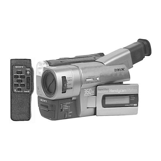
Photo: CCD-TRV66
For MECHANISM ADJUSTMENT, refer to
the "8mm Video MECHANICAL
ADJUSTMENT MANUAL
SPECIFICATIONS
VIDEO CAMERA RECORDER
RMT-708
US Model
Hong Kong Model
Brazilian Model
CCD-TRV66
Canadian Model
CCD-TRV63/TRV66
E Model
CCD-TRV66/TRV66PK
B MECHANISM
" (9-973-801-11).
Advertisement
Table of Contents

Related Manuals for Sony CCD-TRV63


Summary of Contents for Sony CCD-TRV63
- Page 1 CCD-TRV63/TRV66/TRV66PK RMT-708 SERVICE MANUAL US Model Hong Kong Model Brazilian Model CCD-TRV66 Ver 1.0 1998.12 Canadian Model CCD-TRV63/TRV66 E Model CCD-TRV66/TRV66PK Photo: CCD-TRV66 B MECHANISM • The CCD-TRV66PK is made by combining the CCD-TRV66 For MECHANISM ADJUSTMENT, refer to (E model), carrying bag.
- Page 2 MARK ! ON THE SCHEMATIC DIAGRAMS AND IN THE PARTS CRITIQUES POUR LA SÉCURITÉ DE FONCTIONNEMENT. NE LIST ARE CRITICAL TO SAFE OPERATION. REPLACE THESE REMPLACER CES COMPOSANTS QUE PAR DES PIÈSES SONY COMPONENTS WITH SONY PARTS WHOSE PART NUMBERS DONT LES NUMÉROS SONT DONNÉS DANS CE MANUEL OU APPEAR AS SHOWN IN THIS MANUAL OR IN SUPPLEMENTS DANS LES SUPPÉMENTS PUBLIÉS PAR SONY.
-
Page 3: Table Of Contents
TABLE OF CONTENTS SERVICE NOTE 2-6. Video Light ······································································ 2-8 2-7. CF-56 Board ···································································· 2-8 POWER SUPPLY DURING REPAIRS ····························· 6 2-8. How to Identify Drum and Note ······································ 2-8 TO TAKE OUT A CASSETTE WHEN NOT EJECT 2-9. Circuit Boards Location ·················································· 2-9 (FORCE EJECT) ································································... - Page 4 • PD-105 (RGB Decoder, LCD)(1/2) Contrast Adjustment (PD-105 board) ···························· 5-26 Schematic Diagram ······································· 4-63 V-COM Level Adjustment (PD-105 board) ·················· 5-27 • PD-105 (Timing Generator, Back Light Drive)(2/2) Color Adjustment (PD-105 board) ································ 5-27 Schematic Diagram ······································· 4-67 V-COM Adjustment (PD-105 board) ···························· 5-28 •...
- Page 5 6-1-2. Cabinet (R) Block Assembly ··········································· 6-2 6-1-3.LCD Block Assembly ······················································ 6-3 6-1-4.Cabinet (L) Block and Main Boards Assembly ··············· 6-4 6-1-5. EVF Block Assembly ······················································ 6-5 6-1-6. Cassette Compartment Assembly ···································· 6-6 6-1-7. LS Chassis Assembly ······················································ 6-7 6-1-8. Mechanism Chassis Assembly ········································ 6-8 6-2.
-
Page 6: Service Note
SERVICE NOTE POWER SUPPLY DURING REPAIRS In this unit, about 10 seconds after power is supplied (8.4V) to the Battery switch battery terminal using the service power cord (J-6082-223-A), the power is shut off so that the unit cannot operate. This following two methods are available to prevent this. -
Page 7: Self-Diagnosis Function
SELF-DIAGNOSIS FUNCTION Self-diagnosis Display Self-diagnosis Function When problems occur while the unit is operating, the counter of the When problems occur while the unit is operating, the self-diagnosis viewfinder or Display window shows a 4-digit display consisting function starts working, and displays on the viewfinder or Display window what to do. -
Page 8: Self-Dignosis Code Table
Self-diagnosis Code Table Self-diagnosis Code Block Detailed Symptom/State Correction Function Code Condensation. Remove the cassette, and insert it again after one hour. Video head is dirty. Clean with the optional cleaning cassette. Non-standard battery is used. Use the InfoLITHIUM battery. LOAD direction. - Page 9 Self-diagnosis Code Block Detailed Symptom/State Correction Function Code Inspect the lens block focus reset sensor (Pin !™ of CN551 of VC- 214 board) when focusing is performed when the control dial is Difficult to adjust focus rotated in the focus manual mode and the focus motor drive circuit (Cannot initialize focus.) (IC552 of VC-214 board) when the focusing is not performed.
-
Page 10: General
CCD-TRV63/TRV66/TRV66PK SECTION 1 This section is extracted from instruction GENERAL manual. (CCD-TRV63/TRV66 model) - Page 19 1-10...
- Page 20 1-11...
- Page 21 1-12...
- Page 22 1-13...
- Page 23 1-14...
- Page 24 1-15...
- Page 25 1-16...
- Page 26 1-17...
- Page 27 1-18...
- Page 28 1-19...
- Page 29 1-20E...
-
Page 30: Disassembly
CCD-TRV63/TRV66/TRV66PK SECTION 2 DISASSEMBLY The following flow chart shows the disassembly procedure. MECHANISM DECK check 2-1. MECHANISM DECK (Note) service position Note : Use the parts only which can be removed easily from outside of the MECHANISM DECK. LCD check 2-2. -
Page 31: Mechanism Deck
NOTE: Follow the disassembly procedure in the numerical order given. 2-1. MECHANISM DECK Remove it in the direction 1 Two screws of the arrow b . (M2 × 4), lock ace, p2 !• Screw (M2 × 4), lock ace, p2 2 Cassette lid assembly @¢... -
Page 32: Lcd Unit, Pd-105 Board
2-2. LCD UNIT, PD-105 BOARD 7 P cabinet (C)(93) 8 Two tapping screws (B2 × 8) 6 Claws 4 Two screws (M2 × 4) 3 Rotate it by 90 ° in the direction of the arrow. Indication LCD block assembly !¡... -
Page 33: Lens Block
2-3. LENS BLOCK @™ Flexible board (from LENS block) (24P) @º Screw (M2 × 3), @¡ Screw (M2 × 3), lock ace, p2 lock ace, p2 !• FP-54 flexible board @£ LENS block !¶ VL-23 board !™ Screw !§ Screw (M2 ×... -
Page 34: Evf Block, Vf-129 Board
2-4. EVF BLOCK, VF-129 BOARD 5 EVF block assembly 9 Finder (S) assembly 8 Rotate it in the direction of 3 FFC-256 the arrow b and remove it flexible flat cable (4P) in the direction of the arrow c . 6 Screw 7 Slide the button in the !∞... -
Page 35: Mechanism Deck, Vc-214, Dd-117 Boards
2-5. MECHANISM DECK, VC-214, DD-117 BOARDS 5 Screw (M2 × 4), Remove it in the direction of the arrow a . lock ace, p2 Remove it in the direction of the arrow b . Remove it gently as a thin flexible board is held by a claw. - Page 36 [MECHANISM DECK, VC-214, DD-117 BOARDS CHECK SERVICE POSITION] Battery panel (P) AC IN assembly Control switch block (SS-8500) AC POWER ADAPTOR Base 2 Adjustment remote DC IN commander (RM-95) DD-117 board Extension cable (J-6082-439-A) (70P) Control switch block (FK-8500) Mechanism deck Base 1 CPC-7 jig (J-6082-382-A)
-
Page 37: Video Light
2-6. VIDEO LIGHT 3 Halogen lamp 2 Remove the lamp holder in the direction of the arrow a . 1 Remove the claws 2-7. CF-56 BOARD Note : When attaching it. Align the switch position as shown. 5 FFC-256 flexible flat cable (4P) 6 Speaker harness (2P) 7 Six tapping !º... -
Page 38: Circuit Boards Location
2-9. CIRCUIT BOARDS LOCATION CD-209 (CCD IMAGER) VF-129 (B/W EVF) VL-23 (VIDEO LIGHT) MA-351 (STEREO MIC AMP, LASER LINK) DD-117 (DC/DC CONVERTER) PJ-92 (AV IN/OUT) SE-83 (STEADY SHOT) CF-56 (USER CONTROL) PD-105 RGB DECODER, LCD, TIMING GENERATOR, BACK LIGHT DRIVE VC-214 CAMERA PROCESSOR, Y/C PROCESSOR, FOCUS/ZOOM... -
Page 39: Flexible Boards Location
2-10.FLEXIBLE BOARDS LOCATION FP-49 CONTROL SWITCH BLOCK (FK-8500) FP-54 FP-46 (From S/T REEL SENSOR) (From CAPSTAN MOTOR) (From DRUM MOTOR) FP-43 (From LENS BLOCK) (From VIDEO HEAD) FP-44 From LOADING MOTOR, CONTROL SWITCH BLOCK MODE SWITCH (SS-8500) FFC-256 FP-62 FP-642 CONTROL SWITCH BLOCK (MR-8500) FFC-236... -
Page 40: Block Diagrams
CCD-TRV63/TRV66/TRV66PK SECTION 3 BLOCK DIAGRAMS 3-1. OVERALL BLOCK DIAGRAM... -
Page 41: Camera/Video Block Diagram
CCD-TRV63/TRV66/TRV66PK 3-2. CAMERA/VIDEO BLOCK DIAGRAM IC1401 7 IC1402 6 IC502 @§ IC001 $¶ IC001 1 CAMERA REC CAMERA REC CAMERA REC IC001 @¶,#¢ CAMERA REC 1.1Vp-p 1.2Vp-p IC202 !§ IC202 !£ CAMERA REC CAMERA REC 1 µsec/div, 0.1 V/div 0.1 µsec/div 0.3Vp-p... -
Page 42: Vtr/Camera Control Block Diagram
CCD-TRV63/TRV66/TRV66PK 3-3. VTR/CAMERA CONTROL BLOCK DIAGRAM IC402 1 20.0 MHz 1.7Vp-p IC402 $¶ 2.8Vp-p 30 Hz 3-10 3-11... -
Page 43: Servo Block Diagram
CCD-TRV63/TRV66/TRV66PK 3-4. SERVO BLOCK DIAGRAM IC801 !• IC802 9 IC801 ^¢ IC801 1,2,@ª 0.05Vp-p 3.9 msec 0.75Vp-p 0.1Vp-p 2 µsec 1.5Vp-p 180 Hz 1.25 µsec IC802 7 IC801 !¡ 0.1Vp-p 1.25 µsec IC801 4 2.8Vp-p 30 Hz 0.75Vp-p 2 µsec IC402 1 20.0 MHz... -
Page 44: Mode Control Block Diagram
CCD-TRV63/TRV66/TRV66PK CCD-TRV63/TRV66/TRV66PK 3-5. MODE CONTROL BLOCK DIAGRAM IC604 $º 3.2Vp-p 20.0 MHz IC604 %£ 3.2Vp-p 32.768 KHz 3-15 3-16 3-17... -
Page 45: Audio Block Diagram
CCD-TRV63/TRV66/TRV66PK 3-6. AUDIO BLOCK DIAGRAM IC751 $¡ IC751 @™ CAMERA REC/PB CAMERA REC/PB IR ON IR ON 0.22Vp-p 0.22Vp-p 0.5 µsec/div IC751 7 CAMERA REC/PB 0.18Vp-p 3.5795 MHz 3-19 3-20 3-21 3-22... -
Page 46: Lcd Block Diagram
CCD-TRV63/TRV66/TRV66PK 3-7. LCD BLOCK DIAGRAM IC5502 @¢ IC5502 @™ 2.0Vp-p 2.0Vp-p IC5502 @º 2.0Vp-p IC5502 8 IC5502 9 IC5502 !º IC5602 7 0.4Vp-p 0.3Vp-p 0.1Vp-p 5.0Vp-p 7.852 KHz IC5601 @§ 3.0Vp-p 5.79 MHz IC5601 #¶ 2.8Vp-p 3-23 3-24 3-25... -
Page 47: Evf Block Diagram
CCD-TRV63/TRV66/TRV66PK CCD-TRV63/TRV66/TRV66PK 3-8. EVF BLOCK DIAGRAM IC901 !¡ IC901 !§ 0.9Vp-p 2.4Vp-p IC901 !£ 1.1Vp-p IC901 3 2.0Vp-p 16.7 msec IC901 1,5 2.0Vp-p 16.7 msec IC901 7 1.1Vp-p 16.7 msec 3-27 3-28... -
Page 48: Power Block Diagram
CCD-TRV63/TRV66/TRV66PK 3-9. POWER BLOCK DIAGRAM 3-29 3-30 3-31 3-32E... -
Page 49: Frame Schematic Diagram-1
CCD-TRV63/TRV66/TRV66PK SECTION 4 PRINTED WIRING BOARDS AND SCHEMATIC DIAGRAMS 4-1. FRAME SCHEMATIC DIAGRAM-1 FRAME SCHEMATIC DIAGRAM (1/2) - Page 50 CCD-TRV63/TRV66/TRV66PK FRAME SCHEMATIC DIAGRAM-2 FRAME SCHEMATIC DIAGRAM (2/2)
-
Page 51: Ccd Imager
CCD-TRV63/TRV66/TRV66PK 4-2. PRINTED WIRING BOARDS AND SCHEMATIC DIAGRAMS CD-209 (CCD IMAGER) PRINTED WIRING BOARD — Ref. No. CD-209 Board; 10,000 Series — CD-209 BOARD THIS NOTE IS COMMON FOR WIRING BOARDS AND SCHEMATIC DIAGRAMS C1401 (In addition to this, the necessary note is printed in each block) - Page 52 CCD-TRV63/TRV66/TRV66PK VC-214 (CAMERA PROCESSOR, Y/C PROCESSOR, FOCUS/ZOOM MOTOR DRIVE, REC/PB HEAD AMP, VIDEO/INTERFACE, IR TRANSMITTER, MODE CONTROL, SERVO, HI CONTROL, SYSTEM CONTROL, AUDIO PROCESSOR) PRINTED WIRING BOARD — Ref. No. VC-214 Board; 1,000 Series — VC-214 BOARD (SIDE A) C006...
- Page 53 CCD-TRV63/TRV66/TRV66PK CCD-TRV63/TRV66/TRV66PK VC-214 BOARD (SIDE B) C001 A-15 C384 C-14 C827 A-11 Q016 B-15 R084 B-15 R521 D-14 R756 B-17 C004 A-14 C385 C-15 C828 A-11 Q017 A-15 R087 C-15 R526 D-14 R757 B-17 C005 B-14 C386 C-15 C829 A-11...
-
Page 54: Camera Processor
CCD-TRV63/TRV66/TRV66PK CCD-TRV63/TRV66/TRV66PK For schematic diagram • Refer to page 4-11 for printed wiring board. VC-214 BOARD (1/10) IC501 5 IC502 !º CAMERA REC/PB CAMERA REC LINE REC 3.0Vp-p 28.63562 MHz 2.9Vp-p 72 nsec IC501 !¡ IC502 !º PB CAMERA REC/PB 3.0Vp-p... - Page 55 CCD-TRV63/TRV66/TRV66PK For schematic diagram • Refer to page 4-11 for printed wiring board. • Refer to page 4-23 for waveforms. Y/C PROCESSOR 4-19 4-20 4-21 4-22 VC-214 (2/10)
- Page 56 CCD-TRV63/TRV66/TRV66PK CCD-TRV63/TRV66/TRV66PK For schematic diagram • Refer to page 4-11 for printed wiring board. VC-214 BOARD (2/10) !™ !§ !ª IC202 3 IC202 @£ IC202 #¶ CAMERA REC/PB CAMERA REC/PB LINE REC 0.3Vp-p 0.3Vp-p 0.45Vp-p !™ !§ @º IC202 3 IC202 @£...
-
Page 57: Rec/Pb Head Amp
CCD-TRV63/TRV66/TRV66PK For schematic diagram • Refer to page 4-11 for printed wiring board. • Refer to page 4-30 for waveforms. REC/PB HEAD AMP 4-27 4-28 4-29 VC-214 (4/10) -
Page 58: Video/Interface
CCD-TRV63/TRV66/TRV66PK For schematic diagram • Refer to page 4-11 for printed wiring board. VC-214 VC-214 BOARD (4/10) BOARD (5/10) @∞ #º #∞ CN001 !§, Q001 C IC151 3 IC151 @ª CAMERA REC CAMERA REC/PB CAMERA REC/PB 0.48Vp-p 2Vp-p 4.1 MHz 7.0Vp-p... -
Page 59: Ir Transmitter
CCD-TRV63/TRV66/TRV66PK CCD-TRV63/TRV66/TRV66PK For schematic diagram • Refer to page 4-11 for printed wiring board. VC-214 BOARD (6/10) $™ IC751 7 CAMERA REC/PB 0.18Vp-p 3.5795 MHz $£ IC751 @™ CAMERA REC/PB IR ON 0.22Vp-p 0.5 µsec/div $¢ IC751 $¡ CAMERA REC/PB IR ON 0.22Vp-p... -
Page 60: Mode Control
CCD-TRV63/TRV66/TRV66PK For schematic diagram • Refer to page 4-11 for printed wiring board. VC-214 BOARD (7/10) CAMERA REC/PB $∞ IC402 1 1.7Vp-p 20.0 MHz $§ IC402 $¶ 2.8Vp-p 30 Hz MODE CONTROL 4-36 4-37 4-38 VC-214 (7/10) - Page 61 CCD-TRV63/TRV66/TRV66PK For schematic diagram FP-249 (S/T REEL SENSOR), FP-356 (TOP SENSOR), FP-355 (TAPE LED) FLEXIBLE BOARD • Refer to page 4-11 for printed wiring board. PRINTED WIRING BOARD — Ref. No. FP-249, 356, 355 FLEXIBLE board; 5,000 series — VC-214...
- Page 62 CCD-TRV63/TRV66/TRV66PK VL-23 (VIDEO LIGHT) PRINTED WIRING BOARD For schematic diagram — Ref. No. VL-23 Board; 2,000 Series — • Refer to page 4-11 for printed wiring board. VC-214 BOARD (9/10) CAMERA REC/PB %™ IC604 $º 3.2Vp-p 20.0 MHz %£ IC604 %£...
-
Page 63: Audio
CCD-TRV63/TRV66/TRV66PK For schematic diagram • Refer to page 4-11 for printed wiring board. AUDIO 4-47 4-48 4-49 VC-214 (10/10) -
Page 64: Steady Shot), Pj-92 (Av In/Out)
CCD-TRV63/TRV66/TRV66PK SE-83 (STEADY SHOT), PJ-92 (AV IN/OUT) PRINTED WIRING BOARDS — Ref. No. SE-83, PJ-92 Board; 2,000 Series — SE-83 BOARD PJ-92 BOARD C451 C101 C452 C102 C453 C103 C454 C104 C457 C105 C458 C106 C459 C107 C460 C108 C461... -
Page 65: Steady Shot), Pj-92 (Av In/Out)
CCD-TRV63/TRV66/TRV66PK STEADY SHOT AV IN/OUT 4-53 4-54 SE-83 PJ-92... -
Page 66: Stereo Mic Amp, Laser Link
CCD-TRV63/TRV66/TRV66PK MA-351 (STEREO MIC AMP, LASER LINK) PRINTED WIRING BOARD — Ref. No. MA-351 Board; 2,000 Series — MA-351 BOARD C301 IC301 C302 IC322 C303 C304 J301 C305 C306 L301 C333 C334 Q301 C335 Q302 C336 Q303 C337 Q304 C338... - Page 67 CCD-TRV63/TRV66/TRV66PK STEREO MIC AMP, LASER LINK 4-57 4-58 4-59 MA-351...
-
Page 68: Rgb Decoder, Lcd, Timing Generator, Back Light Drive
CCD-TRV63/TRV66/TRV66PK PD-105 (RGB DECODER, LCD, TIMING GENERATOR, BACK LIGHT DRIVE) PRINTED WIRING BOARD — Ref. No. PD-105 Board; 10,000 Series — PD-105 BOARD C5501 L5504 R5647 D-8 C5502 L5601 R5648 D-5 C5503 L5603 R5651 D-8 C5504 L5604 R5652 D-8 C5505... -
Page 69: Rgb Decoder, Lcd)(1/2)
CCD-TRV63/TRV66/TRV66PK CCD-TRV63/TRV66/TRV66PK PD-105 BOARD (1/2) CAMERA REC/PB IC5801 2 3.0Vp-p 24.152 KHz IC5502 8 0.4Vp-p IC5502 9 0.3Vp-p IC5502 !º 0.1Vp-p IC5502 @º 2.0Vp-p IC5502 @™ 2.0Vp-p IC5502 @¢ 2.0Vp-p RGB DECODER, LCD 4-63 4-64 4-65 PD-105 (1/2) -
Page 70: Timing Generator, Back Light Drive)(2/2)
CCD-TRV63/TRV66/TRV66PK CCD-TRV63/TRV66/TRV66PK For schematic diagram • Refer to page 4-60 for printed wiring board. PD-105 BOARD (2/2) CAMERA REC/PB IC5601 @§ 3.0Vp-p 5.79 MHz IC5601 #¶ 2.8Vp-p !º IC5602 7 5.0Vp-p 7.852 KHz TIMING GENERATOR, BACK LIGHT DRIVE 4-67 4-68... -
Page 71: B/W Evf
CCD-TRV63/TRV66/TRV66PK VF-129 (B/W EVF) PRINTED WIRING BOARD — Ref. No. VF-129 Board; 3,000 Series — VF-129 BOARD VF-129 BOARD C901 R905 CAMERA REC/PB C902 R906 C903 R907 IC901 1,5 C904 R908 C905 R909 C906 R910 C907 R911 C908 R912 C909 R913 2.0Vp-p... -
Page 72: User Control
CCD-TRV63/TRV66/TRV66PK CF-56 (USER CONTROL) PRINTED WIRING BOARD — Ref. No. CF-56 Board; 2,000 Series — CF-56 BOARD BH001 D-5 R016 R020 C001 D-10 R022 C002 D-10 R023 C003 D-12 R025 R026 CN001 B-11 R029 B-12 CN002 A-14 R031 CN003 E-11... -
Page 73: User Control
CCD-TRV63/TRV66/TRV66PK USER CONTROL 4-75 4-76 4-77 CF-56/MR-8500... -
Page 74: Dc/Dc Converter
CCD-TRV63/TRV66/TRV66PK DD-117 (DC/DC CONVERTER) PRINTED WIRING BOARD — Ref. No. DD-117 Board; 2,000 Series — DD-117 BOARD C801 D806 Q828 R852 C802 D809 Q829 R853 C803 D810 Q830 R854 C804 D812 Q831 R859 C805 D813 Q832 R864 C806 D814 Q833... - Page 75 CCD-TRV63/TRV66/TRV66PK DD-117 BOARD CAMERA REC/PB IC801 4 0.75Vp-p 2 µsec IC801 ^¢ 0.75Vp-p 2 µsec DC/DC CONVERTER 4-81 4-82 4-83 4-84 DD-117...
- Page 76 CCD-TRV63/TRV66/TRV66PK CCD-TRV63/TRV66/TRV66PK CONTROL SWITCH BLOCK 4-88E FK-8500/SS-8500...
-
Page 77: Adjustments
CCD-TRV63/TRV66/TRV66PK SECTION 5 ADJUSTMENTS 5-1. CAMERA SECTION ADJUSTMENT 1-1. PREPARATIONS BEFORE ADJUSTMENT (CAMERA SECTION) 1-1-1. List of Service Tools • Oscilloscope • Color monitor • Vectorscope • Regulated power supply • Digital voltmeter Ref. No. Name Parts Code Usage Auto white balance adjustment/check... -
Page 78: Adjusting Items When Replacing Main Parts
1-1-2. Adjusting items when replacing main parts When replacing main parts, adjust the items indicated by r in the following table. Replacing parts Adjustment Adjusting item Section Initialization of D, E, F page data Camera HALL adj. Camera Flange back adj. Camera AGC gain calibration adj. -
Page 79: Preparations
1-1-3. Preparations Note 1: For details of how remove the cabinet and boards, refer to “2. DISASSEMBLY”. Note 2: When performing only the adjustments, the lens block and boards Pattern box need not be disassembled. Connect the equipment for adjustments according to Fig. 5-1-3. By setting the “Forced Camera Power ON mode”, the camera power can be turned ON even if the front panel block (MA- 351 board, power switch, microphone unit) has been removed. - Page 80 Note: Press the battery switch of the battery terminal using adhesive tape, etc. Color monitor Vector scope Regulated power supply (Note) Terminated at 75 Ω (8.4 ± 0.1Vdc) Need not connected CD-209 board CN1401 Lens block Battery terminal Adjustment remote commander Extension cable (16P, 0.5mm)
-
Page 81: Precaution
1-1-4. Precaution 1. Setting the Switch Unless otherwise specified, set the switches as follows and perform adjustments without loading cassette. POWER switch (MA-351 board) ......CAMERA DISPLAY (CF-56 board) ..........ON NIGHT SHOT switch (Lens block) ......... OFF FOCUS switch (MR-8500 block) ......MANUAL VIDEO LIGHT switch (MA-351 board) ...... -
Page 82: Initialization Of D, E, F Page Data
1-2. INITIALIZATION OF D, E, F PAGE DATA 3. D Page Table Note : Fixed data-1 : Initialized data. (Refer to “1. Initializing the D,E,F Page Data”.) 1. Initializing the D,E,F Page Data Fixed data-2 : Modified data. (Refer to “2. Modification of D, E, F Note: If the D,E,F page data has been initialized, “Modification of D, E, F Page Data”.) Page Data”... - Page 83 4. F Page table Address Remark Note : Fixed data-1 : Initialized data. (Refer to “1. Initializing the D,E,F Initial value Page Data”.) Fixed data-2 Fixed data-2 : Modified data. (Refer to “2. Modification of D, E, F Page Data”.) Fixed data-1 Address Remark...
- Page 84 Address Remark Address Remark Initial value Initial value Fixed data-1 REC L level adj. (Initialized data) HALL adj. Max gain adj. Fixed data-1 (Initialized data) REC C current adj. Color reproduction adj. Fixed data-1 Fixed data-1 (Initialized data) Color reproduction adj. Fixed data-1 (Initialized data) Auto white balance adj.
- Page 85 Address Remark Address Remark Initial value Initial value Fixed data-1 Fixed data-1 (Initialized data) (Initialized data) Fixed data-2 Fixed data-1 Flange back adj. Color reproduction adj. Fixed data-1 (Initialized data) Table. 5-1-3. Fixed data-2 Fixed data-1 (Initialized data)
- Page 86 5. E Page Table Address Remark Note : Fixed data-1 : Initialized data. (Refer to “1. Initializing the D,E,F Initial value Page Data”.) Fixed data-1 Fixed data-2 : Modified data. (Refer to “2. Modification of D, E, F Page Data”.) (Initialized data) Address Remark...
- Page 87 Address Remark Address Remark Initial value Initial value Fixed data-1 Fixed data-1 (Initialized data) (Initialized data) Fixed data-2 (Modified data, copy the data built in the same model.) Fixed data-1 (Initialized data) Fixed data-2 (Modified data, copy the data built in the same model.) Fixed data-1 (Initialized data)
- Page 88 Address Remark Initial value Fixed data-1 (Initialized data) Fixed data-2 (Modified data, copy the data built in the same model.) Fixed data-1 Table. 5-1-4. 5-12...
-
Page 89: Camera System Adjustments
1-3. CAMERA SYSTEM ADJUSTMENTS Before perform the camera system adjustments, Check that the specified value of “28MHz Origin Oscillation Adjustment”, “Y OUT level Adjustment” and “C OUT level Adjustment” of “VIDEO SYSTEM ADJUSTMENT” are satisfied. 1. HALL Adjustment 2. Flange Back Adjustment For detecting the position of the lens iris, adjust the hall AMP gain The inner focus lens flange back adjustment is carried out and offset. -
Page 90: Flange Back Adjustment (2)
2-2. Flange Back Adjustment (2) 3. Flange Back Check Perform this adjustment after performing “Flange Back Adjustment Subject Siemens star (1)”. (2.0 m from the front of the lens) Subject Subject more than 500m away (Luminance : approx. 200 lux) (Subjects with clear contrast such as Measurement Point Check operation on TV monitor... -
Page 91: Picture Frame Setting
4. Picture Frame Setting 5. AGC Gain Calibration Adjustment Subject Color bar chart Subject Clear chart (Color reproduction adjustment frame) (Color reproduction adjustment frame) (1.5m from the front of the lens) Adjustment Page Measurement Point Video output terminal Adjustment Address 2E, 2F, 30, 31 Measuring Instrument Oscilloscope and TV monitor... -
Page 92: Color Reproduction Adjustment
6. Color Reproduction Adjustment 7. IRIS IN/OUT Adjustment Adjust the color Separation matrix coefficient so that proper color For the unit to judge if the white balance is indoors or outdoors in reproduction is produced. auto white balance operations, measure the light level and write it in the EEPROM. -
Page 93: Max Gain Adjustment
8. MAX GAIN Adjustment 9. Auto White Balance Standard Data Input Setting the minimum illumination. Subject Clear chart If it is not consistent, the image level required for taking subjects in (Color reproduction adjustment frame) low illuminance will not be produced (dark). Adjustment Page Subject Clear chart... -
Page 94: Auto White Balance Adjustment
10. Auto White Balance Adjustment Adjust to the proper auto white balance output data. If it is not correct, auto white balance and color reproducibility will be poor. Subject Clear chart (Color reproduction adjustment frame) Filter Filter C14 for color temperature correction Measurement Point DDS display of LCD or TV monitor... -
Page 95: White Balance Check
11. White Balance Check Subject Clear chart (Color reproduction adjustment frame) Filter Filter C14 for color temperature correction ND filter 1.0 and 0.3 Measurement Point Video output terminal Measuring Instrument Vectorscope Specified Value Fig. 5-1-10. A to C Fig. 5-1-10. (A) Switch setting: NIGHT SHOT .............. -
Page 96: Angular Velocity Sensor Sensitivity Preset And Steady Shot Check
12. Angular Velocity Sensor Sensitivity Preset and Steady shot check Check the output of the angular velocity sensor. Precautions on the Parts Replacement There are two types of repair parts. Type A ENC03JA Type B ENC03JB Replace the broken sensor with a same type sensor. If replace with other type parts, the image will vibrate up and down or left and right during hand-shake correction operations. -
Page 97: Horizontal Slant Check
1-4. MONOCHROME ELECTRONIC VIEWFINEDER 1-4-2. Centering Adjustment SYSTEM ADJUSTMENT Mode Playback Signal Alignment tape : 1-4-1. Horizontal Slant Check For checking operation Mode Playback (WR5-5NSP) Monoscope section Signal Alignment tape : For checking operation Specified Value ± 4% (WR5-5NSP) Monoscope section Adjusting method: Use the centering adjustment ring and adjust so that the left, Specified Value... -
Page 98: Aberration Adjustment
1-4-4. Aberration Adjustment 1-4-5. Horizontal Amplitude Adjustment (VF-129 board) Mode VTR stop Mode Playback Signal Dot pattern Signal Alignment tape : 2 × a1 For checking operation Specified Value 0.8 × a2 (WR5-5NSP) Monoscope section Adjusting method: Adjusting Element C909 (SOL901) 1) Adjust the aberration adjustment ring so that the tracing of the Specified Value 10 ±... -
Page 99: Vertical Amplitude Adjustment (Vf-129 Board)
1-4-6. Vertical Amplitude Adjustment (VF-129 board) 1-4-7. Brightness Adjustment (VF-129 board) Mode Playback Mode Playback Signal Alignment tape : Signal Alignment tape : For checking operation For checking operation (WR5-5NSP) (WR5-5NSP) Monoscope section Monoscope section Adjusting Element RV903 Adjusting Element RV904 Specified Value 10 ±... -
Page 100: Lcd System Adjustment
1-5. LCD SYSTEM ADJUSTMENT 1. LCD Initial Data Input Note 1: The back light (fluorescent tube) is driven by a high voltage AC Mode VTR stop power supply. Therefore, do not touch the back light holder to Signal Arbitrary avoid electrical shock. Note 2: When replacing the LCD unit, be careful to prevent damages Adjustment Page caused by static electricity. -
Page 101: Vco Adjustment (Pd-105 Board)
2. VCO Adjustment (PD-105 board) 3. D range Adjustment (PD-105 board) Set the VCO free-run frequency. If deviated, the LCD screen will Set the D range of the RGB decoder used to drive the LCD to the be blurred. specified value. If deviated, the LCD screen will become blackish or saturated (whitish). -
Page 102: Bright Adjustment (Pd-105 Board)
4. Bright Adjustment (PD-105 board) 5. Contrast Adjustment (PD-105 board) Set the level of the VIDEO signal for driving the LCD to the specified Set the level of the VIDEO signal for driving the LCD to the specified value. If deviated, the screen image will be blackish or saturated value. -
Page 103: V-Com Level Adjustment (Pd-105 Board)
6. V-COM Level Adjustment (PD-105 board) 7. Color Adjustment (PD-105 board) Set the common electrode drive signal level of LCD to the specified Set the color saturation to the standard value. If deviated, the color value. will be to dark or light. Mode VTR stop Mode... -
Page 104: V-Com Adjustment (Pd-105 Board)
8. V-COM Adjustment (PD-105 board) 9. White Balance Adjustment (PD-105 board) Set the DC bias of the common electrode drive signal of LCD to the Correct the white balance. specified value. If deviated, the LCD screen color cannot be reproduced. If deviated, the LCD display will move, producing flicker and Mode VTR stop... -
Page 105: Mechanism Section Adjustment
5-2. MECHANISM SECTION ADJUSTMENT Mechanism Section adjustments, checks, and replacement of mechanism parts, refer to the separate volume “8mm Video Mechanism Adjustment Manual B Mechanism ”. 2-1. OPERATING WITHOUT CASSETTE 2-2. TAPE PATH ADJUSTMENT Refer to “Section 2. DISASSEMBLY” and supply the power 1. -
Page 106: Video Section Adjustment
5-3. VIDEO SECTION ADJUSTMENTS 3-1. PREPARATIONS BEFORE ADJUSTMENTS Use the following measuring instruments for video section adjustments. 3-1-1. Equipment to Required 1) TV monitor 2) Oscilloscope (dual-phenomenon, band width above 30 MHz with delay mode) (Unless specified otherwise, use a 10 : 1 probe.) 3) Frequency counter 4) Pattern generator with video output terminal... -
Page 107: Precautions On Adjusting
3-1-2. Precautions on Adjusting 3-1-3. Adjusting Connectors The adjustments of this unit are performed in the VTR mode Some of the adjusting points of the video section are concentrated or camera mode. at VC-214 board CN910. Connect the measuring instruments via To set to the VTR mode, set the power switch to “VTR”... -
Page 108: Connecting The Equipments
3-1-4. Connecting the Equipments Connecting the measuring instruments as shown in Fig. 5-3-2 and perform the adjustments. Connecting the TV Monitor and Regulated Power Supply Battery terminal Main Unit TV monitor Regulated power supply 8.4 0.1Vdc VIDEO Connect when using the camera mode or playing back. -
Page 109: Alignment Tape
3-1-5. Alignment Tape 3-1-6. Input/Output Level and Impedance The following table lists alignment tapes which are available. Video input/output Use the tape specified in the signal column for each adjustment. Phono jack, 1 Vp-p, 75Ω, If the type of tape to be used for checking operations is not specified, unbalanced, sync negative use whichever type. -
Page 110: System Control System Adjustment
3-2. SYSTEM CONTROL SYSTEM ADJUSTMENT 1. Initialization of D, E, F Page Data If the D, E, F page data is erased due to some reason, perform “1-2. INITIALIZATION OF D, E, F PAGE DATA”, of “5-1. CAMERA SECTION ADJUSTMENT” 2. -
Page 111: Servo System Adjustments
3-3. SERVO SYSTEM ADJUSTMENTS 2. Switching Position Adjustment (VC-214 board) 1. CAP FG Offset Adjustment (VC-214 board) If deviated in this case causes switching noise or jitter on the played Improve the capstan servo characteristic. If it is not correct. jitters back screen. -
Page 112: Video System Adjustments
3-4. VIDEO SYSTEM ADJUSTMENTS 2. AFC f Adjustment (VC-214 board) Adjust the pull-in range of the A/D converted clock generator during Video system adjustments must be performed in the following order. playback. Mode VTR stop [Adjusting Order] Signal No signal 28MHz origin oscillation adjustment Pin 4 of CN910 (AFC f0) Measurement Point... -
Page 113: Filter F Adjustment (Vc-214 Board)
3. Filter f Adjustment (VC-214 board) 4. Y OUT Level Adjustment (VC-214 board) Adjust the f frequency of the IC151 built-in filter. Set the Y signal output level. (Adjust the D/A converter out put level of IC151.) Mode VTR stop Mode VTR stop Signal... -
Page 114: C Out Level Adjustment (Vc-214 Board)
5. C OUT Level Adjustment (VC-214 board) 6. RP Filter f Adjustment (VC-214 board) Set the chroma signal output level. (Adjust the D/A converter out Adjust the LPF of the playback RF amplifier (IC001). put level of IC151.) Mode VTR stop Mode VTR stop Signal... -
Page 115: Rec Y Current Adjustment (Vc-214 Board)
7. REC Y Current Adjustment (VC-214 board) Adjust the Y FM signal recording current. Mode VTR recording (SP mode) Signal No signal Pin !º of CN910 (REC RF) Measurement Point Measuring Instrument Oscilloscope (20 MHz BW LIMIT: OFF) Adjustment Page Adjustment Address 73 to 7A Specified Value... -
Page 116: Rec L Level Adjustment (Vc-214 Board)
8. REC L Level Adjustment (VC-214 board) Set the recording levels of the REC AFM signal and REC ATF signal. VC-214 BOARD If the level is too low, the audio S/N will deteriorated, tracking will not be stable, or SP/LP will not be discriminated properly. If too high, color beets will be produced on the self-recording / playback image. -
Page 117: Rec C Current Adjustment (Vc-214 Board)
9. REC C Current Adjustment (VC-214 board) Set the recording current levels of the REC Chroma signal. If it is too low, chroma signal noise in played back picture will increased. If too high, Y signal noises will increase and white modulation noises will be produced. -
Page 118: Ir Transmitter Adjustments
3-5. IR TRANSMITTER ADJUSTMENTS 2. IR Video Deviation Adjustment (VC-214 board) Mode Camera standby Adjust using a IR receiver jig (J-6082-383-A). Subject Arbitrary Note : If the distance between the IR receiver jig and the camcorder is Measurement Point VIDEO OUT terminal of IR receiver jig below 1m, cover the LASER LINK emitter with a ND filter. -
Page 119: Ir Audio Deviation Adjustment (Vc-214 Board)
3. IR Audio Deviation Adjustment (VC-214 board) Mode VTR recording Signal Audio signal : 400Hz, –7.5dBs : L or R of AUDIO terminal Video signal : Color bar signal : VIDEO terminal Measurement Point AUDIO L terminal and AUDIO R terminal of IR receiver jig (Terminated at 47kΩ) Measuring Instrument... -
Page 120: Audio System Adjustment
3-6. AUDIO SYSTEM ADJUSTMENT [Connecting the measuring instruments for the audio] • Perform the adjustment using color bar signal as a video signal input for the VIDEO terminal. Connect the audio system measuring instruments in addition to the • The items to be adjusted for the R channel will be indicated within video system measuring instruments as shown in Fig. -
Page 121: Mhz Deviation Adjustment (Vc-214 Board)
1. 1.5 MHz Deviation Adjustment (VC-214 board) 2. 1.7 MHz Deviation Adjustment (VC-214 board) Sets the spectrum of the L-ch ((L+R)/2 signal) level modulated Sets the spectrum of the R-ch ((L-R)/2 signal) level modulated during during recording. If deviated, the crosstalk signal of the audio signal recording. -
Page 122: Bpf F0 Adjustment (Vc-214 Board)
3. BPF f0 Adjustment (VC-214 board) Sets the BPF passing frequency so that the AFM signal can separate from the playback RF signal properly. If deviated. the mono/stereo mode will be differentiated incorrectly, and noises and distortions will increase during high volume playback. Mode Playback Signal... -
Page 123: Service Mode
5-4. SERVICE MODE 4-1. ADJUSTMENT REMOTE COMMANDER 2. Precautions Upon Using the Adjustment Remote Commander The adjustment remote commander is used for changing the calculation coefficient in signal processing, EVR data, etc. The Mishandling of the adjustment remote commander may erase the correct adjustment data at times. -
Page 124: Data Process
4-2. DATA PROCESS The calculation of the DDS display and the adjustment remote commander display data (hexadecimal notation) are required for obtaining the adjustment data of some adjustment items. In this case, after converting the hexadecimal notation to decimal notation, calculate and convert the result to hexadecimal notation, and use it as the adjustment data. -
Page 125: Service Mode
4-3. SERVICE MODE Note: After the completion of the all adjustments, cancel the service mode by either of the following ways. Unplug the main power supply and remove the lithium battery. (In this case, date and time and menu setting have been set by users are canceled. -
Page 126: Emergency Memory Address
2. Emergency Memory Address 2-1. EMG code (Emergency code) The codes shown in the following table which correspond to errors that occur are recorded in addresses 10, 14, and 18. Page F Address 10 to 1B Code Type of Emergency Address Contents No error... -
Page 127: Msw Codes
2-2. MSW codes • The lower parts of the data of addresses 12, 16 and 1A represent the MSW codes (mode switch, mechanism position) when errors occurs. • The upper parts of the data of addresses 12, 16 and 1A represent, when the mechanism position is to be moved, the MSW codes at the start of movement (when moving the loading motor). -
Page 128: Bit Value Discrimination
3. Bit Value Discrimination Bit values must be discriminated using the display data of the Display on the Bit values adjustment remote commander for the following items. Us the table adjustment bit3 bit2 bit1 bit0 below to discriminate if the bit value is “1” or “0”. remote commander bit7... -
Page 129: Record Of Use Check
6. Record of Use check Page 2 Address A2 to AA Function Remarks Drum rotation Hour (H) 1000th place digit and 100th place digit of counted time (decimal digit) counted time Hour (L) 10th place digit and 1st place digit of counted time (decimal digit) (BCD code) Minute User initial power... -
Page 130: Switch Check (2)
8. Switch check (2) Page 2 Address 60 to 66 Using method: 1) Select page: 2, address: 60 to 66. 2) By discriminating the display data, the pressed key can be discriminated. Data Address 00 to 0B 0C to 23 24 to 3E 3F to 5C 5D to 80... -
Page 131: Repair Parts List
CCD-TRV63/TRV66/TRV66PK SECTION 6 REPAIR PARTS LIST 6-1. EXPLODED VIEWS NOTE: • -XX, -X mean standardized parts, so they may • The mechanical parts with no reference number The components identified by mark ! or have some differences from the original one. -
Page 132: Cabinet (R) Block Assembly
6-1-2. CABINET (R) BLOCK ASSEMBLY SP901 supplied supplied 57 58 Ref. No. Part No. Description Remarks Ref. No. Part No. Description Remarks 1-475-621-11 SWITCH BLOCK, CONTROL(MR-8500) 3-959-978-02 CUSHION, PANEL 3-948-339-61 TAPPING 3-053-706-01 COVER (R) (93), HINGE A-7073-841-A CF-56 BOARD, COMPLETE 3-053-684-01 GUIDE (B) (93), TILT 1-672-668-21 FP-62 FLEXIBLE BOARD 3-965-367-01 SPACER, SP... -
Page 133: 6-1-3.Lcd Block Assembly
6-1-3. LCD BLOCK ASSEMBLY supplied LED901 supplied ND901 LCD901 Ref. No. Part No. Description Remarks Ref. No. Part No. Description Remarks 4-981-286-01 SCREW (M1.7X2) (IB LOCK) 3-053-695-11 CABINET (C) (93), P (TRV63) 1-668-963-21 FP-642 FLEXIBLE BOARD 3-053-703-01 WINDOW (93), LCD (TRV66/TRV66PK) 3-987-625-11 COVER (M), HINGE 3-053-703-21 WINDOW (93), LCD (TRV63) X-3949-335-7 CABINET (M (93)) ASSY, P... -
Page 134: 6-1-4.Cabinet (L) Block And Main Boards Assembly
6-1-4. CABINET (L) BLOCK AND MAIN BOARDS ASSEMBLY supplied J001 supplied supplied supplied Ref. No. Part No. Description Remarks Ref. No. Part No. Description Remarks * 151 3-975-522-11 COVER, JACK A-7073-835-A DD-117 (VIB) BOARD, COMPLETE X-3948-315-1 CABINET (L) ASSY X-3947-199-1 LID ASSY, CASSETTE (TRV63/TRV66:US,CND) 3-052-815-01 BELT (ES), GRIP X-3948-331-1 LID ASSY, CASSETTE 3-679-362-11 SCREW... -
Page 135: Evf Block Assembly
6-1-5. EVF BLOCK ASSEMBLY V901 supplied supplied IC1401 224 225 M905 supplied M906 Be sure to read “Precautions upon replacing CCD imager” on page 4-9 when changing the CCD imager. Ref. No. Part No. Description Remarks Ref. No. Part No. Description Remarks 3-948-339-01 SCREW, TAPPING... -
Page 136: Cassette Compartment Assembly
6-1-6. CASSETTE COMPARTMENT ASSEMBLY LS CHASSIS ASSEMBLY (See page 6-7) MECHANISM CHASSIS ASSEMBLY (See page 6-8) Ref. No. Part No. Description Remarks Ref. No. Part No. Description Remarks A-7040-421-A DAMPER ASSY X-3949-383-1 GEAR ASSY (E), GOOSENECK 7-624-102-04 STOP RING 1.5, TYPE -E 3-947-503-01 SCREW (M1.4X2.5) X-3949-153-2 CASSETTE COMPARTMENT ASSY 3-727-176-01 WASHER, STOPPER... -
Page 137: Ls Chassis Assembly
6-1-7. LS CHASSIS ASSEMBLY S002 S001 D001 FP-249 (not supplied) Ref. No. Part No. Description Remarks Ref. No. Part No. Description Remarks A-7040-419-A BASE (S) BLOCK ASSY, GUIDE 3-965-579-01 ROLLER, PINCH PRESS A-7040-418-B BASE (T) BLOCK ASSY, GUIDE 3-965-563-01 GEAR, T SOFT 3-965-559-01 STOPPER (T) 3-965-565-01 CLAW, T SOFT 3-965-557-01 STOPPER (T), GB... -
Page 138: Mechanism Chassis Assembly
6-1-8. MECHANISM CHASSIS ASSEMBLY Note TYPE A TYPE B (Direct bearing type) (Shaft press fit type) M901 Circular rib Radial rib (When a drum is viewed from the top.) 81 1 M903 (Note) M902 S901 Note Ref.No. M901 TYPE supplied SCREW ASSY, DRUM ATTACHED ∫... -
Page 139: Electrical Parts List
CD-209 CF-56 6-2. ELECTRICAL PARTS LIST NOTE: • Due to standardization, replacements in the • RESISTORS When indicating parts by reference number, parts list may be different from the parts All resistors are in ohms. please include the board name. specified in the diagrams or the components METAL: metal-film resistor The components identified by mark ! or... - Page 140 CF-56 DD-117 Ref. No. Part No. Description Remarks Ref. No. Part No. Description Remarks S010 1-771-138-61 SWITCH, KEY BOARD (MENU) C848 1-164-506-11 CERAMIC CHIP 4.7uF S012 1-771-029-21 SWITCH, TACTILE (EXPOSURE) C849 1-135-149-21 TANTALUM CHIP 2.2uF S013 1-771-138-61 SWITCH, KEY BOARD (END SEARCH) C850 1-135-149-21 TANTALUM CHIP 2.2uF S015...
- Page 141 DD-117 Ref. No. Part No. Description Remarks Ref. No. Part No. Description Remarks < COIL > Q842 8-729-037-52 TRANSISTOR 2SC4738F-Y/GR(TPL3) Q843 8-729-037-53 TRANSISTOR 2SA1832F-Y/GR(TPL3) L804 1-412-056-11 INDUCTOR CHIP 4.7uH Q844 8-729-037-53 TRANSISTOR 2SA1832F-Y/GR(TPL3) L805 1-409-532-41 INDUCTOR 33uH Q845 8-729-037-52 TRANSISTOR 2SC4738F-Y/GR(TPL3) L806 1-409-532-41 INDUCTOR 33uH Q847...
- Page 142 DD-117 FP-249 FP-355 Ref. No. Part No. Description Remarks Ref. No. Part No. Description Remarks R837 1-216-826-11 METAL CHIP 2.7K 1/16W R913 1-216-857-11 METAL CHIP 1/16W R838 1-216-837-11 METAL CHIP 1/16W R914 1-216-811-11 METAL CHIP 1/16W R839 1-216-837-11 METAL CHIP 1/16W R915 1-218-911-11 RES,CHIP...
- Page 143 R352 1-216-839-11 METAL CHIP 1/16W < DIODE > D301 8-719-061-86 DIODE DCR2810 D302 8-749-060-65 DIODE DCC3810 D303 8-719-061-82 DIODE TLSU1002(TPX1,SONY) Note : Note : D305 8-719-073-01 DIODE MA111-(K8).S0 The components identified by Les composants identifiés par D321 8-719-073-03 DIODE MA8082-(K8).S0...
- Page 144 MA-351 PD-105 Ref. No. Part No. Description Remarks Ref. No. Part No. Description Remarks R353 1-216-839-11 METAL CHIP 1/16W C5622 1-107-682-11 CERAMIC CHIP R354 1-216-829-11 METAL CHIP 4.7K 1/16W C5623 1-107-826-91 CERAMIC CHIP 0.1uF R355 1-216-833-11 METAL CHIP 1/16W C5624 1-107-688-11 TANTAL.
- Page 145 PD-105 PJ-92 Ref. No. Part No. Description Remarks Ref. No. Part No. Description Remarks < RESISTOR > R5692 1-216-851-11 METAL CHIP 330K 1/16W R5694 1-216-839-11 METAL CHIP 1/16W R5501 1-216-840-11 METAL CHIP 1/16W R5695 1-216-833-11 METAL CHIP 1/16W R5505 1-216-841-11 METAL CHIP 1/16W R5697 1-216-864-11 METAL CHIP...
- Page 146 PJ-92 SE-83 VC-214 Ref. No. Part No. Description Remarks Ref. No. Part No. Description Remarks < COIL > < RESISTOR > L101 1-414-072-11 INDUCTOR 1uH R451 1-216-837-11 METAL CHIP 1/16W L102 1-216-295-91 SHORT 0 (Note) R452 1-216-837-11 METAL CHIP 1/16W L103 1-216-295-91 SHORT 0 (Note)
- Page 147 VC-214 Ref. No. Part No. Description Remarks Ref. No. Part No. Description Remarks C060 1-163-809-11 CERAMIC CHIP 0.047uF C191 1-162-970-11 CERAMIC CHIP 0.01uF C061 1-162-970-11 CERAMIC CHIP 0.01uF C192 1-119-750-11 TANTAL. CHIP 22uF 6.3V C062 1-162-926-11 CERAMIC CHIP 82PF C202 1-135-259-11 TANTAL.
- Page 148 VC-214 Ref. No. Part No. Description Remarks Ref. No. Part No. Description Remarks C331 1-107-826-91 CERAMIC CHIP 0.1uF C518 1-162-964-11 CERAMIC CHIP 0.001uF C332 1-109-982-11 CERAMIC CHIP C519 1-107-826-91 CERAMIC CHIP 0.1uF C334 1-115-467-11 CERAMIC CHIP 0.22uF C520 1-162-970-11 CERAMIC CHIP 0.01uF C336 1-109-982-11 CERAMIC CHIP...
- Page 149 VC-214 Ref. No. Part No. Description Remarks Ref. No. Part No. Description Remarks C627 1-164-227-11 CERAMIC CHIP 0.022uF C823 1-164-156-11 CERAMIC CHIP 0.1uF C628 1-162-919-11 CERAMIC CHIP 22PF C824 1-164-227-11 CERAMIC CHIP 0.022uF C629 1-162-917-11 CERAMIC CHIP 15PF C825 1-162-964-11 CERAMIC CHIP 0.001uF C630 1-164-156-11 CERAMIC CHIP...
- Page 150 VC-214 Ref. No. Part No. Description Remarks Ref. No. Part No. Description Remarks FB402 1-500-329-11 INDUCTOR CHIP 0UH L203 1-414-754-11 INDUCTOR 10uH FB501 1-500-329-11 INDUCTOR CHIP 0UH L204 1-410-658-31 INDUCTOR CHIP 220uH FB503 1-500-284-21 INDUCTOR CHIP 0UH L205 1-412-955-11 INDUCTOR 22uH FB504 1-500-284-21 INDUCTOR CHIP 0UH L206...
- Page 151 VC-214 Ref. No. Part No. Description Remarks Ref. No. Part No. Description Remarks Q215 8-729-037-52 TRANSISTOR 2SC4738F-Y/GR(TPL3) R045 1-216-845-11 METAL CHIP 100K 1/16W Q217 8-729-037-53 TRANSISTOR 2SA1832F-Y/GR(TPL3) R046 1-216-821-11 METAL CHIP 1/16W Q301 8-729-045-78 TRANSISTOR RN1110F(TPL3) R047 1-216-864-11 METAL CHIP 1/16W Q302 8-729-045-78 TRANSISTOR RN1110F(TPL3)
- Page 152 VC-214 Ref. No. Part No. Description Remarks Ref. No. Part No. Description Remarks R152 1-216-822-11 METAL CHIP 1.2K 1/16W R248 1-216-822-11 METAL CHIP 1.2K 1/16W R154 1-216-822-11 METAL CHIP 1.2K 1/16W R249 1-216-833-11 METAL CHIP 1/16W R157 1-216-822-11 METAL CHIP 1.2K 1/16W R250...
- Page 153 VC-214 Ref. No. Part No. Description Remarks Ref. No. Part No. Description Remarks R428 1-216-841-11 METAL CHIP 1/16W R605 1-216-841-11 METAL CHIP 1/16W R429 1-216-811-11 METAL CHIP 1/16W R606 1-216-829-11 METAL CHIP 4.7K 1/16W R430 1-216-813-11 METAL CHIP 1/16W R607 1-216-857-11 METAL CHIP 1/16W R431...
- Page 154 VC-214 VF-129 Ref. No. Part No. Description Remarks Ref. No. Part No. Description Remarks R673 1-216-821-11 METAL CHIP 1/16W R813 1-216-851-11 METAL CHIP 330K 1/16W R675 1-216-821-11 METAL CHIP 1/16W R814 1-216-845-11 METAL CHIP 100K 1/16W R676 1-216-821-11 METAL CHIP 1/16W R815 1-216-841-11 METAL CHIP...
- Page 155 VF-129 VL-23 Ref. No. Part No. Description Remarks Ref. No. Part No. Description Remarks C906 1-162-638-11 CERAMIC CHIP R924 1-216-862-11 RES,CHIP 2.7M 1/16W C907 1-104-563-11 FILM CHIP 0.1uF R925 1-216-862-11 RES,CHIP 2.7M 1/16W C908 1-162-920-11 CERAMIC CHIP 27PF R926 1-216-821-11 METAL CHIP 1/16W C909 1-163-009-11 CERAMIC CHIP...
- Page 156 Ref. No. Part No. Description Remarks Ref. No. Part No. Description Remarks MISCELLANEOUS ACCESSORIES ************* *********** 1-517-857-11 LIGHT, VIDEO 1-467-574-21 REMOTE COMMANDER (RMT-708) 1-694-384-11 TERMINAL BOARD, BATTERY 1-475-599-11 ADAPTOR, AC 1-672-663-21 FP-49 FLEXIBLE BOARD 1-569-008-21 ADAPTOR, CONVERSION 2P 1-783-240-11 CABLE, FLEXIBLE FLAT (FFC-236) (TRV66:E,HK,BR/TRV66PK) 1-672-670-11 FP-43 FLEXIBLE BOARD 1-575-334-11 AV CONNECTING CABLE (1.5M)
- Page 157 Take a copy of CAMERA COLOR REPRODUCTION FRAME and Parts referencesheets with a clear sheet for use. CCD-TRV63/TRV66/TRV66PK 〈PARTS REFERENCE SHEET〉 You can find the parts position of location of mount locations applying to VC-214 board of a set. VC-214...
- Page 158 CCD-TRV63/TRV66/TRV66PK Sony Corporation 98L1629-1 Printed in Japan ©1998.12 Personal A&V Products Company 9-974-126-11 Published by Quality Engineering Dept. — 246 — (Osaki East)
Need help?
Do you have a question about the CCD-TRV63 and is the answer not in the manual?
Questions and answers