Table of Contents
Advertisement
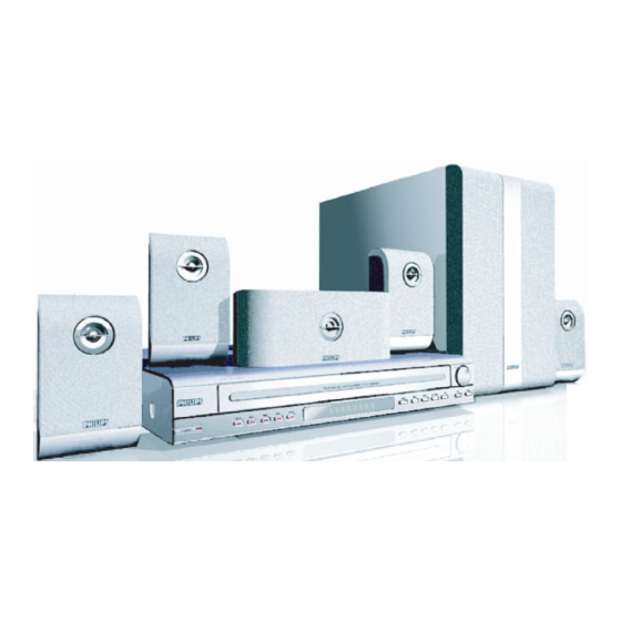
DVD Player
CLASS 1
LASER PRODUCT
Contents
1
2
3
4
5
6
7
© Copyright 2005 Philips Consumer Electronics B.V. Eindhoven, The Netherlands.
All rights reserved. No part of this publication may be reproduced, stored in
a retrieval system or transmitted, in any form or by any means, electronic,
mechanical, photocopying, or otherwise without the prior permission of Philips.
Published by KC-TE 0519 AV Systems
Version 1.0
Page
Contents
2
2
3
4
5
7
8
8
8
10
10
13
14
15
15
15
16
17
17
18
19
19
20
21
22
9
22
23
23
Printed in the Netherlands
HTS5500C/37/55
Subject to modifi cation
Page
24
25
26
27
28
29
30
31
31
32
33
34
35
36
37
38
39
40
41
42
43
44
45
46
47
47
48
49
50
51
53
EN 3139 785 31200
Advertisement
Table of Contents

Related Manuals for Philips HTS5500/37/55


Summary of Contents for Philips HTS5500/37/55
-
Page 1: Table Of Contents
AV Board - Top view layout SD6.3 CH HT Board - Circuit Diagram (Part1) © Copyright 2005 Philips Consumer Electronics B.V. Eindhoven, The Netherlands. SD6.3 CH HT Board - Circuit Diagram (Part2) All rights reserved. No part of this publication may be reproduced, stored in... -
Page 2: Technical Specifi Cations And Connection Facilities
EN 2 HTS5500C/37/55 Technical Specifi cations and Connection Facilities 1. Technical Specifi cations and Connection Facilities LOCATION OF PC BOARDS HTS5500 - Architecture Board AV-BOARD-2 TUNER - TM08 5-DISC CHANGER MECHANISM AV-BOARD -1 SD 6.3 FRONT BOARD 3 PIECES VERSION VARIATIONS: HTS5500C Type / Versions: Features &... -
Page 3: Technical Specifi Cations
Technical Specifi cations and Connection Facilities HTS5500C/37/55 EN 3 Technical Specifi cations General: Input sensitivity Aux In : 1V at 39kΩ Scart In : 500mV at 39kΩ Mains voltage : 120V ± 15% Output sensitivity 240V ± 15% Line Out (Left/Right) : 0.7V ±... -
Page 4: Measurement Setup
EN 4 HTS5500C/37/55 Technical Specifi cations and Connection Facilities MEASUREMENT SETUP Tuner FM Bandpass LF Voltmeter 250Hz-15kHz e.g. PM2534 e.g. 7122 707 48001 RF Generator e.g. PM5326 S/N and distortion meter e.g. Sound Technology ST1700B Use a bandpass filter to eliminate hum (50Hz, 100Hz) and disturbance from the pilottone (19kHz, 38kHz). Tuner AM (MW,LW) Bandpass LF Voltmeter... -
Page 5: Service Aids
Technical Specifi cations and Connection Facilities HTS5500C/37/55 EN 5 SERVICE AIDS Service Tools: Universal Torx driver holder ........4822 395 91019 Torx bit T10 150mm ..........4822 395 50456 Torx driver set T6 - T20 ......... 4822 395 50145 Torx driver T10 extended ........4822 395 50423 Compact Disc: SBC426/426A Test disc 5 + 5A ...... - Page 6 EN 6 HTS5500C/37/55 Technical Specifi cations and Connection Facilities WAARSCHUWING WARNING Alle IC’s en vele andere halfgeleiders zijn All ICs and many other semi-conductors are gevoelig voor electrostatische ontladingen (ESD). susceptible to electrostatic discharges (ESD). Onzorgvuldig behandelen tijdens reparatie kan Careless handling during repair can reduce life de levensduur drastisch doen verminderen.
-
Page 7: Lead Free Requirements
Due to lead-free technology some rules have to be respected by the workshop during a repair: • Use only lead-free solder alloy Philips SAC305 with order code 0622 149 00106. If lead-free solder-paste is required, please contact the manufacturer of your solder-equipment. -
Page 8: Dismantling Instructions & Service Positions
EN 8 HTS5500C/37/55 Dismantling Instructions & Service Positions Dismantling Instructions Dismantling of the Tuner Module, AV Board, Dismantling of the SD5.5_5dis changer SD6.3 ,Front Board, PSU Module 1) The tray can be manually open by inserting a minus 1) Loosen 2 screw B (see Figure 3a) to remove the Tuner screw drive and push the lever in the direction as shown Module (pos 1040). - Page 9 Dismantling Instructions & Service Positions HTS5500C/37/55 EN 9 Catch Figure 4a Figure 4b Service Positions Thick Insulation Sheet AV Board 2 Insert Thick Insulation Sheet in between the AV Board 1 and 2. AV Board 1 Thick Insulation Sheet AV Board 1 Figure 6 Figure 5 Thick Insulation Sheet...
-
Page 10: Diagnostic Software
EN 10 HTS5500C/37/55 Diagnostic Software Diagnostic Software Service test program To start service test program hold open/close and Hold open/close and buttons depressed till the Display shown “S-Vxx-yy” buttons depressed while plugging in the mains cord refers to Service Mode Display shows refers to Version “SERVICE”... -
Page 11: Trade Mode
Diagnostic Software HTS5500C/37/55 EN 11 Reprogramming of DVD version Matrix Trade Mode Trade mode is a feature that will block all set keys when enabled. After repair, the customer setting and region code may be lost. It is for dealers to prevent customers from removing disc, changing Reprogramming will put the set back in the state in which it has left source etc using the set keys. - Page 12 EN 12 HTS5500C/37/55 Diagnostic Software Notes:...
-
Page 13: Set Block Diagram
Set Block Diagram HTS5500C/37/55 EN 13 Set Block diagram GND_D GND_D PCM_Data_LR PCM_Data_LR GND_D GND_D PCM_Data_SLR PCM_Data_SLR GND_D GND_D PCM_Data_Sub_Cen PCM_Data_Sub_Cen GND_D GND_D GND_ND GND_ND GND_D GND_D SCL-DAC SCL-DAC SDA-DAC SDA-DAC RDS_CLK RDS_CLK RDS_DAT RDS_DAT +1V8 +1V8 +1V8_Sense +1V8_Sense GND_D GND_D GND_D GND_D... -
Page 14: Set Wiring Diagram
Set Wiring Diagram HTS5500C/37/55 EN 14 Set wiring diagram HEADPHONE 74HC4052 TUNER (TM 08) (SAA6581) Wiring Diagram_3139 249 27191_HYwk511... -
Page 15: Panel Front Boards
Panel Front Boards HTS5500C/37/55 EN 15 Panel Front Boards Front Display - Component Layout 3139 243 3174 pt3 HY wk511 Front Display - Chip Layout 3139 243 3174 pt3 HY wk511... -
Page 16: Front Display - Circuit Diagram
7301 B10 7302 F3 * 3342 - 150 YAMAHA C300 GND_FD GND_FD GND_FD 7303 E11 - NIL PHILIPS HTS5500 FOR OEM MODELS ONLY 7304 E11 7305 E12 3139_243_31714_31392433174 pt3 HY wk511 7306 H11 DC vtg measured in STOP MODE 7307 D2... -
Page 17: Key & Open/Close Board - Component Layout
Panel Front Boards HTS5500C/37/55 EN 17 Key & Open/Close Board - Component Layout 3139 243 3168 pt3 HY wk511 Key & Open/Close Board - Chip Layout 3139 243 3168 pt3 HY wk511... -
Page 18: Key & Open/Close Board - Circuit Diagram
Panel Front Boards HTS5500C/37/55 EN 18 Key & Open/Close Board - Circuit Diagram 1100 B1 1101 E3 1102 A6 1103 E7 1104 B4 1105 B5 Key & OPEN|CLOSE 1106 B5 4478 4102 1107 B6 +5VL VOL_A 1108 B7 1109 C4 2478 4103 VOL_B... -
Page 19: Front Key Board - Component Layout
Panel Front Boards HTS5500C/37/55 EN 19 Front key board - Component Layout 3139 243 3173 pt3 HY wk511 Front key board - Chip Layout 3139 243 3173 pt3 HY wk511... -
Page 20: Front Key Board - Circuit Diagram
Panel Front Boards HTS5500C/37/55 EN 20 Front key board - Circuit Diagram 1200 B1 1201 A4 1202 A5 1203 A5 1204 A6 KEYS AND LEDs 1205 A6 1206 A7 1207 B8 1208 A4 4200 1209 B1 5200 3200 3201 3202 3203 3204 2200 A3... -
Page 21: Video Connector Board - Circuit Diagram
Panel Front Boards HTS5500C/37/55 EN 21 Video Connector Board - Circuit Diagram 1400 C1 6408 F7 1401 A9 7400 A6 1402-A C9 7401 B6 1402-B B8 7402 C6 1403 F8 7403 D6 VIDEO CONNECTOR BOARD 2400 A8 7404 E6 2401 A5 7405 F6 1401 2402 A7... -
Page 22: Video Connector Board - Component Layout
Panel Front Boards HTS5500C/37/55 EN 22 Video Connector Board - Component Layout 3139 243 3172 pt3 HY wk512 Video Connector Board - Chip Layout 3139 243 3172 pt3 HY wk512... -
Page 23: Av Board
AV Board HTS5500C/37/55 EN 23 AV Board AV Board - Top view layout... -
Page 24: Av Board - Bottom View Layout
AV Board HTS5500C/37/55 EN 24 AV Board - Bottom view layout... -
Page 25: Av Board - Circuit Diagram (Part 1)
AV Board HTS5500C/37/55 EN 25 AV Board - Circuit Diagram (Part 1) 1100 E12 1101 A6 1102 F2 2100 B11 2121 F4 2124 F4 2125 F4 +3V3 2126 F5 2130 F2 3167 2131 B9 3110 B11 3112 D7 AV_MUTE 3117 B9 3131 B11 3166 7111... -
Page 26: Av Board - Circuit Diagram (Part 2)
AV Board HTS5500C/37/55 EN 26 AV Board - Circuit Diagram (Part 2) 1200 B10 5208 C2 1201 E1 5209 C4 2200 A10 5210 C13 5211 F8 2201 A10 2202 B12 5212 I6 2203 B10 5213 F8 2204 C2 5214 C13 2205 C3 6205 H12 2206 C6... -
Page 27: Av Board - Circuit Diagram (Part 3)
AV Board HTS5500C/37/55 EN 27 AV Board - Circuit Diagram (Part 3) 1300 D14 3363 B7 2300 A5 3364 B8 2301 A5 3367 D7 2302 A5 3368 D8 2331 3350 3351 3352 T300 +12Va_Dif_LR 2303 A3 3369 D10 2304 A2 3370 D10 100n 680R... -
Page 28: Av Board - Circuit Diagram (Part 4)
AV Board HTS5500C/37/55 EN 28 AV Board - Circuit Diagram (Part 4) 1401 B3 1402 B4 1403 E3 1404 E4 1405 F2 2401 C7 2402 C7 AV_VIDEO (Supply Distribution ) 2403 C11 2404 C11 2405 D5 2406 D6 2407 D10 2408 D11 2409 D11 2410 D10... -
Page 29: Av Board - Circuit Diagram (Part 5)
AV Board HTS5500C/37/55 EN 29 AV Board - Circuit Diagram (Part 5) 1502 A1 T506 A3 1503 A2 T507 A3 1504-1 F2 T508 B3 1504-2 F2 T509 B3 1504-3 D2 T510 B3 1504-4 G2 T511 D2 2501 B6 T512 D2 2502 B7 T513 D2 1502... -
Page 30: Av Board - Circuit Diagram (Part 6)
AV Board HTS5500C/37/55 EN 30 AV Board - Circuit Diagram (Part 6) 1601 C7 2601 B2 2602 B5 2603 C5 2604 C2 2605 D3 2606 D3 2607 D4 2608 D4 3601 B2 3602 B4 3603 B6 3604 B5 1XXX 3605 B3 3606 B4 3607 C3 3608 C4... -
Page 31: Powerbox Spk Assy Sw5500C
Powerbox Spk Assy SW5500C HTS5500C/37/55 EN 31 Powerbox Spk Assy SW5500C Power Supply Unit - Top view layout... -
Page 32: Power Supply Unit - Circuit Diagram (Part 1)
Powerbox Spk Assy SW5500C HTS5500C/37/55 EN 32 Power Supply Unit - Circuit Diagram (Part 1) -
Page 33: Power Supply Unit - Circuit Diagram (Part 2)
Powerbox Spk Assy SW5500C HTS5500C/37/55 EN 33 Power Supply Unit - Circuit Diagram (Part 2) -
Page 34: Interface - Top View Layout
Powerbox Spk Assy SW5500C HTS5500C/37/55 EN 34 Interface - Top view layout... -
Page 35: Interface - Circuit Diagram (Part 1)
Powerbox Spk Assy SW5500C HTS5500C/37/55 EN 35 Interface - Circuit Diagram (Part 1) -
Page 36: Main Amplifer - Top View Layout
Powerbox Spk Assy SW5500C HTS5500C/37/55 EN 36 Main Amplifer - Top view layout... -
Page 37: Main Amplifer - Bottom View Layout
Powerbox Spk Assy SW5500C HTS5500C/37/55 EN 37 Main Amplifer - Bottom view layout... -
Page 38: Connector Schematic
Powerbox Spk Assy SW5500C HTS5500C/37/55 EN 38 Connector schematic... -
Page 39: Fr+Surround Amplifi Er Schematic
Powerbox Spk Assy SW5500C HTS5500C/37/55 EN 39 FR+SURROUND amplifi er schematic... -
Page 40: Subwoofer Amplifer - Top View Layout
Powerbox Spk Assy SW5500C HTS5500C/37/55 EN 40 Subwoofer Amplifer - Top view layout... -
Page 41: Subwoofer Amplifer - Bottom View Layout
Powerbox Spk Assy SW5500C HTS5500C/37/55 EN 41 Subwoofer Amplifer - Bottom view layout... -
Page 42: Subwoofer Amplifi Er Schematic
Powerbox Spk Assy SW5500C HTS5500C/37/55 EN 42 Subwoofer amplifi er schematic... -
Page 43: Transformer - Top Silk Layout
Powerbox Spk Assy SW5500C HTS5500C/37/55 EN 43 Transformer - Top silk layout... -
Page 44: Exploded View - Box Spk Assy Sw5500C
Powerbox Spk Assy SW5500C HTS5500C/37/55 EN 44 Exploded View - Box Spk Assy SW5500C... -
Page 45: Exploded View - Module
Powerbox Spk Assy SW5500C HTS5500C/37/55 EN 45 Exploded View - Module... -
Page 46: Wiring Diagram Sw5500C
Powerbox Spk Assy SW5500C HTS5500C/37/55 EN 46 Wiring Diagram SW5500C l a i i f i r e t i f i r o t i t c i t c... -
Page 47: Module Sd6.3 Ch Ht
Module SD6.3 CH HT HTS5500C/37/55 EN 47 Module SD6.3 CH HT SD6.3 CH HT Board - Top View Layout... -
Page 48: Sd6.3 Ch Ht Board - Bottom View Layout
Module SD6.3 CH HT HTS5500C/37/55 EN 48 SD6.3 CH HT Board - Bottom View Layout... -
Page 49: Sd6.3 Ch Ht Board - Circuit Diagram (Part1)
Module SD6.3 CH HT HTS5500C/37/55 EN 49 SD6.3 CH HT Board - Circuit Diagram (Part1) 1101 D2 2230 A10 4145 A13 T149 I4 1102 G1 2231 A11 4146 A13 T150 I4 1103 H1 2232 A10 4151 G2 T151 I4 1104 I6 2241 I3 4152 G2 T152 I4... -
Page 50: Sd6.3 Ch Ht Board - Circuit Diagram (Part2)
Module SD6.3 CH HT HTS5500C/37/55 EN 50 SD6.3 CH HT Board - Circuit Diagram (Part2) 1301 F13 3359 H12 T236 H12 1302 A13 3361 A11 T237 H12 1303 C13 3362 A11 T238 H12 1304 A9 3363 A11 T239 F13 1305 H9 3364 A11 T240 B12 2301 B2... -
Page 51: 10. Set Mechanical Exploded View
Set Mechanical Exploded View HTS5500C/37/55 EN 51 10. Set Mechanical Exploded View... - Page 52 Set Mechanical Exploded View HTS5500C/37/55 EN 52 Notes:...
-
Page 53: Partlist
Spare Parts List HTS5500C/37/55 EN 53 MECHANICAL & ACCESSORIES PART LIST ACTIVE SUBWOOFER (PPS) MISCELLANEOUS MISCELLANEOUS 0122 3139 254 01771 BUTTON-POWER-HTS5500 3141 137 40071 PCB ASSY - AMPLIFER 0130 3139 254 00841 LIGHTGUIDE IR SENSOR LX8300 3141 137 40021 PCB ASSY - INTERFACE 0131 3139 254 01831 PANEL-FRONT-HTS5500 3141 137 40101... - Page 54 Spare Parts List EN 54 HTS5500C/37/55 DIODES TRANSISTORS & INTREGATED CIRCUITS 6200 4822 130 11416 PDZ6.8B 7300 9322 205 06671 IC SM TMP87PM74ZF (TOSJ) Y 6201 4822 130 11416 PDZ6.8B 7301 2722 171 00201 VFD 12-ST-50GNK 100*16 (FTBD)B 6202 9322 184 08676 LED VS LTL-816YE (LITO) A 7302 9322 202 67667...
- Page 55 Spare Parts List HTS5500C/37/55 EN 55 RESISTORS TRANSISTORS & INTREGATED CIRCUITS 3272 2422 549 43062 IND FXD SM EMI 100MHZ 600R R 7323 4822 130 42804 BC817-25 3493 4822 117 11151 FIXED RESISTOR 1R 5% 7324 4822 130 42804 BC817-25 3494 4822 117 11151 FIXED RESISTOR 1R 5% 7401 5322 130 62804...
- Page 56 Spare Parts List EN 56 HTS5500C/37/55 DIODES ELECTRICAL PARTS LIST - SET WIRING FOR HTS5500 MISCELLANEOUS 5131 3198 018 41880 FXDIND SM 1210 1U8 PM5 COL R 8000 3139 241 01001 FFC FOIL 08P/180/08P AD 1MMP 5132 3198 018 41880 FXDIND SM 1210 1U8 PM5 COL R 8001 3139 241 00801 FFC FOIL 15P/220/15P BD 1MMP...