Sony WX-GT90BT Service Manual
Bluetooth audio system
Hide thumbs
Also See for WX-GT90BT:
- Operating instructions manual (260 pages) ,
- Installation manual (2 pages) ,
- Operating instructions manual (112 pages)
Table of Contents
Advertisement
Quick Links
SERVICE MANUAL
Ver. 1.0 2012.12
• The tuner and CD sections have no adjustments.
(US and Canadian models only)
FOR UNITED STATES CUSTOMERS. NOT
APPLICABLE IN CANADA, INCLUDING
IN THE PROVINCE OF QUEBEC.
POUR LES CONSOMMATEURS AUX
ÉTATS-UNIS. NON APPLICABLE AU
CANADA, Y COMPRIS LA PROVINCE DE
QUÉBEC.
(US and Canadian models only)
AUDIO POWER SPECIFICATIONS
CEA2006 Standard
Power Output: 17 Watts RMS 4 at
4 Ohms < 1% THD+N
SN Ratio: 80 dBA
(reference: 1 Watt into 4 Ohms)
Tuner section
(US and Canadian models)
FM
Tuning range: 87.5 – 107.9 MHz
Antenna (aerial) terminal:
External antenna (aerial) connector
Intermediate frequency: 25 kHz
Usable sensitivity: 8 dBf
Selectivity: 75 dB at 400 kHz
Signal-to-noise ratio: 80 dB (stereo)
Separation: 50 dB at 1 kHz
Frequency response: 20 – 15,000 Hz
AM
Tuning range: 530 – 1,710 kHz
Antenna (aerial) terminal:
External antenna (aerial) connector
Intermediate frequency:
9,115 kHz or 9,125 kHz/5 kHz
Sensitivity: 26 μV
Tuner section
(AEP and UK models)
FM
Tuning range: 87.5 – 108.0 MHz
Antenna (aerial) terminal:
External antenna (aerial) connector
Intermediate frequency: 25 kHz
Usable sensitivity: 8 dBf
Selectivity: 75 dB at 400 kHz
Signal-to-noise ratio: 80 dB (stereo)
Separation: 50 dB at 1 kHz
Frequency response: 20 – 15,000 Hz
9-893-631-01
Sony Corporation
2012L33-1
©
2012.12
Published by Sony Techno Create Corporation
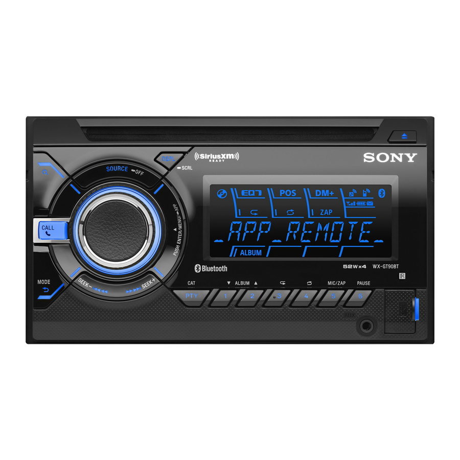
Photo: WX-GT90BT
Model Name Using Similar Mechanism
Mechanism Type
Optical Pick-up Name
SPECIFICATIONS
MW/LW
Tuning range:
MW: 531 – 1,602 kHz
LW: 153 – 279 kHz
Antenna (aerial) terminal:
External antenna (aerial) connector
Intermediate frequency:
9,124.5 kHz or 9,115.5 kHz/4.5 kHz
Sensitivity: MW: 26 μV, LW: 45 μV
Tuner section (Russian model)
FM
Tuning range:
FM1/FM2: 87.5 – 108.0 MHz (at 50 kHz step)
FM3: 65 – 74 MHz (at 30 kHz step)
Antenna (aerial) terminal:
External antenna (aerial) connector
Intermediate frequency: 25 kHz
Usable sensitivity: 8 dBf
Selectivity: 75 dB at 400 kHz
Signal-to-noise ratio: 80 dB (stereo)
Separation: 50 dB at 1 kHz
Frequency response: 20 – 15,000 Hz
MW/LW
Tuning range:
MW: 531 – 1,602 kHz
LW: 153 – 279 kHz
Antenna (aerial) terminal:
External antenna (aerial) connector
Intermediate frequency:
9,124.5 kHz or 9,115.5 kHz/4.5 kHz
Sensitivity: MW: 26 μV, LW: 45 μV
Tuner section (E and Indian models)
FM
Tuning range:
87.5 – 108.0 MHz (at 50 kHz step)
87.5 – 108.0 MHz (at 100 kHz step)
87.5 – 107.9 MHz (at 200 kHz step)
FM tuning step:
50 kHz/100 kHz/200 kHz switchable
Antenna (aerial) terminal:
External antenna (aerial) connector
Intermediate frequency: 25 kHz
Usable sensitivity: 8 dBf
Selectivity: 75 dB at 400 kHz
Signal-to-noise ratio: 80 dB (stereo)
Separation: 50 dB at 1 kHz
Frequency response: 20 – 15,000 Hz
WX-GT90BT/GT90BTE/
AM
Tuning range:
531 – 1,602 kHz (at 9 kHz step)
530 – 1,710 kHz (at 10 kHz step)
AM tuning step: 9 kHz/10 kHz switchable
Antenna (aerial) terminal:
External antenna (aerial) connector
Intermediate frequency:
9,124.5 kHz or 9,115.5 kHz/4.5 kHz
(at 9 kHz step)
9,115 kHz or 9,125 kHz/5 kHz
(at 10 kHz step)
Sensitivity: 26 μV
CD Player section
Signal-to-noise ratio: 120 dB
Frequency response: 10 – 20,000 Hz
Wow and flutter: Below measurable limit
USB Player section
Interface: USB (Full-speed)
Maximum current: 1 A
Wireless Communication
Communication System:
Bluetooth Standard version 2.1 + EDR
Output:
Bluetooth Standard Power Class 2
(Max. +4 dBm)
Maximum communication range:
Line of sight approx. 10 m (33 ft)*
1
Frequency band:
2.4 GHz band (2.4000 – 2.4835 GHz)
Modulation method: FHSS
2
Compatible Bluetooth Profiles*
:
A2DP (Advanced Audio Distribution Profile)
1.2
AVRCP (Audio Video Remote Control Profile)
1.3
HFP (Handsfree Profile) 1.5
PBAP (Phone Book Access Profile)
SPP (Serial Port Profile)
GT99BT
US Model
Canadian Model
AEP Model
UK Model
E Model
WX-GT90BT
Russian Model
WX-GT90BTE
Indian Model
WX-GT99BT
MEX-BT4100U/
WX-GT80UE/GT80UI/GT88UI
MG-101CA-188
DAX-25A
*1 The actual range will vary depending on
factors such as obstacles between devices,
magnetic fields around a microwave oven,
static electricity, reception sensitivity, antenna
(aerial)'s performance, operating system,
software application, etc.
*2 Bluetooth standard profiles indicate the
purpose of Bluetooth communication
between devices.
Power amplifier section
Output: Speaker outputs
Speaker impedance: 4 – 8 ohms
Maximum power output: 52 W × 4 (at 4 ohms)
General
Outputs:
Audio outputs terminal (front, rear, sub)
Power antenna (aerial)/Power amplifier control
terminal (REM OUT)
Inputs:
SiriusXM input terminal
(US and Canadian models only)
Remote controller input terminal
Antenna (aerial) input terminal
MIC input terminal
AUX input jack (stereo mini jack)
USB port
Power requirements: 12 V DC car battery
(negative ground (earth))
Dimensions: Approx. 178 × 100 × 178 mm
1
× 4 × 7
1
(7
/
/
in) (w/h/d)
8
8
Mounting dimensions: Approx. 182 × 111 × 159
1
× 4
3
× 6
3
mm (7
/
/
/
in) (w/h/d)
4
8
8
Mass: Approx. 1.4 kg (3 lb 2 oz)
Supplied accessories:
Remote commander: RM-X231
Microphone
Parts for installation and connections (1 set)
Design and specifications are subject to change
without notice.
AUDIO SYSTEM
Advertisement
Table of Contents

Related Manuals for Sony WX-GT90BT


Summary of Contents for Sony WX-GT90BT
-
Page 1: Specifications
Frequency response: 20 – 15,000 Hz Selectivity: 75 dB at 400 kHz Signal-to-noise ratio: 80 dB (stereo) Separation: 50 dB at 1 kHz Frequency response: 20 – 15,000 Hz 9-893-631-01 Sony Corporation 2012L33-1 © 2012.12 Published by Sony Techno Create Corporation... -
Page 2: Flexible Circuit Board Repairing
Do not touch the soldering iron on the same conductor of the TIONNEMENT. NE REMPLACER CES COMPOSANTS QUE circuit board (within 3 times). PAR DES PIÈCES SONY DONT LES NUMÉROS SONT DON- • Be careful not to apply force on the conductor when soldering NÉS DANS CE MANUEL OU DANS LES SUPPLÉMENTS... -
Page 3: Table Of Contents
WX-GT90BT/GT90BTE/GT99BT SECTION 1 SERVICING NOTES TABLE OF CONTENTS NOTES ON HANDLING THE OPTICAL PICK-UP BLOCK OR BASE UNIT SERVICING NOTES ..........The laser diode in the optical pick-up block may suffer electro- GENERAL static break-down because of the potential difference generated by .............. - Page 4 WX-GT90BT/GT90BTE/GT99BT NOTE THE MAIN BOARD OR SYSTEM CONTROLLER 2-2. Display in Destination Setting Mode (IC501) REPLACING (Displayed characters/values in the following fi gure are example) When the MAIN board or system controller (IC501) is replaced, Destination code the destination setting is necessary.
- Page 5 WX-GT90BT/GT90BTE/GT99BT 2-4. Destination Code TEST DISCS Use following TEST DISC (for CD) when this set confi rms the Model Destination OP5 OP4 OP3 OP2 OP1 OP0 operation and checks it. US, Canadian WX-GT90BT AEP, UK Part No. Description WX-GT90BTE Russian...
- Page 6 WX-GT90BT/GT90BTE/GT99BT NOTE FOR REPLACEMENT OF THE USB CONNEC- REPLACING THE LITHIUM BATTERY TOR (CN971) AND THE AUX JACK (J901) OF THE REMOTE COMMANDER To replace the USB connector and AUX jack requires alignment. When the battery becomes weak, the range 1.
- Page 7 WX-GT90BT/GT90BTE/GT99BT EXTENSION CABLE AND SERVICE POSITION When repairing or servicing this set, connect the jig cable (extension cable (CD mecha)) as shown below. • Connect the MAIN board (CN700) and the SERVO board (CN401) with the jig cable. Jig cable: Part No.
- Page 8 90BTE/GT99BT, the track information won’t be shown. Approx. 80 cm Even if there is no track information on display during playback of an AVRCP1.3 device, it is not a failure of WX-GT90BT/GT- 90BTE/GT99BT. 1. Connect the Bluetooth audio device (or cellular phone with Bluetooth audio function) with this unit, and confi...
-
Page 9: General
WX-GT90BT/GT90BTE/GT99BT SECTION 2 This section is extracted GENERAL from instruction manual. (US and Canadian models) Equipment used in illustrations (not supplied) Appareils utilisés dans les illustrations (non fournis) Front speaker Subwoofer Power amplifier Rear speaker Haut-parleur avant Caisson de graves Amplificateur de puissance Haut-parleur arrière... - Page 10 You may not be able to install this unit in some makes of températures extrêmement élevées. it and other parts from obstructing your driving. Japanese cars. In such a case, consult your Sony dealer. -B Montage de l’appareil dans une Il est extrêmement dangereux que le cordon s'enroule...
- Page 11 WX-GT90BT/GT90BTE/GT99BT (AEP, Russian and UK models) Depending on the type of car, use an adaptor (not Abhängig vom Autotyp müssen Sie einen Adapter Selon le type de voiture, utilisez un adaptateur (non In base al tipo di automobile, utilizzare un adattatore Afhankelijk van het soort wagen gebruikt u een supplied) if the antenna connector does not fit.
- Page 12 Install clips (not supplied) and adjust the length unbedingt darauf, dass das Kabel und andere Teile beim revendeur de l’appareil ou votre concessionnaire avant Japanese cars. In such a case, consult your Sony dealer. and position of the cord so that it does not japanischen Fahrzeug ( Fahren nicht hinderlich sind.
-
Page 13: Connection Diagram
WX-GT90BT/GT90BTE/GT99BT (E and Indian models) Equipment used in illustrations (not supplied) Equipo utilizado en las ilustraciones (no suministrado) Front speaker Subwoofer Power amplifier Rear speaker Altavoz frontal Altavoz potenciador Amplificador de potencia Altavoz posterior de graves Fuse (10 A) Fusible (10 A) Speaker impedance: 4 –... - Page 14 Es posible que no pueda instalar esta unidad en algunos Precauciones Choose the installation location carefully so that the unit Japanese cars. In such a case, consult your Sony dealer. to install the microphone (supplied). Elija cuidadosamente el lugar de montaje de forma que automóviles japoneses.
-
Page 15: Disassembly
WX-GT90BT/GT90BTE/GT99BT SECTION 3 DISASSEMBLY • This set can be disassembled in the order shown below. 3-1. DISASSEMBLY FLOW 3-2. MINI FUSE (BLADE TYPE) (10A/32V) (FU1), 3-15. KNOB COVER (Page 23) (Page 16) 3-3. FRONT PANEL BLOCK (Page 16) 3-4. CD MECHANISM DECK (MG-101CA-188) (Page 17) 3-7. -
Page 16: Mini Fuse (Blade Type) (10A/32V) (Fu1), Cover
WX-GT90BT/GT90BTE/GT99BT Note: Follow the disassembly procedure in the numerical order given. 3-2. MINI FUSE (BLADE TYPE) (10A/32V) (FU1), COVER 4 cover 2 two bosses 3 three claws 1 mini fuse (blade type) (10A/32V) (FU1) 3-3. FRONT PANEL BLOCK 4 connector... -
Page 17: Cd Mechanism Deck (Mg-101Ca-188)
WX-GT90BT/GT90BTE/GT99BT 3-4. CD MECHANISM DECK (MG-101CA-188) 6 CD mechanism deck 4 two screws (MG-101CA-188) (PTT2.6 5 bracket (CD) 1 screw (PTT2.6 2 Lift up the CD mechanism block . 3 connector (CN700) 1 screw 1 two screws (PTT2.6 (PTT2.6 3-5. -
Page 18: Main Board (With Bt Board)
WX-GT90BT/GT90BTE/GT99BT 3-6. MAIN BOARD (WITH BT BOARD) Note: When the complete MAIN board is replaced, the destination setting is necessary. Refer to “NOTE THE MAIN BOARD OR SYSTEM CONTROLLER (IC501) REPLACING” on page 4. 2 screw 1 three ground point screws (PTT2.6... -
Page 19: Chassis (T) Sub Assy
WX-GT90BT/GT90BTE/GT99BT 3-8. CHASSIS (T) SUB ASSY 1 two screws (M1.7 2.5) 1 two screws (M1.7 2.5) 3 chassis (T) sub assy 2 claw 3-9. ROLLER ARM ASSY 5 roller arm assy 4 gear (HRA) 1 spring (RAL) 3 washer 2 spring (RAR) -
Page 20: Chassis (Op) Assy
WX-GT90BT/GT90BTE/GT99BT 3-10. CHASSIS (OP) ASSY 8 chassis (OP) assy 1 tension spring (KF) 6 two coil springs (damper) (natural) 7 coil spring (damper) (blue) 4 slider (R) 3 lever (D) 2 gear (LE1) 3-11. CHUCKING ARM SUB ASSY 3 chucking arm sub assy 1 spring Note 1: Have this portion receive the chassis. -
Page 21: Sled Motor Assy
WX-GT90BT/GT90BTE/GT99BT 3-12. SLED MOTOR ASSY 2 three serration screws 3 sled motor assy 1 spring turn table spring stand Note 2: Never remove these parts since they were adjusted. bearing (F) – – stand Note 1: Place the stand with care not to touch the turn table. -
Page 22: Optical Pick-Up Section
WX-GT90BT/GT90BTE/GT99BT 3-13. OPTICAL PICK-UP SECTION 2 optical pick-up section Note: Be careful not to touch the lens and hologram terminal when removing the optical pick-up section. – bottom side view – 3-14. OPTICAL PICK-UP 1 tapping screw (P 1.4) 2 leaf spring (OPS) -
Page 23: Knob
WX-GT90BT/GT90BTE/GT99BT 3-15. KNOB 1 Remove the knob block in the direction of an arrow. 6 light guide (ring) 7 knob 4 two claws 2 spring (VOL) 3 rubber (knob) 4 two claws 5 knob (top) 1 Align four holes. 2 Insert in four claws of knob (top). -
Page 24: Test Mode
WX-GT90BT/GT90BTE/GT99BT SECTION 4 TEST MODE SETTING THE TEST MODE Setting method: 1. Press the [ OFF SOURCE] button for 1 second to turn the power off. 2. Press the [ 4] t [MIC/ZAP 5] t [ V ALBUM 1] buttons sequentially (the [ V ALBUM 1] button is pressed for two sec- onds). -
Page 25: Diagrams
WX-GT90BT/GT90BTE/GT99BT SECTION 5 DIAGRAMS 5-1. BLOCK DIAGRAM - SERVO Section - CD MECHANISM DECK BLOCK (MG-101CA-188) FL, RL, SUB (Page 26) FPI1 DAO3 (F_L-CH) FPI2 DAO2 (F_R-CH) R-CH FNI1 FNI2 DAO4 (R_L-CH) DAO1 (R_R-CH) R-CH CD HEAD AMP, DAO5 (SUB-CH) -
Page 26: Block Diagram - Main Section
WX-GT90BT/GT90BTE/GT99BT 5-2. BLOCK DIAGRAM - MAIN Section - (US, Canadian, AEP, Russian, UK) (E, Indian) ELECTRICAL VOLUME, INPUT SELECTOR LINE AMP IC401 IC404 J403 FL, RL, SUB (Page 25) 33 AU_IN_FL AU_OUT_FL 36 2 IN_FL OUT2 31 FRONT AUDIO OUT... -
Page 27: Block Diagram - Panel/Power Supply Section
WX-GT90BT/GT90BTE/GT99BT 5-3. BLOCK DIAGRAM - PANEL/POWER SUPPLY Section - MAIN SYSTEM CONTROLLER IC501 (3/3) XOUT X502 32.768kHz OSCOUT +1.5V IC701 VDD +1.5V X501 REGULATOR IC681 7.92MHz OSCIN DSP_1_5V 65 +1.5V IC701 VDDM +1.5V REGULATOR IC682 +3.3V REGULATOR BU +3.3V REGULATOR... - Page 28 WX-GT90BT/GT90BTE/GT99BT THIS NOTE IS COMMON FOR PRINTED WIRING BOARDS AND SCHEMATIC DIAGRAMS. • Waveforms (In addition to this, the necessary note is printed in each block.) – MAIN Board – For Printed Wiring Boards. For Schematic Diagrams. IC1300 1 (BST)
-
Page 29: Schematic Diagram - Main Section (1/5)
WX-GT90BT/GT90BTE/GT99BT 5-4. SCHEMATIC DIAGRAM - MAIN Section (1/5) - • See page 39 for IC Block Diagrams. MAIN BOARD (1/5) IC301 IC B/D (US, CND, E, IND) POWER AMP, REGULATOR CN301 IC301 REAR RCH (+) TDF8556AJ/N5 REAR LCH (+) C367 REAR RCH (–) -
Page 30: Schematic Diagram - Main Section (2/5)
WX-GT90BT/GT90BTE/GT99BT 5-5. SCHEMATIC DIAGRAM - MAIN Section (2/5) - • See page 39 for IC Block Diagrams. MAIN BOARD (2/5) Q407 13.8 LTA014EUBFS8TL R427 13.8 Q407 - 409 MUTING CONTROL R425 R470 MAIN BOARD (1/5) J403 R468 (Page 29) R412... -
Page 31: Schematic Diagram - Main Section (3/5)
WX-GT90BT/GT90BTE/GT99BT 5-6. SCHEMATIC DIAGRAM - MAIN Section (3/5) - • See page 28 for Waveforms. • See page 39 for IC Block Diagrams. • See page 43 for IC Pin Function Description. MAIN BOARD (3/5) MAIN BOARD (1/5) BU_IN (Page 29) -
Page 32: Schematic Diagram - Main Section (4/5)
WX-GT90BT/GT90BTE/GT99BT 5-7. SCHEMATIC DIAGRAM - MAIN Section (4/5) - • See page 28 for Waveforms. • See page 39 for IC Block Diagrams. • See page 43 for IC Pin Function Description. MAIN BOARD (4/5) JL730 C787 C779 C776 C789 0.01... -
Page 33: Schematic Diagram - Main Section (5/5)
WX-GT90BT/GT90BTE/GT99BT 5-8. SCHEMATIC DIAGRAM - MAIN Section (5/5) - • See page 28 for Waveforms. • See page 39 for IC Block Diagrams. • See page 43 for IC Pin Function Description. MAIN BOARD (5/5) JL611 JL612 JL609 JL608 JL613... -
Page 34: Printed Wiring Board - Main Section (1/2)
WX-GT90BT/GT90BTE/GT99BT 5-9. PRINTED WIRING BOARD - MAIN Section (1/2) - • : Uses unleaded solder. MAIN BOARD (COMPONENT SIDE) (US, CND) C876 R857 R855 C830 IC830 C457 C878 (AEP, UK) R308 C877 IC831 R873 C357 R831 D306 R874 C314 FB306... -
Page 35: Printed Wiring Boards - Main Section (2/2)
WX-GT90BT/GT90BTE/GT99BT 5-10. PRINTED WIRING BOARDS - MAIN Section (2/2) - • : Uses unleaded solder. CN301 (US, CND) J403 (FRONT VIEW) (US, CND, E, IND) REAR FRONT J801 AUDIO OUT AUDIO OUT REMOTE REAR LCH (+) REAR RCH (+) MAIN BOARD... -
Page 36: Key Board (Component Side)
WX-GT90BT/GT90BTE/GT99BT 5-11. PRINTED WIRING BOARD - KEY Board (Component Side) - • : Uses unleaded solder. S951 KEY BOARD (COMPONENT SIDE) S952 SOURCE S956 S966 DSPL SCRL LED901, 902 (RING ILLUMINATION) LED904 LED900 LED902 LED901 S957 LCD901 CALL LIQUID CRYSTAL DISPLAY... -
Page 37: Printed Wiring Board - Key Board (Conductor Side)
WX-GT90BT/GT90BTE/GT99BT 5-12. PRINTED WIRING BOARD - KEY Board (Conductor Side) - • : Uses unleaded solder. KEY BOARD (CONDUCTOR SIDE) (Page 35) MAIN BOARD CN102 R949 R941 R942 R933 R934 Q905 R927 R926 R974 R931 R980 R938 Q900 R932 Q901... -
Page 38: Schematic Diagram - Key Board
WX-GT90BT/GT90BTE/GT99BT 5-13. SCHEMATIC DIAGRAM - KEY Board - • See page 39 for IC Block Diagrams. KEY BOARD IC902 R907 R909 R910 R911 R914 R916 R900 R903 R905 REMOTE CONTROL RECEIVER IC902 PNJ4813M01S0 R908 R901 LED902 LED900 R975 R974 SMLVN6RGB1U1... -
Page 39: Ic Block Diagrams
WX-GT90BT/GT90BTE/GT99BT • IC Block Diagrams – MAIN Board – IC301 TDF8556AJ/N5 I2C_SIO OUT-FL– C BUS I2C_SCK OUT-FL+ OUT-RL– P-GND1 OUT-RL+ IN-RL IN-FL S-GND PROTECTION/ DIAGNOSTIC IN-FR IN-RR BEEP OUT-RR+ P-GND3 OUT-RR– OUT-FR+ STANDBY/ MUTE OUT-FR– CHIP DETECT/ P-GND4 DIAGNOSTIC TEMPERATURE... - Page 40 WX-GT90BT/GT90BTE/GT99BT IC401 BD3467FV-E2 FADER FADER BOOST OUTC FADER FADER A1 1 BOOST OUTS A2 2 FADER FADER B1 3 OUTR1 BOOST B2 4 FADER FADER OUTR2 BOOST CP1 5 FADER FADER CN 6 OUTF1 BOOST CP2 7 FADER FADER OUTF2...
- Page 41 WX-GT90BT/GT90BTE/GT99BT IC404 NJW1240V (TE2) MUTING OUT1 IN1 1 MUTING OUT2 IN2 2 MUTING OUT3 IN3 3 MUTING OUT4 IN4 4 MUTING OUT5 IN5 5 MUTING OUT6 IN6 6 POP NOISE MUTE 7 SUPPRESSION GAIN SELECT GAIN 8 6 dB/8 dB...
- Page 42 WX-GT90BT/GT90BTE/GT99BT IC1300 OZ539IGN-A1-0-TR BST 1 VREF OSCILLATOR LX 2 REFERENCE GENERATOR OVER CURRENT PROTECTION GNDA VIN 3 EN_SYS 4 USBOUT 5 FB_USB 6 SS_SYS ADJUSTMENT GENERATOR CHARGE EN_USB PUMP VIC_USB USBIN OVER-CURRENT ISET_USB LIMIT VOUT_SYS (USBIN) UVLS FAULT PROTECTION –...
- Page 43 WX-GT90BT/GT90BTE/GT99BT • IC Pin Function Description MAIN BOARD IC501 R5F3650ECDZ98FB (MAIN SYSTEM CONTROLLER) (AEP, Russian, UK, E and Indian models) IC501 R5F3650KCDZ95FB (MAIN SYSTEM CONTROLLER) (US and Canadian models) Pin No. Pin Name Description NOSE_SW Front panel remove/attach detection signal input terminal Fixed at “L”...
- Page 44 WX-GT90BT/GT90BTE/GT99BT Pin No. Pin Name Description AMPSTB Standby control signal output to the power amplifi er GHOST_RST Reset signal output to the sub system controller “L”: reset VCC2 Power supply terminal (+3.3V) GHOST_1_5V Not used Ground terminal DSP_RST Reset signal output to the audio DSP “L”: reset...
- Page 45 WX-GT90BT/GT90BTE/GT99BT MAIN BOARD IC601 TMPM320C1DFG-9999 (SUB SYSTEM CONTROLLER) Pin No. Pin Name Description MODE1 Operation mode setting terminal Fixed at “L” in this unit RESETn Reset signal input terminal from the main system controller DRV_ON Driver control signal output to the CD section...
- Page 46 WX-GT90BT/GT90BTE/GT99BT Pin No. Pin Name Description I2C_SDA Two-way data bus with the EEPROM DVCC1.2 Power supply terminal (+1.2V) 63 to 68 D0 to D5 Two-way data bus terminal Not used DVSSCOM Ground terminal Two-way data bus terminal Not used DVCC3.3IO Power supply terminal (+3.3V)
- Page 47 WX-GT90BT/GT90BTE/GT99BT MAIN BOARD IC701 TC94A99FG-003 (SY, H (CD HEAD AMP, DIGITAL SERVO PROCESSOR, AUDIO DSP) Pin No. Pin Name Description LPFO Signal output from the operation amplifi er for PLL loop fi lter PVREF Reference voltage (+1.65V) input terminal VCOF Terminal for VCO fi...
- Page 48 WX-GT90BT/GT90BTE/GT99BT Pin No. Pin Name Description ADVDD3 Power supply terminal (+3.3V) ADIN1 (IN_L-CH) Audio signal input terminal (L channel) ADVREFL Reference voltage output terminal ADVCM Reference voltage output terminal ADVREFH Reference voltage output terminal ADIN2 (IN_R-CH) Audio signal input terminal (R channel)
-
Page 49: Exploded Views
WX-GT90BT/GT90BTE/GT99BT SECTION 6 EXPLODED VIEWS Note: • -XX and -X mean standardized parts, so • Color Indication of Appearance Parts Ex- The components identifi ed by mark 0 they may have some difference from the ample: or dotted line with mark 0 are critical for original one. -
Page 50: Front Panel Section
WX-GT90BT/GT90BTE/GT99BT 6-2. FRONT PANEL SECTION KEY board RE901 not supplied CCB1 LCD901 IC902 CN971 J901 not supplied not supplied not supplied Note: Refer to the servicing notes “NOTE FOR REPLACEMENT OF THE USB CONNECTOR (CN971) AND THE AUX JACK (J901)” on page 6, if replacing CN971 and J901. -
Page 51: Cd Mechanism Deck Section (Mg-101Ca-188)
WX-GT90BT/GT90BTE/GT99BT 6-3. CD MECHANISM DECK SECTION (MG-101CA-188) CDM1 DAX1 not supplied supplied not supplied not supplied not supplied not supplied not supplied SENSOR board not supplied not supplied not supplied not supplied not supplied Ref. No. Part No. Description Remark Ref. -
Page 52: Electrical Parts List
WX-GT90BT/GT90BTE/GT99BT SECTION 7 ELECTRICAL PARTS LIST Note: • Due to standardization, replacements in • CAPACITORS When indicating parts by reference num- the parts list may be different from the uF: μF ber, please include the board name. parts specifi ed in the diagrams or the com- •... - Page 53 WX-GT90BT/GT90BTE/GT99BT MAIN Ref. No. Part No. Description Remark Ref. No. Part No. Description Remark R926 1-216-833-11 METAL CHIP 1/10W S957 1-798-448-11 TACTILE SWITCH (CALL, R927 1-216-833-11 METAL CHIP 1/10W S959 1-798-448-11 TACTILE SWITCH (PAUSE, 6) R928 1-216-833-11 METAL CHIP 1/10W...
- Page 54 WX-GT90BT/GT90BTE/GT99BT MAIN Ref. No. Part No. Description Remark Ref. No. Part No. Description Remark C353 1-164-866-11 CERAMIC CHIP 47PF C466 1-165-908-11 CERAMIC CHIP 1uF C354 1-164-866-11 CERAMIC CHIP 47PF (E, IND) C467 1-165-908-11 CERAMIC CHIP 1uF C355 1-164-866-11 CERAMIC CHIP 47PF...
- Page 55 WX-GT90BT/GT90BTE/GT99BT MAIN Ref. No. Part No. Description Remark Ref. No. Part No. Description Remark C689 1-165-884-91 CERAMIC CHIP 2.2uF 6.3V C784 1-164-245-11 CERAMIC CHIP 0.015uF C690 1-112-717-91 CERAMIC CHIP 1uF 6.3V C786 1-114-582-91 CERAMIC CHIP 0.1uF C701 1-100-597-91 CERAMIC CHIP 0.1uF...
- Page 56 WX-GT90BT/GT90BTE/GT99BT MAIN Ref. No. Part No. Description Remark Ref. No. Part No. Description Remark D530 6-503-759-01 DIODE RB751V40, 115 IC681 6-716-355-01 IC BU15TD3WG-TR D602 6-503-759-01 DIODE RB751V40, 115 D805 6-503-206-01 DIODE RKZ7.5B2KGP1 IC682 6-716-355-01 IC BU15TD3WG-TR IC701 6-715-712-11 IC TC94A99FG-003 (SY, H...
- Page 57 WX-GT90BT/GT90BTE/GT99BT MAIN Ref. No. Part No. Description Remark Ref. No. Part No. Description Remark R304 1-216-214-00 METAL CHIP 4.7K 1/8W R426 1-216-296-11 SHORT CHIP (E, IND) R427 1-218-990-81 SHORT CHIP R305 1-216-182-00 METAL CHIP 1/8W R429 1-218-933-11 METAL CHIP 1/16W...
- Page 58 WX-GT90BT/GT90BTE/GT99BT MAIN Ref. No. Part No. Description Remark Ref. No. Part No. Description Remark R535 1-218-953-11 METAL CHIP 1/16W R638 1-218-977-11 METAL CHIP 100K 1/16W R536 1-218-977-11 METAL CHIP 100K 1/16W R639 1-218-977-11 METAL CHIP 100K 1/16W R540 1-218-977-11 METAL CHIP...
- Page 59 WX-GT90BT/GT90BTE/GT99BT MAIN SENSOR SERVO Ref. No. Part No. Description Remark Ref. No. Part No. Description Remark R819 1-218-953-11 METAL CHIP 1/16W A-1866-089-A SERVO BOARD, COMPLETE R820 1-218-953-11 METAL CHIP 1/16W ********************** R830 1-218-972-11 METAL CHIP 1/16W (US, CND) When the SERVO board is defective, exchange the complete mounted board.
- Page 60 WX-GT90BT/GT90BTE/GT99BT Ref. No. Part No. Description Remark PARTS FOR INSTALLATION AND CONNECTIONS ************************************** X-2514-519-3 FRAME, FITTING ASSY (AEP, RU, UK, E, IND) 3-876-675-01 KEY (FRAME) (1 piece) (AEP, RU, UK, E, IND) 1-846-033-11 CONNECTION CABLE (ISO) (POWER) (AEP, RU, UK)
- Page 61 WX-GT90BT/GT90BTE/GT99BT MEMO...
-
Page 62: Revision History
WX-GT90BT/GT90BTE/GT99BT REVISION HISTORY Checking the version allows you to jump to the revised page. Also, clicking the version at the top of the revised page allows you to jump to the next revised page. Ver. Date Description of Revision 2012.12...