Chapters
Table of Contents
Troubleshooting

Related Manuals for LG RCT689H


Summary of Contents for LG RCT689H
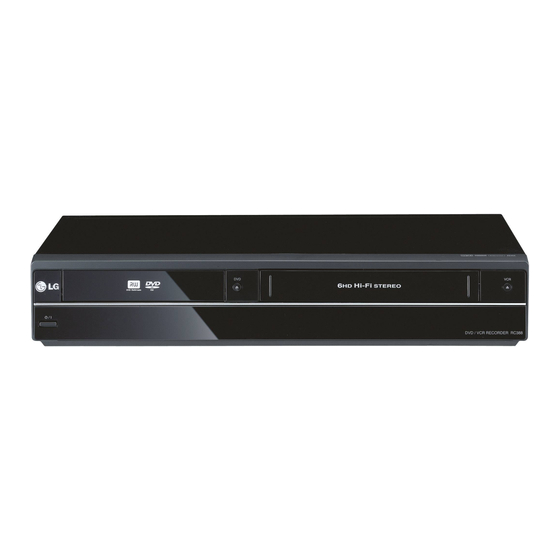
- Page 1 Internal Use Only Website http://biz.lgservice.com VCR+DVD RECORDER SERVICE MANUAL MODEL: RCT689H CAUTION BEFORE SERVICING THE UNIT, READ THE “SAFETY PRECAUTIONS” IN THIS MANUAL. FEBRUARY, 2011 P/NO : AFN32896765...
- Page 2 CONTENTS SECTION 1 ..SUMMARY SECTION 2 ..CABINET & MAIN CHASSIS SECTION 3 ..ELECTRICAL SECTION 4 ..MECHANISM OF VCR PART(D-37) SECTION 5 ..RV9 LOADER PART SECTION 6 ..REPLACEMENT PARTS LIST...
- Page 3 SECTION 1 SUMMARY CONTENTS PRODUCT SAFETY SERVICING GUIDELINES FOR VCR+DVD RECORDER PRODUCTS ....................1-3 SERVICING PRECAUTIONS ........................1-4 • General Servicing Precautions • Insulation Checking Prodedure • Electrostatically Sensitive Devices SERVICE INFORMATION FOR EEPROM IC SETTING ..............1-5 UPGRADE THE MAIN & LOADER PROGRAM ................
- Page 4 When servicing this product, under no circumstances should the original design be modified or altered without permission from LG Corporation. All components should be replaced only with types identical to those in the original circuit and their physical location, wiring and lead dress must conform to original layout upon completion of repairs.
-
Page 5: Servicing Precautions
SERVICING PRECAUTIONS CAUTION: Before servicing the VCR+DVD RECORDER Electrostatically Sensitive (ES) Devices covered by this service data and its supplements and Some semiconductor (solid state) devices can be damaged addends, read and follow the SAFETY PRECAUTIONS. easily by static electricity. Such components commonly are NOTE: if unforeseen circumstances create conflict between called Electrostatically Sensitive (ES) Devices. -
Page 6: Service Information For Eeprom Ic Setting
SERVICE INFORMATION FOR EEPROM IC SETTING 1. Press both “CLEAR” button on the Remocon and “ OPEN/CLOSE” button on the Front Panel about ±5 sec. The picture on OSD will be as bellow : OP1 : 0F 00000000 OP2 : 70 00000000 071102A OP3 : 31... - Page 7 UPGRADE THE MAIN & LOADER PROGRAM 1. MAKING UPGRADE DISC MAIN SW AND 5) Press “PLAY” button to update S/W and another button to cancel. LOADER SW 6) Main S/W under updated. 1) Do Physical format as ISO9660 or JOLIET file Do not turn off the power during updating proc- system ess...!
- Page 8 5) Press “PLAY” button to update S/W and another 3) Select menu button to cancel. 'General -> TV Aspect -> 16:9 Wide' 6) Loader S/W under updated. Do not turn off the power during updating proc- ess...! If updating succeed, after completed there will be message : 4) Press button number 1 - 3 -9 - 7 - 1 - 3 - 9 - Enter on the Remocon...
- Page 9 UPGRADING I/O μ-com SOFTWARE 1. MAKING UPGRADE CD 1) Prepare “io_micom_update.hex” File. 2) Make Data CD with Your Burning Tool. 2. UPGRADING SEQUENCE 1) Insert Your Upgrading CD. 2) There will be displayed Update Disc OSD and Request Pressing Play Key. Then Press Play Key! --->...
-
Page 10: Specifications
SPECIFICATIONS • GENERAL Power requirements AC 200 ~ 240V, 50/60Hz Power consumption Dimensions (approx.) 430 X 78.5 X 260mm (w x h x d) without foot Net weight (approx.) 4.2kg Operating temperature 5°C to 35°C Operating humidity 5% to 90 % Television system PAL B/G, SECAM D/K, color system Recording format... - Page 11 MEMO 1-10...
-
Page 12: Table Of Contents
SECTION 2 CABINET & MAIN CHASSIS CONTENTS EXPLODED VIEWS ............................. 2-2 1. CABINET AND MAIN FRAME SECTION ....................2-2 2. DECK MECHANISM SECTION [RV9(DR-11A)] ..................2-3 3. DECK MECHANISM SECTION (D37(N)) ....................2-4 4. PACKING ACCESSORY SECTION ......................2-7... -
Page 13: Exploded Views
EXPLODED VIEWS 1. CABINET AND MAIN FRAME SECTION... -
Page 14: Deck Mechanism Section [Rv9(Dr-11A)]
2. DECK MECHANISM SECTION [RV9(DR-11A)] 1431 1001 1003 1002 A001 1030 1437 1025 A006 1038 1041 1432 1432 1026 1017 1036 1041 1433 1013 1011 1016 1432 1020 1015 1012 CABLE5 DVD & LOADER BOARD CABLE6 1043 1046 1047 1439... -
Page 15: Deck Mechanism Section (D37(N))
3. DECK MECHANISM SECTION (D37(N)) 3-1. Front loading mechanism section... - Page 16 3-2. Moving mechanism section (1) OPTIONAL PART...
- Page 17 3-3. Moving mechanism section (2)
-
Page 18: Packing Accessory Section
4. PACKING ACCESSORY SECTION 806 CABLE(COAXIAL) BATTERY REMOCON 801 INSTRUCTION ASSEMBLY PACKING PACKING BOX CARTON... - Page 19 MEMO...
- Page 20 SECTION 3 ELECTRICAL CONTENTS OVERALL WIRING DIAGRAM 1. VCR P.C.BOARD ........3-61 ....3-2 2. SMPS P.C.BOARD ........3-65 3. HDMI P.C.BOARD ........3-65 VCR PART 4. KEY P.C.BOARD ........3-67 ELECTRICAL VDR PART ADJUSTMENT PROCEDURES ....3-3 1. SERVO ADJUSTMENT .......3-3 VDR ELECTRICAL VCR ELECTRICAL TROUBLESHOOTING GUIDE ....3-71 TROUBLESHOOTING GUIDE...
-
Page 21: Overall Wiring Diagram
OVERALL WIRING DIAGRAM PVM01 PV601 PHM01 P6V01 PMH01 PMS01 TS_CLK TS_SYNC TS_DATA TS_VALID /DEMOD_RST TU_PWR_CTL ERROR USB_PO USB_OC USB_BDMO USB_BDPO TPB- TPB+ TPA- TPA+ /DVD_RST SYNC_DET_H /VDEC_RST /SPI_CS1 VI-DO VI_D1 VI_D2 VI_D3 VI_D4 VI_D5 VI_D6 VI_D7 VI_CLK AI_MCLK AI_SCLK AI_FSYNC AI_DO AO_MCLK SPDIF... -
Page 22: Vcr Part
VCR PART ELECTRICAL ADJUSTMENT PROCEDURES 1. SERVO ADJUSTMENT 1) PG Adjustment • Test Equipment a) OSCILLOSCOPE b) PAL MODEL : PAL SP TEST TAPE • Adjustment And Specification MODE MEASUREMENT POINT ADJUSTMENT POINT SPECIFICATION V.Out 6.5 ± 0.5H PLAY R/C TRK JIG KEY H/SW(TP) •... -
Page 23: Vcr Electrical Troubleshooting Guide
VCR ELECTRICAL TROUBLESHOOTING GUIDE 1. POWER (SMPS) CIRCUIT No .5.3VA Is the F101 normal? Replace the F101 (Use the same Fuse) Is the BD101 normal? Replace the BD101 Is the R101 normal? Replace the R101 Is Vcc (13V - 27V) Is the D102 normal? supplied to IC101 Pin2? Check or Replace the D102... -
Page 24: Vcr Main
VCR ELECTRICAL TROUBLESHOOTING GUIDE VCR MAIN No 5.0V Is the Check or Replace the D123 Vcc(5.3V) supplied to Q801 collector? Check the 33V Line or ZD815 Is the Q801 Base “H”? Check or Replace the Q801 No REG 12V Is the Check or Replace the D122 Vcc(13V) supplied to Q802 collector? - Page 25 VCR ELECTRICAL TROUBLESHOOTING GUIDE No Cap Vcc or 13.5VA Is the D122 normal? Replace the D122 Power Line of Main PCB is short No 3.3V Is the Vcc(3.8V) supplied to Check or Replace the D127 IC153 pin1? Check the DVD CTL Is the IC153 pin4 “H”? “H”...
- Page 26 VCR ELECTRICAL TROUBLESHOOTING GUIDE No 2.5V Is the Vcc(13.5V) supplied to D156 Check or Replace the D156 anode? Check the DVD CTL Is the IC154 pin4 “H”? “H” signal from IO u-COM(IC601 #29) Check or Replace the IC154 No 5VL Is the Vcc(5.5V) supplied to IC156 Check or Replace the D128...
-
Page 27: System/Key Circuit
VCR ELECTRICAL TROUBLESHOOTING GUIDE 2. SYSTEM/KEY CIRCUIT 2-1. AUTO STOP Auto Stop Does Check the Drum the H/SW waveform Motor signal. appear at IC501 Pin23? Do the Does 5.0V T/UP Reel Pulses T-UP Reel Pulses appear at the RS501? appear at the Q501 Base appear at IC501 terminal? Pin3? -
Page 28: Servo Circuit
VCR ELECTRICAL TROUBLESHOOTING GUIDE 3. SERVO CIRCUIT 3-1. Unstable Video in PB MODE Does the Noise level of the screen change periodically? Do the Is adjusting the height of Readjust the height of the CTL pulses appear at the CTL Head accurate? CTL Head. - Page 29 VCR ELECTRICAL TROUBLESHOOTING GUIDE 3-3. When the Capstan Motor doesn’t run, When the Capstan Motor doesn’t run, Does Refer to “SMPS(CAPSTAN/13.5VA) 12.5VA appear at PCM01 Trouble Shooting”. Pin2? Does 2.8V appear at PCM01 Pin9? Check the PMC01 and the Capstan Motor Ass’y. Does the PWM signal appear at IC501 Pin33?
-
Page 30: Y/C Circuit
VCR ELECTRICAL TROUBLESHOOTING GUIDE 4. Y/C CIRCUIT 4-1. When the Y(Luminance) signal doesn’t appear on the screen in PB Mode, When the Y(Luminance) signal doesn’t appear on the screen in PB Mode, Is 5.0V Check the line of the 5.0V 5.3VA applied to IC301 Pin18,24,42, 5.3V Line. - Page 31 VCR ELECTRICAL TROUBLESHOOTING GUIDE 4-2. When the C(Color) signal doesn’t appear on the screen in PB Mode, When the C(Color) signal doesn’t appear on the screen in PB Mode, Is 5.0V Check the line of the 5.0V 5.3VA applied to the IC301 Pin18,24,42,55, 5.3VA Line.
-
Page 32: Hi-Fi Circuit
VCR ELECTRICAL TROUBLESHOOTING GUIDE 5. Hi-Fi CIRCUIT 5-1. Hi-Fi Playback PB mode No Sound. Check the Vcc of Check Power 5.0V, 9V. IC801 (Pin14,20,30,36, 60,62) Check the Check IC501 Pin35 Hi-Fi Selection switch. (IC801 Pin17) and the (A.H/SW) Tape quality. Is the RF Envelope at IC801 Pin18,19? -
Page 33: Tuner/If Circuit
VCR ELECTRICAL TROUBLESHOOTING GUIDE 6. TUNER/IF CIRCUIT 6-1. No Picture on the TV screen No Picture on the TV Screen Is 5V Does the Check 5V line. applied to TU701 Video signal appear at TU701 Pin2? Pin9? Is 3.3V Check 3.3V line. applied to TU701 Pin3,26? Is 1.8V... - Page 34 VCR ELECTRICAL TROUBLESHOOTING GUIDE 6-2. No Sound No Sound Check the Check D1.8V Line. Vcc(D1.8V) of IC401 Pins3, 18, 48, 69 ... Check the Check D3.3V Line. Vcc(D3.3V) of 2C401 Pins5, 59, 67 ... Check the Check the Tuner SIF of TU701 Pin10. Tuner SiF signal at IC404 Pin33.
-
Page 35: Waveforms
WAVEFORMS 1. AUDIO BLOCK (WHEN 1kHz SIGNWAVE IS OUTPUT) AOUT_FSYNC AOUT_SCLK AOUT_D0 AOUT_MCLK 3-16... - Page 36 IC1101 SPDIF_OUT A-OUT_R & A-OUT_L 3-17...
- Page 37 MEMO 3-18...
-
Page 38: Block Diagrams
BLOCK DIAGRAMS 1. POWER (SMPS) BLOCK DIAGRAM T101 TRANS RECTIFIER & BD101 5.3VA SMOOTING BLOCK (D123,C123,C133, L123) SNUBBER Cap Vcc C103 BLOCK RECTIFIER & (D101,C105 SMOOTING BLOCK Drum Vcc C106,R104) (D122,C122,C132, L122) 14VA RECTIFIER & 34VA SMOOTING BLOCK DRIVE & S/W BLOCK (D126,BC102,R126, (IC101, D102, R105, C126) -
Page 39: System Block Diagram
2. SYSTEM BLOCK DIAGRAM 3-21 3-22... -
Page 40: A/V Codec Block Diagram
3. A/V CODEC BLOCK DIAGRAM 3-23 3-24... -
Page 41: Hi-Fi Block Diagram
4. HI-FI BLOCK DIAGRAM 3-25 3-26... -
Page 42: Avcp Block Diagram
5. AVCP BLOCK DIAGRAM 3-27 3-28... -
Page 43: Tuner Block Diagram
6. TUNER BLOCK DIAGRAM 3-29 3-30... -
Page 44: Video Signal Block Diagram
7. VIDEO SIGNAL BLOCK DIAGRAM 3-31 3-32... -
Page 45: Audio Signal Block Diagram
8. AUDIO SIGNAL BLOCK DIAGRAM 3-33 3-34... -
Page 46: Circuit Diagrams
BE MODIFIED OR ALTERED WITHOUT PERMISSION FROM THE ACTUAL CIRCUIT USED. THIS WAY, 2. Voltages are DC-measured with a digital voltmeter 1. POWER (SMPS) CIRCUIT DIAGRAM FROM THE LG CORPORATION. ALL COMPONENTS IMPLEMENTATION OF THE LATEST SAFETY AND during Play mode. SHOULD... -
Page 47: Tuner Circuit Diagram
2. TUNER CIRCUIT DIAGRAM 3-37 3-38... -
Page 48: Avcp Circuit Diagram
3. AVCP CIRCUIT DIAGRAM 3-39 3-40... -
Page 49: Hi-Fi Circuit Diagram
4. HI-FI CIRCUIT DIAGRAM 3-41 3-42... -
Page 50: System Circuit Diagram
5. SYSTEM CIRCUIT DIAGRAM 3-43 3-44... -
Page 51: I/O Micom Circuit Diagram
6. I/O MICOM CIRCUIT DIAGRAM 3-45 3-46... -
Page 52: I/O Jack Circuit Diagram
7. I/O JACK CIRCUIT DIAGRAM 3-47 3-48... -
Page 53: Hdmi Circuit Diagram (Hdmi Model Only)
8. HDMI CIRCUIT DIAGRAM (HDMI MODEL ONLY) 3-49 3-50... -
Page 54: Video/Audio Codec, Msp Circuit Diagram
9. VIDEO/AUDIO CODEC, MSP CIRCUIT DIAGRAM 3-51 3-52... -
Page 55: Key Circuit Diagram
10. KEY CIRCUIT DIAGRAM 3-53 3-54... -
Page 56: Circuit Voltage Chart
• CIRCUIT VOLTAGE CHART 1. ICs MODE MODE MODE MODE MODE MODE MODE MODE PLAY PLAY PLAY PLAY PLAY PLAY PLAY PLAY IC301 (LA71750EM) 0.02V 4.04V 1.91V 0.77V 2.47V 2.48V 5.08V 5.08V 4.97V 4.97V 2.46V 2.42V 4.93V 4.90V 2.52V 2.56V 1.92V 0.77V 4.80V... - Page 57 2. CAPACITORS Power On Playback Power On Playback Power On Playback Loca No. Spec Loca No. Spec Loca No. Spec PART : SYSTEM C402 10uF/6.3V 1.809V 1.809V C864 10uF/50V 9.40V _0.7mV 9.40V _0.7mV C502 47uF/25V 19.60V 0.1mV 19.60V 0.1mV C403 1uF/16V 1.808v 1.808v...
- Page 58 MEMO 3. TRs Power On Playback Loca No. Spec PART : SYSTEM Q509 KTA1504S 1.55V 0.7mV 0.87V 1.55V 0.7mV 0.87V Q510 KTA1504S 1.51V 0.7mV 0.87V 1.51V 0.7mV 0.87V Q601 KTA1273 5.27V 5.24V 4.53V 5.27V 5.24V 4.53V Q602 KTC3875S 0.5mV 47mV 0.66V 0.5mV 47mV...
-
Page 59: Printed Circuit Board Diagrams
PRINTED CIRCUIT BOARD DIAGRAMS 1. VCR P.C.BOARD (TOP VIEW) 3-61 3-62... - Page 60 VCR P.C.BOARD (BOTTOM VIEW) 3-63 3-64...
-
Page 61: Smps P.c.board
2. SMPS P.C.BOARD (TOP VIEW) (BOTTOM VIEW) 3. HDMI P.C.BOARD (TOP VIEW) (BOTTOM VIEW) 3-65 3-66... -
Page 62: Key P.c.board
4. KEY P.C.BOARD (TOP VIEW) (BOTTOM VIEW) 3-67 3-68... - Page 63 MEMO MEMO 3-69 3-70...
-
Page 64: Vdr Part
VDR PART VDR ELECTRICAL TROUBLESHOOTING GUIDE 1. NO COMPONENT VIDEO SIGNAL WHEN PLAYING DISC Component : Component : Component : No Y Signal No Pb Signal No Pr Signal Check the Comp-mute “H” R905 R903 R904 signal. (Q909, Q913, Q914) Replace Q909, Q913, Q914 IC902 Pin1,2,3... -
Page 65: No Composite Signal When Playing Disc
VDR ELECTRICAL TROUBLESHOOTING GUIDE 2. NO COMPOSITE SIGNAL WHEN PLAYING DISC COMPOSITE : No Signal R911 IC901 Pin4 IC901 Pin15 No Signal Check input C919 IC901 Replace Check Check Connection of TP1 on DVD the PMV01, Board. PVM02 Check IC1101 Power and Other Circuits 3-72... -
Page 66: No Tv, External Input Video Signal
VDR ELECTRICAL TROUBLESHOOTING GUIDE 3. NO TV, EXTERNAL INPUT VIDEO SIGNAL No : TV signal No : AV1 signal No : AV2 signal TU701 Pin1- 27 Check IC401 Pin14 IC401 Pin27 signal And circuit IC401 Pin51 : HIGH/ RST_VDEC Check the I2C Signal(SDA/ Check IC1101 Check Signal IC401 Pin8... -
Page 67: When Playing Disc, No Audio Output (In Vcr Board)
VDR ELECTRICAL TROUBLESHOOTING GUIDE 4. WHEN PLAYING DISC, NO AUDIO OUTPUT (IN VCR BOARD) When playing disc, no audio output (In vcr board) Check IC402 IC402 Pins2~4 Pins14, 15 (Audio_ (SPI) : Pins5~8(I2S) : out R/L) : Is there a Pin10(reset) : Signal? Pin7, 8(I 2 C):... -
Page 68: No Optical/Digital Output
VDR ELECTRICAL TROUBLESHOOTING GUIDE 5. NO OPTICAL/DIGITAL OUTPUT No Optical/Digital Output Check IC1101 Power and IC1101 Defect R1105 : Other Circuit Check PVM02 Pin26 (SPDIF) Check PCB Pattern between Check R923 : PVM02 Pin26 and R923 Check Vcc(T5.0V) of the JK902 Check L920 : Check JK902 &... -
Page 69: System Circuit Part (Display "Hellow" On The Window)
VDR ELECTRICAL TROUBLESHOOTING GUIDE 6. SYSTEM CIRCUIT PART (DISPLAY “HELLOW” ON THE WINDOW) SYSTEM CIRCUIT PART (Display “HELLOW” on the Window) Check Check PVM01 Powers on DVD Pin2,3 --> 1.25V L1105 --> 1.25V Check SMPS Circuit Pin4 --> 2.5V L1141 --> 2.5V Pin5, 6 -->... -
Page 70: Waveforms
WAVEFORMS 1. SYSTEM BLOCK Frequency=13.5MHz Main Clock Frequency=162MHz Pins45, DDR RAM Clock 3-77... - Page 71 DDR Bank Address Pin21 Pin22 Pin23 Pins26, 27 DDR RAS & CAS DDR Write Enable 3-78...
-
Page 72: Dv Block (Tpa±, Tpb±)
2. DV BLOCK (TPA±, TPB±) 3-79... -
Page 73: Usb Block (D±)
3. USB BLOCK (D±) 3-80... -
Page 74: Block Diagrams
BLOCK DIAGRAMS 1. VDR SET TOTAL BLOCK DIAGRAM AV1_IN V_CVBS SCART 1 R/G/ B A_R/L FRONT ONT JACK CK BOARD OARD V3_IN AV2_IN A3_IN VCR BOARD YPbPr / RGB YPbPr Coaxial COAXIAL Optical OPTICAL USB VCC,PO/M O TU_AV_in TUNER HDMI _ CEC TX_SIGNAL HDMI DSCL/D SDA... -
Page 75: Vdr Main H/W Block Diagram
2. VDR MAIN H/W BLOCK DIAGRAM DVD_RESET SPI_CS0 IO u-COM UART2_TX SPI_MISO S/W Debug Port (IC601) UART2_RX SPI_MOSI SPI_CLK CLKI DDR SDRAM CLKO 13.5MHz 32M x 16 x 162MHz DDR Interface AO_D0 AUDIO DAC DDR SDRAM AO_MCLK (PCM1780) 32M x 16 x 162MHz AO_SCLK AO_FSYN C SPI_CS1... -
Page 76: Dvd Power Block Diagram
3. DVD POWER BLOCK DIAGRAM E5_1V25 3V3D 2.5V IC1101 3.3V +1.2VD +3.3V DMN 8623 PMS01 LIC201 1.25V VDD_CORE E5_1V25 MN 103SC7G AVDD33_DACD 1.2V 2.5V AVDD33_DAC 3V3D AVDD33_USB VPPEX VDD33_IO 3.3V +3.3V DRAMVDD AVDD33_VIDPLL 3.3V 1.8V LIC601 AVDD_TX AVDD33_DCXO E5_5VD AVDD_RX AVDD33_VREF AP1122EA AVDD... -
Page 77: Audio In/Out Block Diagram
4. AUDIO IN/OUT BLOCK DIAGRAM SAA7138 SAA7138 Analog C421 Circui Circui t DMN8623 DMN8623 SSIF SSIF 45 44 SCL, SDA IDC_CLK/DAT PROCESSOR PROCESSOR AR1106 C479 AV1_A_L_IN AI_DO C478 AV1_A_R_IN C481 AI_SCLK AV2_A_L_IN AUDI AUDIO C480 AV2_A_R_IN AI_FSYNC C475 VCR_A_L_IN AI_MCLKI C476 VCR_A_R_IN AR1105... -
Page 78: Video In/Out Block Diagram
5. VIDEO IN/OUT BLOCK DIAGRAM VCR BOARD SAA7138 SAA7138 DMN8623 DMN8623 AR1701 VO_D[3 :0] AR1702 VO_D[7 :4] 44 43 SCL, SDA MIXER IDC_CLK/DAT AR1703 HDMI HDMI R1458 VO_D[11 :8] BOARD GPIO5 AR1704 VO_D[15 :12] L1514 VCR_V_IN R1701 VI_D[7 :4] VO_CLK L1520 65 64 63 62 TU_V_IN... -
Page 79: Dv1394, Usb Block Diagram
6. DV1394, USB BLOCK DIAGRAM TP_A1- TP_A- TP_A1- TP_A1+ TP_A+ TP_A1+ TP_B1- TP_B- TP_B1- TP_B1+ TP_B+ TP_B1+ UBS_BDPO UBS_BDPO UBS_BDPO UBS_BDMO UBS_BDMO UBS_BDMO UBS_VCC UBS_VCC USB_OC_O VCR R 3-91 3-92... -
Page 80: Circuit Diagrams
CIRCUIT DIAGRAMS 1. MPEG CIRCUIT DIAGRAM 3-93 3-94... -
Page 81: Ddr, Latch, Flash, Reset Circuit Diagram
2. DDR, LATCH, FLASH, RESET CIRCUIT DIAGRAM 3-95 3-96... -
Page 82: Dv1394, Interface Con Circuit Diagram
3. DV1394, INTERFACE CON CIRCUIT DIAGRAM 3-97 3-98... -
Page 83: Rf Ic, Motor Drive Ic Circuit Diagram
4. RF IC, MOTOR DRIVE IC CIRCUIT DIAGRAM 3-99 3-100... -
Page 84: Dsp Circuit Diagram
5. DSP CIRCUIT DIAGRAM 3-101 3-102... -
Page 85: Circuit Voltage Chart
• CIRCUIT VOLTAGE CHART MEMO POWER ON LOCA. NO. SPEC REMARKS VOLTAGE(+) VOLTAGE(-) VOLTAGE(+) VOLTAGE(-) CAPACITOR Tantal Cap C1114 10uF/16V 20% 3.168V .018V 3.156V .020V C1121 22uF/10V 20% 1.210V .018V 1.209V .020V C1128 22uF/10V 20% 2.388V .018V 2.367V .020V C1208 22uF/10V 20% 2.391V .018V... -
Page 86: Printed Circuit Board Diagrams
PRINTED CIRCUIT BOARD DIAGRAMS 1. VDR & LOADER P.C.BOARD (TOP VIEW) (BOTTOM VIEW) 3-105 3-106... - Page 87 MEMO MEMO 3-107 3-108...
-
Page 88: Section 4 ........ Mechanism Of Vcr Part(D
SECTION 4 MECHANISM OF VCR PART(D-37) CONTENTS DECK DECK MECHANISM ADJUSTMENT MECHANISM PARTS LOCATIONS • Fixtures and tools for service .....4-13 1. Mechanism Assembly Mode Check ..4-14 • Top View ..........4-2 2. Previous Preparation for • Bottom View ..........4-2 Deck Adjustment ........4-15 3. -
Page 89: Top View
DECK MECHANISM PARTS LOCATIONS • Top View Procedure Ref. Posi Part Fixing Type Draw- tion Starting ings 1 Drum Assembly 3 screws 2 Plate Top 2 hooks 3 Holder Assembly CST 6 chasses 4 Gear Assembly Rack F/L 1 hook 2,3,4 5 Opener Door Chassis Hole... - Page 90 DISASSEMBLY AND ASSEMBLY OF DECK MECHANISM Drum Assembly Flat Cable (S1) (S1) (S1) Cap, FPC Holder FPC Fig. A-1 Cautions in assembly of FPC 1. Disassembly of Drum Assembly (Figure A-1) 1) Separate the flat cable from the Drum FPC and the Cap FPC Capstan Motor.
- Page 91 DISASSEMBLY AND ASSEMBLY OF DECK MECHANISM Plate Top (Fig. A-2-1) (B') Holder Assembly CST (Fig. A-2-2) Arm Assembly F/L (Fig. A-2-5) Lever Assembly S/W (Fig. A-2-6) (H4) Opener Door (Fig. A-2-4) (H3) Gear Assembly Rack F/L (Fig. A-2-3) Fig. A-2...
-
Page 92: Disassembly Of Gear Assembly
DISASSEMBLY AND ASSEMBLY OF DECK MECHANISM 2. Disassembly of Plate Top (Fig. A-2-1) 4. Disassembly of Gear Assembly Rack F/L (Fig. A-2-3) 1) Separate the right part while leaning back the (B) part of 1) Separate the hook (H3) while bending hook (3) the plate top toward the arrow direction. - Page 93 DISASSEMBLY AND ASSEMBLY OF DECK MECHANISM Arm Assembly Cleaner (Fig. A-3-3) (H5) Gear Wheel (Fig. A-3-2) Base Assembly A/C Head Motor Assembly L/D (S5) (Fig. A-3-5) (Fig. A-3-1) Head F/E (C1) (Fig. A-3-4) (S4) Fig. A-3 8. Motor Assembly L/D (Fig. A-3-1) 10.
- Page 94 DISASSEMBLY AND ASSEMBLY OF DECK MECHANISM Arm Assembly Tension (Fig. A-4-2) (H7) Reel T (Fig. A-4-3) Reel S (Fig. A-4-3) Spring Tension Brake Assembly T Spring Tension (Fig. A-4-1) (H8) (H6) Fig. A-4 13. Brake Assembly T (Fig. A-4-1) 15. Reel S/Reel T (Fig. A-4-3) 1) Release the spring tension from the lever spring hook 1) Disassemble the reel S/ reel T while lifting it up (com- (H6).
- Page 95 DISASSEMBLY AND ASSEMBLY OF DECK MECHANISM Opener Lid (Fig. A-5-2) Arm Assembly Pinch (Fig. A-5-3) Base Assembly P4 (Fig. A-5-1) (H9) Arm T/up (Fig. A-5-4) Chassis Fig. A-5 16. Base Assembly P4 (Fig. A-5-1) 18. Arm Assembly Pinch (Fig. A-5-3) 1) Release the (A) part of the base assembly P4 from the 1) Lift the arm assembly pinch up.
- Page 96 DISASSEMBLY AND ASSEMBLY OF DECK MECHANISM Suppoter Capstan (Fig. A-6-1) Belt Capstan (Fig. A-6-2) Motor Capstan (Fig. A-6-3) Washer(W1) Clutch Assembly D37 (Fig. A-6-5) (L1) (L1) Lever F/R (Fig. A-6-4) Chassis (S6) Fig. A-6 20. Supporter, Capstan (Fig. A-6-1) 22. Lever F/R (Fig. A-6-4) 1) Turn the supporter and Capstan by 90 deg.
- Page 97 DISASSEMBLY AND ASSEMBLY OF DECK MECHANISM (H10) (H11) Gear Sector Gear Cam (Fig. A-7-3) (Fig. A-7-2) (W2) Washer (W2) Brake Assembly Capstan Gear Cam Hole(B) (Fig. A-7-4) Plate Slider (L2) Gear Drive (Fig. A-7-5) (Fig. A-7-1) Gear Drive Hole(A) Lever Tension (Fig.
- Page 98 DISASSEMBLY AND ASSEMBLY OF DECK MECHANISM Gear assembly P2 Hole Gear assembly P3 Hole Gear Assembly P3 (Fig. A-8-2) Gear Assembly P2 (Fig. A-8-1) (H13) (H12) Lever Tension Boss Plate slider Hole(B) (H14) Base Loading (Fig. A-8-5) Chassis Base Assembly P3 (Fig.
- Page 99 DISASSEMBLY AND ASSEMBLY OF DECK MECHANISM Base Tension (Fig. A-9-1) Arm Assembly Idler Jog (Fig. A-9-2) Chassis Fig. A-9 34. Base Tension (Fig. A-9-1) 35. Arm assembly Idler Jog (Fig. A-9-2) 1) Release the (A) part of the base tension from the emboss- 1) Push both (B), (C) parts in Fig.
-
Page 100: Deck Mechanism Adjustment
DECK MECHANISM ADJUSTMENT • Fixtures and Tools for Service 1. Cassette Torque Meter 2. Alignment tape 3. Torque gauge SRK-VHT-303(Not SVC part) Part No NTSC:DTN-0001 600g.Cm ATG Part No:D00-D006 PAL:DTN-0002 Part No:D00-D002 4. Torque gauge adaptor 5. Post height adjusting driver 6. -
Page 101: Mechanism Assembly Mode Check
DECK MECHANISM ADJUSTMENT 1. Mechanism Assembly Mode Check Purpose of adjustment : To make tools normally operate by positioning tools accurately. Fixtures and tools used VCR (VCP) status Checking Position • Eject Mode • Blank Tape (empty tape) • Mechanism and Mode Switch (with cassette withdrawn) 1) Turn the VCR on and take the tape out by pressing the 4) Undo the screw fixing the deck and the main frame, and... -
Page 102: Torque Measuring
DECK MECHANISM ADJUSTMENT 2. Previous Preparation for Deck Adjustment (Preparation to load the VCR (VCP) with cassette tape not inserted) 1) Unplug the power cord. If doing so, proceeding to the stop mode is done. In this 2) Separate the top cover and the plate assembly top. status, input signals of all modes can be received. -
Page 103: Guide Roller Height Adjustment
DECK MECHANISM ADJUSTMENT 4. Guide Roller Height Adjustment Purpose of adjustment: To ensure that the bottom surface of the tape can travel along with the tape lead line of the lower drum by constantly adjusting and maintaining the height of the tape. 4-1. -
Page 104: Audio/Control (A/C) Head Adjustment
DECK MECHANISM ADJUSTMENT 5. Audio/Control (A/C) Head Adjustment Purpose of adjustment : To ensure that audio and control signals can be recorded and played correctly by constantly maintaining distance between tape and head, and tape tension between the P3 post and the P4 post. 5-1. -
Page 105: X-Distance Adjustment
DECK MECHANISM ADJUSTMENT 5-2. Tape Path Check between Pinch Roller and the tape to ensure there is no crumbling or folding of the tape. Take up Guide (Check in the Rev Mode) 1) Check the tape pass status between the pinch roller and 2) Check if there is folding of the tape at the bottom or top the take-up guide.(Check if there is crumpling of the tape of the take-up guide in cutting-off the REV mode... - Page 106 DECK MECHANISM ADJUSTMENT 7. Adjustment after Drum Assembly (Video Heads) Purpose of adjustment : To adjust and stabilize the height change, X-distance change, etc depending on the guide roller after assembling the drum. Fixtures and tools used Connection position VCR (VCP) status Adjustment position •...
- Page 107 PROTECTION, MAINTENANCE AND CHECK OF VIDEO FUNCTION 1. Checking Points prior to Repair Following abnormal phenomena may be repaired by removal of foreign materials and oil supply. Check if oiling is required or cleaning status is required. Determine that necessity of checking and repair. Checking Points and Replace- Phenomena...
-
Page 108: Essential Check And Repair
PROTECTION, MAINTENANCE AND CHECK OF VIDEO FUNCTION 2. Essential Check and Repair 4. Tools for Check and Repair Recording density of the video is far higher than the audio. (1) Grease: Floil G-3114 (KANTO) or equivalent grease Therefore video parts are very precise so as to allow only (Green) error of 1/1000mm or so in order to maintain compatibility (2) Grease: Kanto G-754, PL-433 (Yellow) -
Page 109: Plate Slider
PROTECTION, MAINTENANCE AND CHECK OF VIDEO FUNCTION 5-2) Grease Applications (2) Regular Grease Application Apply grease to the designated application position (1) Grease Application Method every 500 hour. Apply grease by using a cloth swab or brush. Care must be exercised so that excess quantity should not be used. If the excessive quantity is applied, wipe it with the gauze (1) Inner Side Surface and Top (6) Guide Part on the Plate Slider... - Page 110 PROTECTION, MAINTENANCE AND CHECK OF VIDEO FUNCTION Lever, F/R, Base, Tension GEAR AY, P2 & P3 PL-433 LEVER, F/R BASE, TENSION Clutch Contact Part (PL-433, Yellow) Tension Arm Party Hinge Part (PL-433, Yellow) 4-23...
-
Page 111: Deck Mechanism
MECHANISM TROUBLESHOOTING GUIDE 1. Deck Mechanism Auto REW doesn't work. Is the supply to the END sensor END sensor "H"? “H”: more than 3.5V “L”: less than 0.7V~1V Is the Vcc. voltage of End Check the syscon power. sensor 5V? Replace End sensor. - Page 112 MECHANISM TROUBLESHOOTING GUIDE AUTO STOP. (PLAY/CUE/REV) Check aligment positions (page 4-14) Check Pinch spring. In Play/Cue/Rev is the pinch Is the output of DFG, DPG OK? Replace Drum Motor. roller in contact with the capstan shaft. Are there T/up and supply reel Check Servo, Syscon.
- Page 113 MECHANISM TROUBLESHOOTING GUIDE In PB mode Tape Presence not sensed. Is the Pinch Roller attached to Check Alignment positions the Capstan Motor Shaft? (page 4-14) Does the T/Up Reel turn? Is the Belt ok? Replace the Belt. Check the clutch and the Idler Does the Capstan Motor turn? Assembly.
-
Page 114: Front Loading Mechanism
MECHANISM TROUBLESHOOTING GUIDE 2. Front Loading Mechanism Cassette cannot be inserted. Does the Lever Assembly Is the Lever Assembly Switch Replace or add the Lever Switch work? Spring damaged or omitted? Assembly Switch Spring. Does the CST IN Switch work Replace CST IN Switch. - Page 115 MECHANISM TROUBLESHOOTING GUIDE Cassette will not load. Does the CST insert? Does the CST insert? Does the F/L Gear Rack work? Replace the Lid Opener. Does the Door Opener work? Replace the F/L Rear Rack. Is the Door opener assembled Does the F/L Arm Assembly work? correctly? Does the L/D Motor work?
- Page 116 EXPLODED VIEWS 1. Front Loading Mechanism Section 4-29...
- Page 117 EXPLODED VIEWS 2. Moving Mechanism Section (1) OPTIONAL PART 4-30...
- Page 118 EXPLODED VIEWS 3. Moving Mechanism Section (2) 4-31...
- Page 119 MEMO 4-32...
- Page 120 SECTION 5 RV9 LOADER PART CONTENTS ELECTRICAL TROUBLESHOOTING GUIDE ..................5-2 THE DIFFERENCE OF DVD-R/RW, DVD+R/RW DISCS AND DVD-ROM ......5-16 1. RECORDING LAYER ........................... 5-16 2. DISC SPECIFICATION ......................... 5-17 3. DISC MATERIALS ..........................5-17 4. ORGANIZATION OF THE INNER DRIVE AREA, OUTER DRIVE AREA, LEAD-IN ZONE AND LEAD-OUT ZONE ....................
-
Page 121: Electrical Troubleshooting Guide
ELECTRICAL TROUBLESHOOTING GUIDE Reset or power check. Check it after connecting the power cable only on interface cable for NO Reset or Power ON. Are the pin1 of Check the power (5V/12V) short. LPB272+5V, pin4 of LPB272+12V Repair the SMPS Block respectively after the power cable connecting? Does the pin1... - Page 122 System check. Load tray without inserting disc. Go to “Tray operating is abnormal” Does Tray operate normally? Does Pick-up move to Go to “Sled operating is abnormal” inside or outside? Go to “Focus Actuator Does Pickup lens operating is abnormal” move up/down? Go to “Laser operating is abnormal”...
- Page 123 Tray operating is abnormal. Tray open doesn’t work. Is the input voltage 0V at LIC201 • Check the connction of LIC201 pin49. pin49 when push the EJECT SW? • Check the connction of LIC201 pin70. Is there Tray • Replace the LIC201. control signal input? •...
- Page 124 Sled operating is abnormal. Is there Sled control signal output? Replace the LIC201. (LIC201 pin75, Is there Sled drive voltage Check the LR319, LR320. input? (LIC301 pin25, 26) Is there Is CTL2 Check the connection of Sled drive voltage signal “H”? output? (LIC301 pin29, LIC101 pin27.
- Page 125 Spindle operatingis abnormal Is there Spindle control Replace the LIC201. DSP output? (LIC201 pin77) • Check the output of LIC301 Is there Is there pin43. Spindle drive voltage FG signal input? • Check the connector output? (LIC301 pin35, (LIC201 pin65) LPM301.
- Page 126 Focus servo is unstable Is FE signal Check Pickup output normal in focusing Replace the Pick up. Read Power is Up/Down? (LIC101 1.3~1.7mW? pin22*) Replace the LIC101. Is FDRV signal output normal in focusing Replace the LIC201. Up/Down? (LIC201 pin 69) * LIC101 pin22 is MOUT2(FEP Monitor2).
- Page 127 Track servo is unstable Is TE signal Is PICK UP Check the PICK UP FFC. output normal in focusing (E, F, G, H) output normal? ON and tracking OFF? Replace the PICK UP. (LPM101 pin35, 38, (LIC101 pin20*) 39, 42) Replace the LIC101.
- Page 128 Recognition fail case 1 : CD-ROM fail Check pick-up Read power Go to “LD CHECK”. was 1.3 ~1.7mW? Does focus servo Go to “Focus servo is unstable”. operate normally? Check pick-up Check the pick-up FFC and LPM101. RF signal LIC101(pin83) Replace the pick-up.
- Page 129 Recognition fail case 2 : DVD Disc Check pick-up Go to “LD CHECK”. read power was 1.1~1.3mW. Is there RF signal Replace the Pickup. at LIC101 pin78? Is there RF signal at LIC101 Replace the LIC101. pin88(RFP) and pin87(RFN)? Check again Replace the LIC201.
- Page 130 In case of writing fail. Normal case Check the media R/RW? Check disc label. Does the disc Remove the dust, fingerprint and if the have any dust, scratch, disc has long width scratch, change it. fingerprint ...? Eject disc. Finalized disc? If DVD R disc,use new DVD R disc.
- Page 131 Writing Part Check Load tray with DVD R/RW disc. Press the “REC” key. Does writing finish without any error? Is the written file Eject tray. read normally? Go to “LD CHECK”. Is the re-written file read normally? Check and replace LIC201, LIC101. 5-12...
- Page 132 LD CHECK (Laser operating is abnormal) Perform 6. Optical power setting parameter check from “How to use Test tool”. Execute “C.Laser power setup” of Is ALPC parameters valid? “How to use test tool” Perform 5. Optical Power Setting Check reference voltage. OFF level W1SET level &...
- Page 133 CD/DVD? Select Mode : CD, Test and perform Select Mode : DVD, Test and perform Test from 4. LD Test of “How to use Test from 4. LD Test of “How to use Test tool” Test tool” Check the input of CD/DVD. Check the input of CD/DVD.
- Page 134 Select Mode : DVD, Test and perform Select Mode : DVD, Test and perform Test from 4. LD Test of “How to use Test from 4. LD Test of “How to use Test tool” Test tool” Check the input of CD/DVD. Check the input of CD/DVD.
-
Page 135: The Difference Of Dvd-R/Rw, Dvd+R/Rw Discs And Dvd-Rom
THE DIFFERENCE OF DVD-R/RW, DVD+R/RW DISCS AND DVD-ROM 1. RECORDING LAYER • DVD-ROM (Read Only Disc) 0.4 um • DVD+R/RW Disc 5-16... -
Page 136: Disc Specification
2. DISC SPECIFICATION 3. DISC MATERIALS 1) DVD-ROM 5-17... - Page 137 2) Recording format using organic dye material (DVD-R / DVD+R) The format that records data through the creation of recorded marks by changing the organic dye mate- rial with a laser beam. • Disc structure • Recording principles [ Recording ] Recording is done by changing the organic dye layer and the substrate with a laser.
- Page 138 3) Recording format using phase-change recording material (DVD-RW / DVD+RW) Data is recorded by changing the recording layer from the amorphous status to the crystalline status, and played back by reading the difference of the reflection coefficient. Amorphous: Non-crystalline. • Disc structure •...
- Page 139 To make recordings, it is necessary to modulate the write pulse, which is called “Write Strategy”. There can be many types in Write Strategy. Typically Write Strategy for DVD R has NMP(Non Multi-Pulse) type and MP(Multi-Pulse) type. In NMP type each single mark is created by subsequent separated short pulses.
-
Page 140: Organization Of The Inner Drive Area, Outer Drive Area, Lead-In Zone And Lead-Out Zone
4. ORGANIZATION OF THE INNER DRIVE AREA, OUTER DRIVE AREA, LEAD-IN ZONE AND LEAD-OUT ZONE 1) Layout of DVD-ROM disc 2) Layout of DVD+R disc 5-21... - Page 141 3) Layout of DVD+RW disc 5-22...
- Page 142 4) Layout of DVD-R/RW disc 5-23...
-
Page 143: Automatic Optical Power Setting (Set-Based)
AUTOMATIC OPTICAL POWER SETTING (SET-BASED) The RV9 mounted models are supported by the B/END to automatically execute the optical power setting of the loader at the set condition with the following steps. 1. Use the remote controller to select the mode as Lock position at the Setup menu. 2. -
Page 144: Internal Structure Of The Pick-Up
INTERNAL STRUCTURE OF THE PICK-UP 1. BLOCK DIAGRAM OF THE PICK-UP (HOP-7232TL) Tilt- IC2 FM Tilt+ CD-VR R14 0 High Out High Gain ¡ High R15 0 Low Gain ¡ Low DVD-V Low Out Gnd(FM) Vref Vref SelCD Vcc(FM) ENBL Gnd(LDD) 14 13 12 11 10 W1DIS... -
Page 145: Pick Up Pin Assignment
2. PICK UP PIN ASSIGNMENT Signal Name Signal Description Tilt- Tilting Actuator drive signal - Tilt+ Tilting Actuator drive signal + Tracking Actuator drive signal - Tracking Actuator drive signal + Focusing Actuator drive signal - Focusing Actuator drive signal + Gnd(FM) Ground connection for FM FM output... -
Page 146: Signal Detection Of The P/U
3. SIGNAL DETECTION OF THE P/U 1) Focus Error Signal ==> (A+C)-(B+D) This signal is generated in RF IC (LIC121 : AN22113A) and controls the pick-up’s up and down to focus on Disc. 2) Tracking Error Signal (DPP Method) ==> {(A+D)-(B+C)}- k x {(EF1+EF4)-(EF2+EF3)} This signal is generated in RF IC (LIC121 : AN22113A) and controls the pick-up’s left and right shift to find track on Disc. -
Page 147: Description Of Circuit
DESCRIPTION OF CIRCUIT 1. ALPC (AUTOMATIC LASER POWER CONTROL) CIRCUIT 1-1. Block Diagram LIC101 LPM101 AN22117A LIC201 VREFPD Optical MN103SC7G Pick-up S/H2 HOP-7232TL Erase S/H3 Space S/H1 Write Strategy Signal Serial ADSC 1-2. ALPC (Automatic Laser Power Control) Circuit Operation The ALPC block detects the laser output power of the front monitor. -
Page 148: Focus/Tracking/Sled Servo Circuit
2. FOCUS/TRACKING/SLED SERVO CIRCUIT 2-1. Focus, Tracking & Sled Servo Process Focus, Tracking, Sled Servo Pick-up LIC101 AN22117A A,B,C,D E,F,G,H Block LIC201 Servo Control MN103SC7G E,F,G,H A,B,C,D A,B,C,D Tracking Focusing Track Error Focus Error Detector Detector Actuator LIC301 BD7776ARFS LEVEL SHIFT LEVEL SHIFT FDRV PARALLEL... -
Page 149: Spindle Servo Circuit
3. SPINDLE SERVO CIRCUIT 3-1. Spindle Servo Process LIC101 AN22117A Pick-up Wobble Signal Generator WBLIN LIC201 MN103SC7G Spindle Motor SERVO DSP Frequency Controller SPDRV Phase Controller LIC301 BD7776ARFS 5-30... -
Page 150: Major Ic Internal Block Diagram And Pin Description
MAJOR IC INTERNAL BLOCK DIAGRAM AND PIN DESCRIPTION 1. LIC101 (AN22117A) : FEP(RF) ANALOG SIGNAL PROCESSOR • Pin Assignment N.C. N.C. N.C. CLUMPGT N.C. LPPS GND2 ASENV/LPPM GND4 VCC52 RSDAT RSEN VCC6 AN22117A N.C. SDAT VCC1 (Top View) CHSEL 128Pin TQFP N.C. - Page 151 • Block Diagram STMD STMDN SE02 CTC2 STMOUT SE01 CTC1 CXDPH1 CXDPH2 TEC Block SPLAOUT SLPOS Input INPUT Block COMP. SLP23 select COMP. SAINL Block SLP14 SBINL CRWAGC LPOS Block CRWCMP SPLBOUT SCINL TECENV CWBLCMP VGA/Bypass SDINL INPUT CWBLBUF & (SE01) Buffer offset DAC...
- Page 152 • Pin Assignment Pin no. Pin Name Type Function General CMOS output pin Head Amp/OEIC gain change signal output pin 3. Head Amp/OEIC gain change signal output pin 2. Head Amp/OEIC gain change signal output pin 1. VCC53 Power supply pin for CMOS I/F & LOGIC. PIO0 General CMOS Input/Output pin 0.
- Page 153 Pin no. Pin Name Type Function PCA peak/bottom detection, APC space detection/ Playback power detection/Erase detection sample timing signal input pin (pulldown) ROPC space detection, APC space detection/ Playback power detection sample timing signal input pin(pulldown). FEPIDGT/SH6 CAPA through signal input pin/servo sampling signal input pin (pull-down) Sample-and-hold timing signal input pin of wobble S/H at recording (pull-down) VCC4 Power supply pin for internal LOGIC (5.0V)
- Page 154 Pin no. Pin Name Type Function RFIN2 RFAGC signal input pin 2. RFIN1 RFAGC signal input pin 1. HDVREF 2.2V reference voltage output pin. CLPPPH Capacitor connection pin for LPP peak hold CLPPHPF Capacitor connection pin for LPPHPF RFOUT RF signal output pin. AIDENV/WBLDIF ASENV binary output/Differential signal output pin for ADIP detection CDRF...
- Page 155 Pin no. Pin Name Type Function CTC1 Capacitor connection pin for TC HPF. CBDOS Capacitor connection pin for BDO detecting circuit LPF. CBDOF Capacitor connection pin for BDO detecting circuit Pick detection. VCC3 Power supply pin for APC/OPC/ASENV (5.0V). VREF25 2.5V reference voltage output pin.
-
Page 156: Lic201 (Mn103Sc7G) : Encoder, Decoder & Dsp Singal Processor
2. LIC201 (MN103SC7G) : ENCODER, DECODER & DSP SINGAL PROCESSOR • Pin Assignment NPK3MD AVSSDRC AIDENV PK3MD REFMDLA NPK2MD AVDD_RX PK2MD AVSS_RX NPKMD AVSS_TX PKMD NBSMD AVDD_TX BSMD MSTPOL MASTER VDD3 NRESET HDD7 VDD5 HDD8 VDD3 HDD6 VDD12 MN103SC7G HDD9 VDD18 VDD3 LDDENA... - Page 157 • Block Diagram (SODC : MN103SC7G) HOST DVD/CD ATAPI error Formatter correction CIRC DMA bus ANALOG eDRAM eDRAM 16 Mbit (ECC command) Write 16.9 MHz System Clock Generator Internal SERVO data memory Flash debugger On-Chip 32 bit Debugger control 2 Mbytes Resistor bus General- Watchdog...
- Page 158 • Pin Table Pin Name Connection Description Number Target AVSSDRC DRC analog Vss AIDENV TE signal for DVD-RAM WBLDIF ADIP detector signal input REFMDLA Analog-to-digital converter reference voltage for ADIP AVDD_RX Power supply Power supply Analog power supply (3.3V) AVSS_RX Analog ground AVSS_TX Analog ground...
- Page 159 Pin Name Connection Description Number Target INTRQ HOST ATAPI Interrupt request to ATAPI host NIOCS16 HOST ATAPI host bus width select signal General-purpose I/O (GIO) HOST ATAPI host daddress signal input VDD3 Power supply Power supply I/O pad VDD (3.3V) Digital Vss NPDIAG HOST...
- Page 160 Pin Name Connection Description Number Target CLUMPGT RF AGC bias circuit clamp signal DRIVER Spindle FG input DRAMVDD3 Power supply Power supply DRAM VDD (3.3V) DRAMVDD12D Power supply Power supply DRAM VDD (1.2V) VHALF Drive pin central reference voltage input PWM0A DRIVER Focus drive differential PWM+ output, focus drive BSDA output.
- Page 161 Pin Name Connection Description Number Target VPPEX Power supply Power supply Flash memory power supply Vpp General-purpose I/O (GIO/RxD0/PWM0/external interrupt 0) NLDERR Laser error detection signal LDDENA LDD enable signal Digital Vss VDD18 Power supply Power supply Flash memory power supply Vpp VDD12 Power supply Power supply...
- Page 162 Pin Name Connection Description Number Target Sample timing signal for ROPC space detection, APC space detection, and read power detection Sample timing signal for PCA peak, bottom detection, APC peak detection, and mean valuer detection Sample timing signal for PCA mean value detection, APC space detection, and read power detection, and erase detection WIDGT VFO punch out signal...
-
Page 163: Lic301 (Bd7776Arfs) : Cd-Rom/Dvd-Rom 7Ch Power Driver
3. LIC301 (BD7776ARFS) : CD-ROM/DVD-ROM 7CH POWER DRIVER • Block Diagram STBY BRAKE CONTROL LEVEL LEVEL LEVEL LEVEL SHIFT SHIFT SHIFT SHIFT PROTECT CURRENT SENSE CURRENT SENSE BEMF CURRENT LOGIC DETECTER SENSE LOGIC LOGIC LRPM • Pin Function No Pin name Description No Pin name Description... -
Page 164: Block Diagram
BLOCK DIAGRAM 5-45... - Page 165 MEMO 5-46...