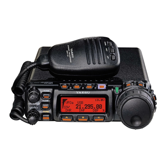
Yaesu FT-857 Technical Supplement
Hf/vhf/uhf ultra-compact transceiver
Hide thumbs
Also See for FT-857:
- Operation manual (132 pages) ,
- Technical supplement (108 pages) ,
- Manual (6 pages)
Table of Contents
Advertisement
Technical Supplement
©2003 VERTEX STANDARD CO., LTD.
Introduction
This manual provides technical information necessary for servicing the FT-857 HF/VHF/UHF Ultra-Compact Transceiver.
Servicing this equipment requires expertise in handling surface-mount chip components. Attempts by non-qualified per-
sons to service this equipment may result in permanent damage not covered by the warranty, and may be illegal in some
countries.
Two PCB layout diagrams are provided for each double-sided circuit board in the Transceiver. Each side of is referred to
by the type of the majority of components installed on that side ("leaded" or "chip-only"). In most cases one side has only
chip components, and the other has either a mixture of both chip and leaded components (trimmers, coils, electrolytic
capacitors, ICs, etc.), or leaded components only.
While we believe the technical information in this manual to be correct, VERTEX STANDARD assumes no liability for
damage that may occur as a result of typographical or other errors that may be present. Your cooperation in pointing out
any inconsistencies in the technical information would be appreciated.
Specifications .................................................. 2
Exploded View & Miscellaneous Parts ...... 5
Connection Diagram ...................................... 7
Block Diagram ................................................. 8
Circuit Description ........................................ 9
Alignment ...................................................... 12
VERTEX STANDARD CO., LTD.
4-8-8 Nakameguro, Meguro-Ku, Tokyo 153-8644, Japan
VERTEX STANDARD
US Headquarters
10900 Walker Street, Cypress, CA 90630, U.S.A.
International Division
8350 N.W. 52nd Terrace, Suite 201, Miami, FL 33166, U.S.A.
YAESU EUROPE B.V.
P.O. Box 75525, 1118 ZN Schiphol, The Netherlands
YAESU UK LTD.
Unit 12, Sun Valley Business Park, Winnall Close
Winchester, Hampshire, SO23 0LB, U.K.
VERTEX STANDARD HK LTD.
Unit 5, 20/F., Seaview Centre, 139-141 Hoi Bun Road,
EH007M90A
Kwun Tong, Kowloon, Hong Kong
Contents
Board Unit
MAIN Unit ................................................................ 23
PLL Unit ..................................................................... 49
PA Unit ...................................................................... 55
PANEL Unit .............................................................. 67
REF Unit ..................................................................... 73
PHONE-JACK Unit .................................................. 74
VR Unit ...................................................................... 75
CONNECTOR Unit .................................................. 76
DSP-2 Unit (Option) ................................................. 77
TCXO-9 Unit (Option) .............................................. 80
(Schematics, Layouts & Parts)
1
Advertisement
Table of Contents

Related Manuals for Yaesu FT-857


Summary of Contents for Yaesu FT-857
-
Page 1: Table Of Contents
Kwun Tong, Kowloon, Hong Kong Introduction This manual provides technical information necessary for servicing the FT-857 HF/VHF/UHF Ultra-Compact Transceiver. Servicing this equipment requires expertise in handling surface-mount chip components. Attempts by non-qualified per- sons to service this equipment may result in permanent damage not covered by the warranty, and may be illegal in some countries. -
Page 2: Specifications
Specifications General Frequency Range: Receive: 0.1-56 MHz, 76-108 MHz, 118-164 MHz, 420-470 MHz Transmit: 160 - 6 Meters, 2 Meters, 70 Centimeters (Amateur bands only) Emission Modes: A1 (CW), A3 (AM), A3J (LSB/USB), F3 (FM), F1 (9600 bps packet), F2 (1200 bps packet) Synthesizer Steps (Min.): 10 Hz (CW/SSB), 100 Hz (AM/FM/WFM) Antenna Impedance:... - Page 3 Specifications Receiver Circuit Type: Double-Conversion Superheterodyne (SSB/CW/AM/FM) Superheterodyne (WFM) Intermediate Frequencies: 1st: 68.33 MHz (SSB/CW/AM/FM); 10.7 MHz (WFM) 2nd: 455 kHz Sensitivity: SSB/CW 100 kHz-1.8 MHz – 32 µV – 1.8 MHz-28 MHz 0.2 µV 2 µV – 28 MHz-30 MHz 0.2 µV 2 µV 0.5 µV...
- Page 4 Note...
-
Page 5: Exploded View & Miscellaneous Parts
Exploded View & Miscellaneous Parts Non-designated parts are available only as part of a designated assembly. Ref. VXSTD P/N Description RA0471400 U00315007 PAN HEAD SCREW M3X15B SPONGE (B) U02208002 PAN HEAD SCREW SM2.6X8NI U02306002 SEMS SCREW SM3X6NI RA0459600 U20304007 BINDING HEAD SCREW M3X4B TOP CASE U24104001 TAPTITE SCREW M2X4... - Page 6 Note...
-
Page 7: Connection Diagram
Connection Diagram... -
Page 8: Block Diagram
Block Diagram... -
Page 9: Circuit Description
Circuit Description Receive Signal Circuitry filter which is matched to the receiving mode: either CF1004, CF1005 or an optional mechanical filter. RF Stages Signals between 0.1 and 56 MHz received at the antenna Noise Blanker Circuit terminal pass through a low-pass filter, selected accord- A portion of the 2nd IF signal is amplified by Noise ing to the receiving frequency, then pass to another low- Blanker Amplifiers Q 1 0 7 5 a n d Q 1 0 7 9 ( b o t h... - Page 10 Circuit Description Transmit Signal Circuitry 1st IF Circuit/1st Mixer Circuit The modulated SSB/AM signal is applied to the 2nd Mixer Microphone Amplifier Circuit Q1082 (SA602AD), which produces the 68.33 MHz 2nd The audio signal from microphone jack is amplified by IF signal utilizing the 2nd local signal (68.875 MHz).
- Page 11 Circuit Description PLL Frequency Synthesizer 2nd Local Oscillator Circuit The 2nd LO circuit is a Hartley-type overtone oscillator The PLL Frequency Synthesizer consists mainly of the circuit (frequency: 67.875 MHz) composed of Q1052 master reference oscillator circuit, 2nd local oscillator cir- (2SC4400-3) on the MAIN Unit.
-
Page 12: Alignment
Alignment Introduction and Precautions Required Test Equipment m Digital DC Voltmeter (high-Z, 1 M-Ohm/V) The following procedures cover adjustments that are not m DC Ammeter normally required once the transceiver has left the facto- m RF Millivoltmeter ry. However, if damage occurs and some parts subsequent- m AC Voltmeter ly be replaced, realignment may be required. - Page 13 Alignment Local Oscillator Adjustment PLL Adjustment Reference Frequency Adjustment VCO VCV Adjustment 1. Connect an RF millivoltmeter or an oscilloscope to 1. Connect the DC voltmeter to TP1028 on the MAIN pin 2 of J5002 on the REF Unit. Unit (or pin 6 of J2002 on the PLL Unit), and refer- 2.
- Page 14 Alignment PLL Unlock Exciter Stage Idling Current 1. Connect the DC voltmeter to TP1029 on the MAIN 1. Disconnect the Jumper Plug from J1004 on the MAIN Unit (or pin 11 of J2002 on the PLL Unit). Unit, then connect the ammeter to J1004 (pin 1: –, 2.
- Page 15 Alignment FM TX IF Adjustment TX BPF Adjustment 1. Tune the frequency to the 28 MHz band. Connect the VHF TX BPF Adjustment RF millivoltmeter to TP1033 on the MAIN Unit. 1. Set the frequency to 145.995 MHz. Disconnect the 2.
- Page 16 Alignment RX Adjustment UHF Band Alignment 1. Connect the signal generator to the 144/430 MHz an- SSB IF Adjustment tenna jack, and the DC voltmeter to TP1044 on the 1. Connect the signal generator to the HF/50 MHz an- MAIN Unit. tenna jack, and the AF milivoltmeter and the SINAD 2.
- Page 17 Alignment Power Amplifier Adjustment Directional Coupler Balance Adjustment 1. Connect the 50-Ohm dummy load to the HF/50 MHz HF/50 MHz Idling Current Adjustment antenna jack. 1. Connect the 50-Ohm dummy load to the HF/50 MHz 2. Tune the transceiver to 28 MHz band in the CW mode, antenna jack.
- Page 18 Alignment LCD Contrast Alignment Software Menu Alignment 1. Connect a DC voltmeter (High Impedance) to TP4027 The antenna jacks should be connected to a dummy load on the PANEL Unit. (in cases where transmission is involved) or the signal 2. Adjust VR4001 for an indication of –2.54 V (±0.02 generator (in the case of reception).
- Page 19 Alignment RX Gain Adjustment FM Center Meter Adjustment 1. Tune the transceiver to the 1.8 MHz band in the CW 1. Tune the transceiver to the 144 MHz band in the FM mode. mode. 2. Select “HF1RXG” in the menu by rotating the SELECT 2.
- Page 20 Alignment Over-current Protection Adjustment RF Power Adjustment 1. Set the transceiver to the CW mode. 1. Tune the transceiver to the 1.8 MHz band in the CW 2. Select menu item “18: HF1-IC.” Tune the transceiver mode. 2. Select menu item “24: HF1-MAX.” Key the transmit- to the 1.8 MHz band and key the transceiver.
- Page 21 Alignment In case the transmission power is not within the speci- ALC (Automatic Level Control) Meter Adjustment fied tolerance, adjust this parameter for 20 W (±2 W) 1. Tune the transceiver to the 21 MHz band in the USB of transmission power. mode.
- Page 22 Alignment FM Modulation Adjustment SSB Carrier Point Adjustment 1. Tune the transceiver to the 144 MHz band in the FM 1. Tune the transceiver to the 21 MHz band in the LSB mode. Connect the FM linear detector to the 144/430 mode.
-
Page 23: Main Unit
MAIN Unit Circuit Diagram... - Page 24 MAIN Unit Note:...
- Page 25 MAIN Unit Parts Layout BU4066BCFV-E2 M62352GP BU4011BF (Q1121, 1122) (Q1016) (Q1113) BU4094BCFV-E2 (Q1003, 1004, 1010) HD64F2134FA20 NJM2902V (Q1049) (Q1114, 1120) 24LC128T SA602AD KIA7808API TDA2003H 2SK2975 (Q1065) (Q1071, 1082) (Q1014) (Q1105) (Q1001, 1002) TC4W53FU (Q1038) 2SK2973 (K1) 2SA1602A (MF) 2SC4154E (LE) 2SD2211 (DQR) DTC114EU (24) (Q1006, 1007)
- Page 26 MAIN Unit Parts Layout CXA1611N AD9835BRU NJM2902V NJM2904V (Q1058) (Q1062) (Q1111, 1118, 1119) (Q1112, 1117, 1123) BU4053BCFV-E2 TC4W53FU M62364FP (Q1066) (Q1067, 1098) (Q1087) M51132FP (Q1103) TA31136FN (Q1080) 2SJ355 (PQ) 2SK2596 (BX) 2SK2685 (WV-) 2SK302Y (TY) (Q1031) (Q1011) (Q1026) (Q1083, 1084) 2SA1602A (MF) 2SC3357 (RK) 2SC4154E (LE)
-
Page 27: Parts List
MAIN Unit Parts List DESCRIPTION VALUE TOL. MFR'S DESIG VXSTD P/N VERS. LOT SIDE LAY ADR PCB with Components CP7534004 VER. A2 CP7534005 VER. A1 CP7534006 VER. A2 CP7534007 VER. A3 CP7534008 VER. B1 CP7534009 VER. B2 CP7534010 VER. B3 CP7534011 VER. - Page 28 MAIN Unit Parts List DESCRIPTION VALUE TOL. MFR'S DESIG VXSTD P/N VERS. LOT SIDE LAY ADR C 1065 CHIP CAP. 10pF GRM39CH100D50PT K22174211 C 1066 AL.ELECTRO.CAP. 100uF RC2-16V101MS(6X7) K40129038 C 1067 CHIP CAP. 0.01uF GRM39B103M50PT K22174823 C 1068 AL.ELECTRO.CAP. 10uF RV2-16V100MB55-R K48120014 C 1069...
- Page 29 MAIN Unit Parts List DESCRIPTION VALUE TOL. MFR'S DESIG VXSTD P/N VERS. LOT SIDE LAY ADR C 1144 CHIP CAP. 0.1uF GRM39B104K16PT K22124805 C 1145 CHIP CAP. 100pF UMK105CH101JW-F K22178282 C 1146 CHIP CAP. 0.01uF GRM36B103K16PT K22128804 C 1147 CHIP CAP. 0.001uF UMK105B102KW-F K22178829...
- Page 30 MAIN Unit Parts List DESCRIPTION VALUE TOL. MFR'S DESIG VXSTD P/N VERS. LOT SIDE LAY ADR C 1219 CHIP CAP. 22pF UMK105CH220JW-F K22178266 C 1221 CHIP CAP. 0.022uF EMK105B223KW-F K22128813 C 1222 CHIP CAP. 0.001uF UMK105B102KW-F K22178829 C 1223 CHIP CAP. 0.0033uF UMK105B332KW-F K22178835...
- Page 31 MAIN Unit Parts List DESCRIPTION VALUE TOL. MFR'S DESIG VXSTD P/N VERS. LOT SIDE LAY ADR C 1298 CHIP CAP. 15pF UMK105CH150JW-F K22178262 C 1299 CHIP CAP. 0.001uF UMK105B102KW-F K22178829 C 1300 CHIP CAP. 0.01uF GRM36B103K16PT K22128804 C 1301 CHIP CAP. 0.01uF GRM36B103K16PT K22128804...
- Page 32 MAIN Unit Parts List DESCRIPTION VALUE TOL. MFR'S DESIG VXSTD P/N VERS. LOT SIDE LAY ADR C 1383 CHIP CAP. 0.0015uF UMK105B152KW-F K22178831 C 1386 CHIP CAP. 220pF TMK105CH221JW-F K22148246 C 1387 CHIP TA.CAP. 10uF TEMSVA1A106M-8R K78100028 C 1388 CHIP CAP. 0.01uF GRM36B103K16PT K22128804...
- Page 33 MAIN Unit Parts List DESCRIPTION VALUE TOL. MFR'S DESIG VXSTD P/N VERS. LOT SIDE LAY ADR C 1475 CHIP CAP. 0.1uF GRM39B104K16PT K22124805 C 1476 CHIP TA.CAP. 2.2uF TESVA1A225M1-8R K78100021 C 1477 CHIP CAP. 0.1uF GRM39B104K16PT K22124805 C 1478 CHIP CAP. 0.001uF UMK105B102KW-F K22178829...
- Page 34 MAIN Unit Parts List DESCRIPTION VALUE TOL. MFR'S DESIG VXSTD P/N VERS. LOT SIDE LAY ADR C 1569 CHIP CAP. 0.1uF GRM39B104K16PT K22124805 C 1570 CHIP CAP. 0.001uF UMK105B102KW-F K22178829 C 1571 CHIP CAP. 470pF UMK105B471KW-F K22178825 C 1572 CHIP CAP. 0.001uF UMK105B102KW-F K22178829...
- Page 35 MAIN Unit Parts List DESCRIPTION VALUE TOL. MFR'S DESIG VXSTD P/N VERS. LOT SIDE LAY ADR CF1001 CERAMIC FILTER SFECV10M7FA00-R0-TC H3900537 CF1002 CERAMIC FILTER ALFYM455E=K H3900543 CF1003 CERAMIC FILTER ALFYM455G=K H3900545 CF1004 CERAMIC FILTER CFJ455K14 H3900386 CF1005 CERAMIC FILTER ALFYM455H=K H3900542 CV1001 HELICAL RESONATOR 440MHz H5T-440 440M...
- Page 36 MAIN Unit Parts List DESCRIPTION VALUE TOL. MFR'S DESIG VXSTD P/N VERS. LOT SIDE LAY ADR D 1072 DIODE DAP222-TL G2070432 D 1076 DIODE DAP222-TL G2070432 D 1077 DIODE HZM27WA-TR G2070530 D 1078 DIODE DAP222-TL G2070432 D 1079 DIODE DAP222-TL G2070432 D 1080 DIODE...
- Page 37 MAIN Unit Parts List DESCRIPTION VALUE TOL. MFR'S DESIG VXSTD P/N VERS. LOT SIDE LAY ADR JP1003 CHIP RES. 1/16W RMC1/16 000JATP J24185000 VER. C1 JP1003 CHIP RES. 1/16W RMC1/16 000JATP J24185000 VER. D1 JP1003 CHIP RES. 1/16W RMC1/16 000JATP J24185000 VER.
- Page 38 MAIN Unit Parts List DESCRIPTION VALUE TOL. MFR'S DESIG VXSTD P/N VERS. LOT SIDE LAY ADR L 1047 M.RFC 0.15uH HK1608 R15J-T L1690938 L 1048 COIL E2 0.25-1.85-8.5T-L L0022576 L 1049 COIL 05RF 2.7UH 020812327 L0022833 L 1050 M.RFC 10uH LK1608 100K-T L1690689 L 1051...
- Page 39 MAIN Unit Parts List DESCRIPTION VALUE TOL. MFR'S DESIG VXSTD P/N VERS. LOT SIDE LAY ADR Q 1054 TRANSISTOR 2SC4154-T11-1E G3341548E Q 1055 TRANSISTOR 2SC4154-T11-1E G3341548E Q 1056 TRANSISTOR 2SC4400-3-TL G3344008C Q 1057 TRANSISTOR 2SC4154-T11-1E G3341548E Q 1058 CXA1611N-T4 G1092695 Q 1059 TRANSISTOR 2SC4400-3-TL...
- Page 40 MAIN Unit Parts List DESCRIPTION VALUE TOL. MFR'S DESIG VXSTD P/N VERS. LOT SIDE LAY ADR R 1005 CHIP RES. 1/16W RMC1/16S 471JTH J24189021 R 1006 CHIP RES. 1/16W RMC1/16S 471JTH J24189021 R 1007 CHIP RES. 1/16W RMC1/16S 471JTH J24189021 R 1008 CHIP RES.
- Page 41 MAIN Unit Parts List DESCRIPTION VALUE TOL. MFR'S DESIG VXSTD P/N VERS. LOT SIDE LAY ADR R 1084 CHIP RES. 1/16W RMC1/16S 473JTH J24189045 R 1085 CHIP RES. 1/16W RMC1/16S 471JTH J24189021 R 1086 CHIP RES. 1/16W RMC1/16S 102JTH J24189025 R 1087 CHIP RES.
- Page 42 MAIN Unit Parts List DESCRIPTION VALUE TOL. MFR'S DESIG VXSTD P/N VERS. LOT SIDE LAY ADR R 1160 CHIP RES. 100k 1/16W RMC1/16S 104JTH J24189049 R 1161 CHIP RES. 1/16W RMC1/16S 101JTH J24189013 R 1162 CHIP RES. 4.7k 1/16W RMC1/16S 472JTH J24189033 R 1163 CHIP RES.
- Page 43 MAIN Unit Parts List DESCRIPTION VALUE TOL. MFR'S DESIG VXSTD P/N VERS. LOT SIDE LAY ADR R 1236 CHIP RES. 1/16W RMC1/16S 223JTH J24189041 R 1237 CHIP RES. 1/16W RMC1/16S 473JTH J24189045 R 1238 CHIP RES. 1/16W RMC1/16S 103JTH J24189037 R 1239 CHIP RES.
- Page 44 MAIN Unit Parts List DESCRIPTION VALUE TOL. MFR'S DESIG VXSTD P/N VERS. LOT SIDE LAY ADR R 1314 CHIP RES. 220k 1/16W RMC1/16S 224JTH J24189053 R 1315 CHIP RES. 1/16W RMC1/16S 101JTH J24189013 R 1316 CHIP RES. 470k 1/16W RMC1/16S 474JTH J24189057 R 1317 CHIP RES.
- Page 45 MAIN Unit Parts List DESCRIPTION VALUE TOL. MFR'S DESIG VXSTD P/N VERS. LOT SIDE LAY ADR R 1400 CHIP RES. 1/16W RMC1/16S 333JTH J24189043 R 1401 CHIP RES. 470k 1/16W RMC1/16S 474JTH J24189057 R 1402 CHIP RES. 1/16W RMC1/16S 101JTH J24189013 R 1403 CHIP RES.
- Page 46 MAIN Unit Parts List DESCRIPTION VALUE TOL. MFR'S DESIG VXSTD P/N VERS. LOT SIDE LAY ADR R 1494 CHIP RES. 1/16W RMC1/16S 103JTH J24189037 R 1495 CHIP RES. 2.2k 1/16W RMC1/16S 222JTH J24189029 R 1496 CHIP RES. 1/16W RMC1/16S 471JTH J24189021 R 1498 CHIP RES.
- Page 47 MAIN Unit Parts List DESCRIPTION VALUE TOL. MFR'S DESIG VXSTD P/N VERS. LOT SIDE LAY ADR R 1578 CHIP RES. 1.5k 1/16W RMC1/16S 152JTH J24189027 R 1579 CHIP RES. 1/16W RMC1/16S 473JTH J24189045 R 1580 CHIP RES. 1.5k 1/16W RMC1/16S 152JTH J24189027 R 1581 CHIP RES.
- Page 48 MAIN Unit Parts List DESCRIPTION VALUE TOL. MFR'S DESIG VXSTD P/N VERS. LOT SIDE LAY ADR T 1023 COIL 05RF 74.62M 010812303 L0022782 T 1024 COIL 05RF 74.62M 010812303 L0022782 T 1025 COIL 05RF 455K 010812299 L0022778 T 1026 COIL 05RF 74.62M 010812303 L0022782 T 1027...
-
Page 49: Pll Unit
PLL Unit Circuit Diagram... - Page 50 PLL Unit Parts Layout Side B Side A 2SK210GR (YG) 2SC4154E (LE) DTC124EU (25) AD9850BRS 2SC4400 (RT4) (Q2004, 2005, (Q2007) (Q2001, 2002, (Q2016) (Q2020) 2006) 2003, 2012, 2SC5374 (NA) 2013) (Q2009, 2010, 2011) UPC2713 (C1J) DAP236U (X) FQ7925 uPC1688G (C1C) (Q2022) (D2010, 2013) (Q2021)
- Page 51 PLL Unit Parts List DESCRIPTION VALUE TOL. MFR'S DESIG VXSTD P/N VERS. LOT SIDE LAY ADR PCB with Components CB1229001 Printed Circuit Board AH007M000 FR0078400 C 2001 CHIP CAP. 0.001uF UMK105B102KW-F K22178829 C 2002 CHIP CAP. 0.001uF UMK105B102KW-F K22178829 C 2003 CHIP CAP.
- Page 52 PLL Unit Parts List DESCRIPTION VALUE TOL. MFR'S DESIG VXSTD P/N VERS. LOT SIDE LAY ADR C 2080 CHIP CAP. 0.01uF GRM36B103K16PT K22128804 C 2081 CHIP CAP. 390pF UMK105B391KW-F K22178824 C 2082 CHIP TA.CAP. 10uF TEMSVA1A106M-8R K78100028 C 2084 CHIP CAP. 0.001uF UMK105B102KW-F K22178829...
- Page 53 PLL Unit Parts List DESCRIPTION VALUE TOL. MFR'S DESIG VXSTD P/N VERS. LOT SIDE LAY ADR L 2014 M.RFC 2.2uH LK1608 2R2K-T L1690634 L 2014 M.RFC 1.2uH LK1608 1R2K-T L1690845 L 2015 M.RFC 2.2uH LK1608 2R2K-T L1690634 L 2015 M.RFC 1.8uH LK1608 1R8K-T L1690847...
- Page 54 PLL Unit Parts List DESCRIPTION VALUE TOL. MFR'S DESIG VXSTD P/N VERS. LOT SIDE LAY ADR R 2053 CHIP RES. 2.2k 1/16W RMC1/16S 222JTH J24189029 R 2054 CHIP RES. 6.8k 1/16W RMC1/16S 682JTH J24189035 R 2055 CHIP RES. 220k 1/16W RMC1/16S 224JTH J24189053 R 2056...
-
Page 55: Pa Unit
PA Unit Circuit Diagram... - Page 56 PA Unit Note:...
- Page 57 PA Unit Parts Layout 2SC3102 KIA7805API 2SB1143S (Q3024) (Q3007) (Q3006) 2SC5125 (Q3023, 3023) BU4094BCFV-E2 2SD1801S (Q3003, 3012) (Q3014, 3015) 2SB624 (BV4) 2SC5374 (NA) DTA113ZK (E11) (Q3028, 3029) (Q3034) (Q3018, 3027) DTA114TK (24) DTC124GUA (K25) DTC143ZUA (123) (Q3011) (Q3010) (Q3017, 3025, 3026, 3030, 3031, 3032) DTC323TK (H02)
- Page 58 PA Unit Parts Layout 2SA812 (M5) 2SC4154E (LE) DTA113ZK (E11) (Q3013) (Q3004, 3008, (Q3019) 3009) DTC143ZUA (123) IMH6 (H6) TA75S01F (SA) (Q3016, 3033) (Q3035) (Q3001) DAN202K (N) DAP236U (X) (D3042, 3043) (D3017) DAN235U (M) (D3053) Side B...
- Page 59 PA Unit Parts List DESCRIPTION VALUE TOL. MFR'S DESIG VXSTD P/N VERS. LOT SIDE LAY ADR PCB with Components CS1785002 VER. USA CS1785003 VER. EXP (CE OFF) CS1785004 VER. AUS (CE OFF) CS1785005 VER. FRA (CE OFF) CS1785006 VER. EXP (CE ON) CS1785004 VER.
- Page 60 PA Unit Parts List DESCRIPTION VALUE TOL. MFR'S DESIG VXSTD P/N VERS. LOT SIDE LAY ADR C 3090 CHIP CAP. 0.1uF GRM42-6B104K50PT K22171820 C 3091 FILM CAP. 330pF 500V UC342H3300J-T K33279014 C 3093 CHIP CAP. 0.001uF GRM39B102K50PT K22174821 C 3095 CHIP CAP.
- Page 61 PA Unit Parts List DESCRIPTION VALUE TOL. MFR'S DESIG VXSTD P/N VERS. LOT SIDE LAY ADR C 3193 CHIP CAP. 220pF GRM39CH221J50PT K22174243 C 3194 CHIP CAP. 0.01uF GRM39B103M50PT K22174823 C 3195 CHIP CAP. 0.01uF GRM39B103M50PT K22174823 C 3197 CHIP CAP. 120pF GRM39CH121J50PT K22174237...
- Page 62 PA Unit Parts List DESCRIPTION VALUE TOL. MFR'S DESIG VXSTD P/N VERS. LOT SIDE LAY ADR C 3279 CHIP CAP. 82pF 200V GRM40CH820J200PT K22230227 C 3280 CHIP CAP. 12pF 200V GRM40CH120J200PT K22230217 C 3281 CHIP CAP. 100pF 200V GRM40CH101J200PT K22230228 C 3282 CHIP CAP.
- Page 63 PA Unit Parts List DESCRIPTION VALUE TOL. MFR'S DESIG VXSTD P/N VERS. LOT SIDE LAY ADR D 3023 DIODE HSU277TRF G2070118 D 3024 DIODE BAS316 G2070716 D 3025 DIODE BAS316 G2070716 D 3026 DIODE BAS316 G2070716 D 3027 DIODE BAS316 G2070716 D 3028 DIODE...
- Page 64 PA Unit Parts List DESCRIPTION VALUE TOL. MFR'S DESIG VXSTD P/N VERS. LOT SIDE LAY ADR L 3029 COIL 0.015uH AS0803-15NK L0022536 L 3030 CHIP COIL 4.7uH C2520C-4R7K L1690735 L 3031 COIL E2 0.4-3.0-9.5T-L L0022575 L 3032 COIL 0.047uH AS0805-47NK L0022539 L 3034 COIL...
- Page 65 PA Unit Parts List DESCRIPTION VALUE TOL. MFR'S DESIG VXSTD P/N VERS. LOT SIDE LAY ADR Q 3029 TRANSISTOR 2SB624-T2B BV4 G3206247D Q 3030 TRANSISTOR DTC143ZUA T106 G3070188 Q 3031 TRANSISTOR DTC143ZUA T106 G3070188 Q 3032 TRANSISTOR DTC143ZUA T106 G3070188 Q 3033 TRANSISTOR DTC143ZUA T106...
- Page 66 PA Unit Parts List DESCRIPTION VALUE TOL. MFR'S DESIG VXSTD P/N VERS. LOT SIDE LAY ADR R 3082 CHIP RES. 1/16W RMC1/16 471JATP J24185471 R 3083 CHIP RES. 6.8k 1/16W RMC1/16 682JATP J24185682 R 3084 CHIP RES. 1/16W RMC1/16 333JATP J24185333 R 3085 CHIP RES.
-
Page 67: Panel Unit
PANEL Unit Circuit Diagram... - Page 68 PANEL Unit Parts Layout BRPG1211C (D4008) Side A Side B HD6473032F 2SB624 (BV3) 2SC4154E (LE) PST3445UR (DF) RT1N241M (N2) S-812C50AUA HZM27WA (27A) (Q4003) (Q4007, 4009, (Q4006, 4008, (Q4004) (Q4005) (Q4002) (D4001) 4011) 4010, 4012)
- Page 69 PANEL Unit Parts List DESCRIPTION VALUE TOL. MFR'S DESIG VXSTD P/N VERS. LOT SIDE LAY ADR PCB with Compornents CB1231001 Printed Circuit Board AH007M000 FR0098400 C 4001 CHIP CAP. 470pF GRM36B471K50PT K22178805 C 4002 CHIP CAP. 470pF GRM36B471K50PT K22178805 C 4003 CHIP CAP.
- Page 70 PANEL Unit Parts List DESCRIPTION VALUE TOL. MFR'S DESIG VXSTD P/N VERS. LOT SIDE LAY ADR D 4025 19-215UYOC/S530-A2/TR8 G2070884 D 4026 19-215UYOC/S530-A2/TR8 G2070884 D 4026 19-215UYOC/S530-A2/TR8 G2070884 DS4001 LCD MODULE NCM1704A Q7000428 J 4001 CONNECTOR HJC0271-011023 P1091159 J 4002 WIRE ASSY AH007M T9207024...
- Page 71 PANEL Unit Parts List DESCRIPTION VALUE TOL. MFR'S DESIG VXSTD P/N VERS. LOT SIDE LAY ADR R 4052 CHIP RES. 1/16W RMC1/16S 393JTH J24189044 R 4053 CHIP RES. 1/16W RMC1/16S 823JTH J24189048 R 4054 CHIP RES. 3.3k 1/10W RMC1/10T 332J J24205332 R 4055 CHIP RES.
- Page 72 PANEL Unit Parts List Note DESCRIPTION VALUE TOL. MFR'S DESIG VXSTD P/N VERS. LOT SIDE LAY ADR...
-
Page 73: Ref Unit
REF Unit Circuit Diagram Parts Layout 2SC4400 (RT) (Q5001, 5002) Side A Side B Parts List DESCRIPTION VALUE TOL. MFR'S DESIG VXSTD P/N VERS. LOT SIDE LAY ADR PCB with Components CB1232001 Printed Circuit Board FR0054100 C 5001 CHIP CAP. 27pF GRM39CH270J50PT K22174221... -
Page 74: Phone-Jack Unit
PHONE-JACK Unit Circuit Diagram Parts Layout Side B Side A Parts List DESCRIPTION VALUE TOL. MFR'S DESIG VXSTD P/N VERS. LOT SIDE LAY ADR PCB with Components CB2331001 Printed Circuit Board AH007M000 FR0096600 FB4901 FERRITE BEADS BK1608HS121-T L9190081 FB4902 FERRITE BEADS BK1608HS121-T L9190081 FB4903... -
Page 75: Vr Unit
VR Unit Circuit Diagram Parts Layout Side A Side B Parts List DESCRIPTION VALUE TOL. MFR'S DESIG VXSTD P/N VERS. LOT SIDE LAY ADR PCB with Components CB2339001 Printed Circuit Board AH007M000 FR0098000 VR4801 POT. RK0972210 10KB/10KB J62800141... -
Page 76: Connector Unit
CONNECTOR Unit Circuit Diagram Parts Layout Side A Side B Parts List DESCRIPTION VALUE TOL. MFR'S DESIG VXSTD P/N VERS. LOT SIDE LAY ADR PCB with Components CB2338001 Printed Circuit Board AH007M000 FR009820B J 7001 CONNECTOR HJC0278-010022 P1091164 J 7002 WIRE ASSY AH007M T9207023... -
Page 77: Dsp-2 Unit (Option)
DSP-2 Unit (Option) Circuit Diagram Parts Layout AK7712VT (Q6003) Side A NJM2902V (Q6001, 6002) DTC114EU (24) (Q1053) Side B... - Page 78 DSP-2 Unit (Option) Parts List DESCRIPTION VALUE TOL. MFR'S DESIG VXSTD P/N VERS. LOT SIDE LAY ADR Printed Circuit Board AAC62X000 FR0079600 C 6001 CHIP CAP. GRM40B105K10PT K22100802 C 6002 CHIP CAP. GRM40B105K10PT K22100802 C 6004 CHIP CAP. 0.01uF GRM36B103K16PT K22128804 C 6005 CHIP CAP.
- Page 79 DSP-2 Unit (Option) Parts List DESCRIPTION VALUE TOL. MFR'S DESIG VXSTD P/N VERS. LOT SIDE LAY ADR R 6032 CHIP RES. 1/16W RMC1/16S 471JTH J24189021 R 6033 CHIP RES. 1/16W RMC1/16S 471JTH J24189021 R 6034 CHIP RES. 1/16W RMC1/16S 471JTH J24189021 R 6035 CHIP RES.
-
Page 80: Tcxo-9 Unit (Option)
TCXO-9 Unit (Option) Circuit Diagram Parts Layout Side A Side B Parts List DESCRIPTION VALUE TOL. MFR'S DESIG VXSTD P/N VERS. LOT SIDE LAY ADR Printed Circuit Board FR005860C C 5101 CHIP CAP. 0.01uF GRM39B103K25PT K22144803 C 5102 CHIP TA.CAP. 10uF 6.3V TESVSP0J106M-8R... - Page 82 Copyright 2003 VERTEX STANDARD CO., LTD. All rights reserved No portion of this manual may be reproduced without the permission of VERTEX STANDARD CO., LTD. Printed in Japan.