Table of Contents
Advertisement
Quick Links
Download this manual
See also:
Instruction Manual
SERVICE MANUAL
SERVICE MANUAL
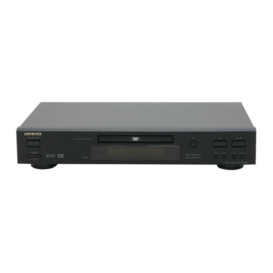
DVD PLAYER
DV-SP302
MODEL
Black, Silver and Golden models
CDD
120V AC, 60Hz
CUA, CUT,
100-240V AC, 50/60Hz
CUK, CUR
SAFETY-RELATED COMPONENT
WARNING!!
THE MARK
FOUND ON SOME COMPONENT
PARTS INDICATES THE CRITICAL FOR RISK OF
FIRE AND ELECTRIC SHOCK.
WHEN REPLACING, BE SURE TO USE PARTS OF
IDENTICAL DESIGNATION.
MAKE LEAKAGE-CURRENT OR RESISTANCE
MEASUREMENTS TO DETERMINE THAT EXPOSED
PARTS ARE ACCEPTABLY INSULATED FROM THE
SUPPLY CIRCUIT BEFORE RETURNING THE
APPLIANCE TO THE CUSTOMER.
DV-SP302
Ref. No. 3814
092004
RC-575DV
Advertisement
Table of Contents

Related Manuals for Onkyo DV-SP302


Summary of Contents for Onkyo DV-SP302
-
Page 1: Dvd Player
DV-SP302 Ref. No. 3814 092004 SERVICE MANUAL SERVICE MANUAL DVD PLAYER DV-SP302 MODEL RC-575DV Black, Silver and Golden models 120V AC, 60Hz CUA, CUT, 100-240V AC, 50/60Hz CUK, CUR SAFETY-RELATED COMPONENT WARNING!! THE MARK FOUND ON SOME COMPONENT PARTS INDICATES THE CRITICAL FOR RISK OF FIRE AND ELECTRIC SHOCK. -
Page 2: Specifications
DV-SP302 SPECIFICATIONS DVD Player Power supply AC 120 V, 60 Hz (North America models) AC 100-240 V, 50/60 Hz (Other models) Power consumption 16 W Weight 6.6 lbs, 3.0 kg External dimensions (W x H x D) 17-1/8" x 3-3/16" x 11-1/8"... -
Page 3: Service Procedure
DV-SP302 SERVICE PROCEDURE-1 SAFETY CHECK (Only U.S.A. model) After correcting the original service problem perform the AVIS following safety check before releasing the set to the customer WARNING RISK OF ELECTRIC SHOCK RISOUE DE CHOC ELECTRIQUE Connect the insulating-resistance tester between the plug of... - Page 4 DV-SP302 SERVICE PROCEDURE-2 Replace the DVD mechanism Bottom side 1. Remove the top cover (six screws) 2. Remove two screws of both side of front panel. 3. Remove the bracket mecha. (two screws). 4. Shift the cam slider on bottom side. (See Fig-1) 5.
-
Page 5: Exploded View
EXPLODED VIEW S3 x 2 1) Insert a plate in a panel front. Thereafter 2) Insert a wire in a hole of palte and do soler. S2 x 2 S2 x 4 S2 x 2 S7 x2... - Page 6 DV-SP302 S3 x 3 S4 x 11 S1 x 3 S2 x 2 S3 x 2 S2 x 4 S1 : 3 x 18 W/ Washer S2 : 3 x 8 ZNY/ BH S3 : 3 x 10 BK/ BH...
- Page 7 DV-SP302 EXPLODED VIEW S3 x 2 S3 x 3 1) Insert a plate in a panel front. Thereafter 2) Insert a wire in a hole of palte and do soler. S4 x 11 S2 x 2 S1 x 3 S2 x 2...
- Page 8 DV-SP302 BLOCK DIAGRAM FRONT DISPLAY SECTION...
- Page 9 BLOCK DIAGRAM OVERALL...
- Page 10 DV-SP302...
- Page 11 DV-SP302 BLOCK DIAGRAM OVERALL...
-
Page 12: Schematic Diagram
SCHEMATIC DIAGRAM : DVD MAIN CIRCUIT BOARD-2/2... - Page 13 DV-SP302 From Power supply unit...
- Page 14 : DVD MAIN CIRCUIT PC BOARD-2/2 SCHEMATIC DIAGRAM...
- Page 15 DV-SP302 PB (UDAC) PR (CDAC) Y (YDAC) COMP. Y (YDAC) SVIDEO CVBS (VDAC) C (FDAC) V-MUTE...
- Page 16 SCHEMATIC DIAGRAM : FRONT DISPLAY PC BOARD U4-1 : FL TUBE PC BOARD From FL tube bo U4-4...
- Page 17 DV-SP302 : OUTPUT TERMINAL PC BOARD U4-2 : KEY SWITCH PC BOARD be board To DVD main board : REMOTE SENSOR PC BOARD To FL display board Optical Coaxial U4-3 : STANDBY SWITCH PC BOARD...
- Page 18 DV-SP302 SCHEMATIC DIAGRAM : FRONT DISPLAY PC BOARD : OUTPUT TERMINAL PC BOARD U4-2 : KEY SWITCH PC BOARD U4-1 : FL TUBE PC BOARD From FL tube board To DVD main board U4-4 : REMOTE SENSOR PC BOARD To FL display board...
- Page 19 DV-SP302 SCHEMATIC DIAGRAM : DVD MAIN CIRCUIT BOARD-2/2 From Power supply unit...
- Page 20 DV-SP302 : DVD MAIN CIRCUIT PC BOARD-2/2 SCHEMATIC DIAGRAM PB (UDAC) PR (CDAC) Y (YDAC) COMP. Y (YDAC) SVIDEO CVBS (VDAC) C (FDAC) V-MUTE...
- Page 21 DV-SP302 PCBOARD CONNECTION DIAGRAM OUTPUT TERMINAL BOARD POWER SUPPLY UNIT MECHA. PICK-UP CMS-S71SG6C DVD MAIN BOARD U4-3 STANDBY U4-1 U4-2 SWITCH BOARD FL TUBE BOARD SWITCH BOARD U4-4 REMOTE SENSOR BOARD U4 FRONT DISPLAY BOARD: (U4-1) + (U4-2) + (U4-3) + (U4-4)
- Page 22 DV-SP302 PRINTED CIRCUIT BOARD VIEW FROM COMPONENT SIDE-3 : FRONT DISPLAY BOARD U4-1 : FL TUBE BOARD U4-2 : KEY SWITCH BOARD C943 C942 C941 C940 C939 C938 C937 C936 R904 C935 R903 C934 C933 C932 R902 C931 C930 R901...
-
Page 23: Printed Circuit Board View
DV-SP302 PRINTED CIRCUIT BOARD VIEW-1 DVD MAIN BOARD-1 Top view... - Page 24 DV-SP302 PRINTED CIRCUIT BOARD VIEW-2 DVD MAIN BOARD-2 Bottom view...
- Page 25 DV-SP302 PRINTED CIRCUIT BOARD VIEW FROM SOLDERING SIDE-4 OUTPUT TERMINAL PC BOARD Component side view CN81...
- Page 26 DV-SP302 PRINTED CIRCUIT BOARD VIEW FROM SOLDERING SIDE-5 OUTPUT TERMINAL PC BOARD Soldering side view...
- Page 27 DV-SP302 IC BLOCK DIAGRAM/ TERMINAL DESCRIPTION IC6 : BA5954 MOTOR DROVER...
- Page 28 DV-SP302 IC BLOCK DIAGRAM/ TERMINAL DESCRIPTION IC2 : ES6603 DVD SERVO F/E-(1) ES6603S...
- Page 29 DV-SP302 IC BLOCK DIAGRAM/ TERMINAL DESCRIPTION IC2 : ES6603 DVD SERVO F/E-(2) Name Pin Numbers Definition DVDRFP, 1, 2 Differential RF signal attenuator inputs. DVDRFN AC coupled photo detector interface inputs for the differential phase detector (DPD) A2, B2, C2, D2 from the main beam photo matrix.
- Page 30 DV-SP302 IC BLOCK DIAGRAM/ TERMINAL DESCRIPTION IC2 : ES6603 DVD SERVO F/E-(3) Name Pin n Numbers I/ I/O Definition enter r error r ou output t referen ence t to V V125 p pin in 3 36. 6. MNTR onitor r ou out t sig ignal al.
- Page 31 DV-SP302 IC BLOCK DIAGRAM/ TERMINAL DESCRIPTION IC2 : ES6603 DVD SERVO F/E-(4) Block diagram FCCR b6-0 CDR b6 RFCR b3 HLDEN FBCR b6-0 AGC HOLD CGR b1 PROGRAMMABLE DVDRFP OUTPUT INHIBIT EQUALIZER IMPUT FULL WAVE FILTER CHARGE DVDRFN BIAS RECTI IER...
-
Page 32: Pinout Diagram
DV-SP302 IC BLOCK DIAGRAM/ TERMINAL DESCRIPTION IC10 : ES6629 VIDEO PROCESSOR-(1) PINOUT DIAGRAM AVSS_DS VD33_PL AVSS_PL PDOFTR1 RBCK FTROPI AVDD3_PL PLLFTR1 PLLFTR2 VREF0 VD33 AWRC VS33 AVSS_DA RFRPCTR TRAY AVDD3_DA SPINDLE LOE# FOCUS LWRLL# SLEGP LCS3# SLEGN TRACK TESTDA LCS2#... -
Page 33: Pin Description
DV-SP302 IC BLOCK DIAGRAM/ TERMINAL DESCRIPTION IC10 : ES6629 VIDEO PROCESSOR-(2) PIN DESCRIPTION Table 1 ES6629 Pin Description Names Pin Numbers Definitions 1, 10, 19, 35, 44, VD33 53, 62, 79, 96, 126, I/O power supply. VID_XI Crystal input. VID_XO Crystal output. - Page 34 DV-SP302 IC BLOCK DIAGRAM/ TERMINAL DESCRIPTION IC10 : ES6629 VIDEO PROCESSOR-(3) Table 1 ES6629 Pin Description (Continued) Names Pin Numbers Definitions RSET DAC current adjustment resistor input. YUV4 YUV pixel 4 output data. FDAC Video DAC output. Refer to description and matrix for UDAC pin 115.
- Page 35 DV-SP302 IC BLOCK DIAGRAM/ TERMINAL DESCRIPTION IC10 : ES6629 VIDEO PROCESSOR-(4) Table 1 ES6629 Pin Description (Continued) Names Pin Numbers Definitions Audio transmit frame sync output. SEL_PLL2 System and DSCK output clock frequency selection is made at the rising edge of RESET#.
- Page 36 DV-SP302 IC BLOCK DIAGRAM/ TERMINAL DESCRIPTION IC10 : ES6629 VIDEO PROCESSOR-(5) Table 1 ES6629 Pin Description (Continued) Names Pin Numbers Definitions Audio transmit frame sync output. SEL_PLL2 System and DSCK output clock frequency selection is made at the rising edge of RESET#.
- Page 37 DV-SP302 IC BLOCK DIAGRAM/ TERMINAL DESCRIPTION IC10 : ES6629 VIDEO PROCESSOR-(6) Table 1 ES6629 Pin Description (Continued) Names Pin Numbers Definitions AVSS_AD Analog ground for ADC block. Center error input signal. Tracking error input signal. RFRP RF ripple/envelope input signal.
- Page 38 DV-SP302 IC BLOCK DIAGRAM/ TERMINAL DESCRIPTION IC10 : ES6629 VIDEO PROCESSOR-(7) Table 1 ES6629 Pin Description (Continued) Names Pin Numbers Definitions PHOI Sledge photo interrupt signal input. SCSJ Chip selection signal to RF chip (serial data enable). SDATA Data signal from/to RF chip.
-
Page 39: System Block Diagram
SV-SP302 IC BLOCK DIAGRAM/ TERMINAL DESCRIPTION IC10 : ES6629 VIDEO PROCESSOR-(8) SYSTEM BLOCK DIAGRAM A sampling system block diagram for the ES6629 Vibratto-II DVD player board design is shown in Figure 2. DVD/CD Motor Motor Driver Video ES6603 T V Display RF Amp 8/16-MB Audio DAC... -
Page 40: Pin Configuration
DV-SP302 IC BLOCK DIAGRAM/ TERMINAL DESCRIPTION IC9 : HY57V641620HG D RAM-(1) PIN CONFIGURATION V SS D Q 0 D Q 1 5 VDDQ V SSQ D Q 1 D Q 1 4 D Q 2 D Q 1 3 VSSQ... -
Page 41: Functional Block Diagram
DV-SP302 IC BLOCK DIAGRAM/ TERMINAL DESCRIPTION IC9 : HY57V641620HG D RAM-(2) FUNCTIONAL BLOCK DIAGRAM S e l f r e f r e s h l o g i c I n t e r n a l R o w &... - Page 42 DV-SP302 IC BLOCK DIAGRAM/ TERMINAL DESCRIPTION IC8 : M24C02WMN6 EEPROM Logic Diagram V CC E0-E2 M24Cxx V SS Signal Names E0, E1, E2 Chip Enable Inputs Serial Data/Address Input/ Output Serial Clock Write Control Supply Voltage Ground SO Connections M24Cxx...
- Page 43 DV-SP302 IC BLOCK DIAGRAM/ TERMINAL DESCRIPTION IC12 : M29W800DT MEMORY FLASH LOgic Diagram Signal Names TSOP Connections...
-
Page 44: Pin Connections
DV-SP302 IC BLOCK DIAGRAM/ TERMINAL DESCRIPTION IC81 : M74HCU04 INVERTER IC PIN CONNECTIONS PIN DESCRIPTION... - Page 45 DV-SP302 IC BLOCK DIAGRAM/ TERMINAL DESCRIPTION IC14 : MM1507 VIDEO SWITCH Block Diagram Measuring circuit...
-
Page 46: Block Diagram
DV-SP302 IC BLOCK DIAGRAM/ TERMINAL DESCRIPTION IC15 : WM8761 D/D Converter BLOCK DIAGRAM CONTROL INTERFACE WM8761 SIGMA DELTA PASS MUTE VOUTR BCKIN IN MODULATOR FILTER UDIO RCIN IN DIGI GITAL F FILTERS INTERFACE DIN IN SIGMA MUTE DELTA PASS PASS... - Page 47 DV-SP302 FL TUBE VIEW FL91 : HNV-12SM69T GRID ASSIGNMENT PROGRESSIVE PROGRESSIVE TITLE TITLE CHAPTER CHAPTER TRACK TRACK HOUR HOUR MEM. MEM. INTRO INTRO REPEAT REPEAT 1 ALLA-B 1 ALLA-B RESUME RESUME RANDOM RANDOM (2G - 11G) ANODE CONNECTION...
- Page 48 DV-SP302 IC BLOCK DIAGRAM/ TERMINAL DESCRIPTION IC91 : uPD16311 FL Driver-(1) PIN CONFIGURATION Grid Grid Grid /Grid /Grid /Grid /Grid /Grid /Grid /Grid /Grid...
- Page 49 DV-SP302 IC BLOCK DIAGRAM/ TERMINAL DESCRIPTION IC91 : uPD16311 FL Driver-(2) BLOCK DIAGRAM Dimming Command decoder circuit Display memory Serial I/F 20 bit x 16 word /Grid Timming generator key scan /Grid Key data memory (4 x 12) Grid Grid...
-
Page 50: Pin Function
DV-SP302 IC BLOCK DIAGRAM/ TERMINAL DESCRIPTION IC91 : uPD16311 FL Driver-(3) PIN FUNCTION Pin No. Symbol Pin name Description Inputs serial data at rising edge of shift clock, Data input starting from lower bit. DOUT Data output Outputs serial data at falling edge of shift clock, starting from lower bit. -
Page 51: Upgrade Firmware
4. While display version of firmware, turn off a mechanical power switch. Upgrade the firmware 1. Connect a video monitor to video out jack on the DV-SP302. 2. Turn on the power switch and standby switch on. 3. Setting the disc on the tray. (Down load firmware data disc) 4. - Page 52 STEP 1 : LABEL FOR SET POSITION DETAIL - CARD CERTIFICATE Rear side Front side Rear side Apply to DV-SP302 CUR6P only Stick in the card certificate Record trier's name and data before packing in card certificate. Changed packing location...
- Page 53 Roll a PE bag and attach tape to PE bag. (2 place) EP 5 : AC CORD POSITION Stick in the accessory Not apply to DV-SP302 CUR6P (CHINA VERSION ONLY) STEP 7 : LABEL FOR BOX POSITION For Rear panel Stick in the accessory...
- Page 54 STEP 2 : KNOB POWER POSITION POWER STEP 5 : AC CORD POSITION Knob power position : ON Stick in the accessory Not apply to DV-SP302 CUR6P (CHINA VERSION ONLY) OFF (NG) ON (OK) NOTE Pack the unit that have been set the DVD mechanism to initial mode (Push standby button so that set can goes into standby mode.
-
Page 55: Packing Parts List
55932760 POS Label <S CUA4P> AC PRI LABEL POS DV-SP302(S) CUA4P 55932740 POS Label <G CUT3P> <G CUK3P> <G CUR6P> AC PRI LABEL POS DV-SP302(G) CUT3P 55169520 Sheet AC RAW BAG SHEET EPE TAV5100 820MM X 820MM 5568332A Pad L... - Page 56 AC RAW SHIELD COVER SENSOR DV-C503 55186710 Facet AC MLD CRYSTAL ST/BY DV-C503 55830650 Front display board <B CDD1N> AC EMBD IMA FRONT BD DV-SP302(B) CDD1N 55931380 Front display board <B CUA4P> AC EMBD IMA FRONT BD DV-SP302(B) CUA4P 55931390 Front display board <S CDD1N>...
- Page 57 55932620 Rear panel <B> <CUA4P> AC CPL REAR PANEL DV-SP302(B) CUA4P REAR PANEL 55932630 Rear panel <G> <CUT3P> <CUK3P> AC CPL REAR PANEL DV-SP302(G) CUT3P 55932640 Rear panel AC CPL REAR PANEL DV-SP302(G) CUR6P <G> <CUR6P> 55125180 Bushing AC MLD CLAMP AC CORD RT2280/RT2250(PAV5007/PAV5005)
- Page 58 AC PUN COVER TOP DV-SP301(G) UUS4P PCM 0.7T GD01TH 55896680 DVD Loader mechanism AC MSA ASY WXD-8610(2) DVD LOADER 55926240 Frame AC PUN BRACKET FRAME MECHA DV-SP302 SECC 1.0T 5516498A Spacer AC MLD BRACKET SPACE PCB BK PLASTIC 55943700 Traverse mechanism AC MSA ASY PICK-UP TRAVERSE CMS-S71SG6T...
-
Page 59: Pc Board Parts List
DV-SP302(B) UDD1N PART LIST PC BOARD PARTS LIST FRONT DISPLAY BOARD DV-SP302 CIRCUIT NO. PART NAME PART NO. DESCRIPTION 0050 Holder 55832580 front FL tube CN61 Socket AS 55180520 5P 220mm, 2.0mm CN62 Socket AS 55951950 9P 130mm, 2.0mm CN63... - Page 60 DV-SP302(B) UDD1N PART LIST D903 Diode 70436540 D-SLP 1N4148 100.0V 150E-3A R601 Resistor 30939360 RCF 10R0 OHM +5% 250MI0W R602 Resistor 30939370 RCF 15R0 OHM +5% 250MI0W R603 Resistor 30939370 RCF 15R0 OHM +5% 250MI0W R604 Resistor 30939370 RCF 15R0 OHM +5% 250MI0W...
- Page 61 DV-SP302(B) UDD1N PART LIST Capacitor 20506540 CCCFMIC 10P0F +0P5F -0P5F 50.0V NP0 Capacitor 20506540 CCCFMIC 10P0F +0P5F -0P5F 50.0V NP0 Capacitor 20506540 CCCFMIC 10P0F +0P5F -0P5F 50.0V NP0 Capacitor 20506680 CCCFMIC 470P0F +5% -5% 50.0V NP0 Capacitor 20506540 CCCFMIC 10P0F +0P5F -0P5F 50.0V NP0...
- Page 62 DV-SP302(B) UDD1N PART LIST Resistor 10134710 RMGCFMIC 75R0 OHM +5% 100MI0W Resistor 10135010 RMGCFMIC 10K0 OHM +5% 100MI0W Resistor 10135010 RMGCFMIC 10K0 OHM +5% 100MI0W Resistor 10328750 RMGCFMIC 0 OHM +0% 100MI0W Resistor 10328750 RMGCFMIC 0 OHM +0% 100MI0W Resistor...
- Page 63 DV-SP302(B) UDD1N PART LIST Capacitor 20506680 CCCFMIC 470P0F +5% -5% 50.0V NP0 Capacitor 20678060 CCCFMIC 27P0F +5% -5% 50.0V NP0 Capacitor 20678060 CCCFMIC 27P0F +5% -5% 50.0V NP0 Capacitor 10138550 CCCFMIC 1N0F +10% -10% 50.0V X7R Capacitor 20288040 CCCFMIC 100N0F +80% -20% 16.0V Y5V...
- Page 64 DV-SP302(B) UDD1N PART LIST D802 Diode 20496510 D-SLP 1SS355 35.0V 225MI0A D803 Diode Zener 55171070 D-ZENER UDZS 2.2 B 2.2V 200MI0W D804 Diode 20496510 D-SLP 1SS355 35.0V 225MI0A Diode 20496510 D-SLP 1SS355 35.0V 225MI0A Diode 20496510 D-SLP 1SS355 35.0V 225MI0A...
- Page 65 DV-SP302(B) UDD1N PART LIST Resistor 10135940 RMGCFMIC 4K7 OHM +5% 100MI0W R101 Resistor 10134830 RMGCFMIC 220R0 OHM +5% 100MI0W Resistor 10328750 RMGCFMIC 0 OHM +0% 100MI0W R154 Resistor 10134830 RMGCFMIC 220R0 OHM +5% 100MI0W R157 Resistor 10328750 RMGCFMIC 0 OHM +0% 100MI0W...
- Page 66 DV-SP302(B) UDD1N PART LIST R827 Resistor 10134410 RMGCFMIC 10R0 OHM +5% 100MI0W R828 Resistor 10135220 RMGCFMIC 47K0 OHM +5% 100MI0W R829 Resistor 10134740 RMGCFMIC 100R0 OHM +5% 100MI0W R830 Resistor 10135340 RMGCFMIC 100K0 OHM +5% 100MI0W R832 Resistor 10135820 RMGCFMIC 1K5 OHM +5% 100MI0W...
- Page 67 DV-SP302(B) UDD1N PART LIST RS27 Resistor 10134590 RMGCFMIC 33R0 OHM +5% 100MI0W Resistor 10135900 RMGCFMIC 3K3 OHM +5% 100MI0W RS37 Resistor 10328750 RMGCFMIC 0 OHM +0% 100MI0W RS39 Resistor 10328750 RMGCFMIC 0 OHM +0% 100MI0W Resistor 10135900 RMGCFMIC 3K3 OHM +5% 100MI0W...
- Page 68 DV-SP302(B) UDD1N PART LIST D814 Diode 55177710 D-ZENER UDZS 5.1 B 5.1V 200MI0W D815 Diode 55177710 D-ZENER UDZS 5.1 B 5.1V 200MI0W D816 Diode 55177710 D-ZENER UDZS 5.1 B 5.1V 200MI0W D817 Diode 55177710 D-ZENER UDZS 5.1 B 5.1V 200MI0W...
- Page 69 Tel: 201-785-2600 Fax: 201-785-2650 http://www.onkyousa.com ONKYO EUROPE ELECTRONICS GmbH Liegnitzerstrasse 6, 82194 Groebenzell, GERMANY Tel: +49-8142-4401-0 Fax: +49-8142-4401-555 http://www.onkyo.net ONKYO CHINA LIMITED Units 2102-2107, Metroplaza Tower I, 223 Hing Fong Road, Kwai Chung, N.T., HONG KONG Tel: 852-2429-3118 Fax: 852-2428-9039 HOMEPAGE http://www.onkyo.com/...