Sony CDP-XA30ES Service Manual
Hide thumbs
Also See for CDP-XA30ES:
- Operating instructions manual (112 pages) ,
- Operating instructions manual (112 pages)
Table of Contents
Advertisement
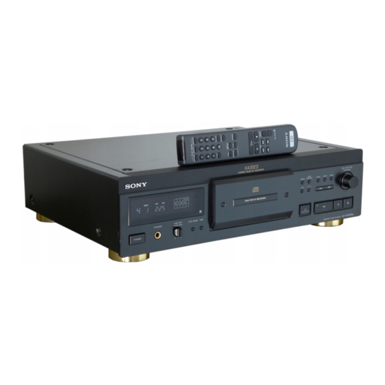
CDP-XA30ES
SERVICE MANUAL
AEP Model
E Model
Photo : Gold
Model Name Using Similar Mechanism
NEW
CD Mechanism Type
CDM36A-14A
Base Unit Type
BU-14A
Optical Pick-Up Type
KSS-213B
SPECIFICATIONS
– Continued on next page –
COMPACT DISC PLAYER
MICROFILM
Advertisement
Table of Contents

Related Manuals for Sony CDP-XA30ES


Summary of Contents for Sony CDP-XA30ES
- Page 1 CDP-XA30ES SERVICE MANUAL AEP Model E Model Photo : Gold Model Name Using Similar Mechanism CD Mechanism Type CDM36A-14A Base Unit Type BU-14A Optical Pick-up Type KSS-213B SPECIFICATIONS – Continued on next page – COMPACT DISC PLAYER MICROFILM...
-
Page 2: Table Of Contents
LINE WITH MARK ! ON THE SCHEMATIC DIAGRAMS AND IN THE PARTS LIST ARE CRITICAL TO SAFE OPERATION. REPLACE THESE COMPONENTS WITH SONY PARTS WHOSE PART NUMBERS APPEAR AS SHOWN IN THIS MANUAL OR IN SUPPLEMENTS PUB- LISHED BY SONY. -
Page 3: Servicing Notes
SECTION 1 SERVICING NOTES 1-1. HOW TO OPEN THE DISC TRAY WHEN NOTES ON HANDLING THE OPTICAL PICK-UP POWER SWITCH TURNS OFF BLOCK OR BASE UNIT 1 Insert a tapering driver into the aperture of the unit bottom, The laser diode in the optical pick-up block may suffer electro- and move the limiter (LEVER) to direction of the arrow A. -
Page 4: General
SECTION 2 This section is extracted from instruction manual. GENERAL – 4 –... - Page 5 – 5 –...
- Page 6 – 6 –...
- Page 7 – 7 –...
- Page 8 – 8 –...
- Page 9 – 9 –...
- Page 10 – 10 –...
- Page 11 – 11 –...
- Page 12 – 12 –...
- Page 13 – 13 –...
- Page 14 – 14 –...
-
Page 15: Disassembly
SECTION 3 DISASSEMBLY • This set can be disassembled in the order shown below. LOADING PANEL CASE, MECHANISM BASE UNIT OPTICAL PICK-UP FRONT PANEL SECTION DECK SECTION SECTION (Page 17) (Page 17) (Page 16) (Page 16) (Page 15) LOADING MOTOR (Page 18) POWER BOARD, MAIN BOARD (Page 18) - Page 16 CASE, FRONT PANEL SECTION 3 case 1 four screws (CASE 3 TP2) 2 screw (BVTT3 × 6) 7 connector (CN407) 1 four screws (CASE 3 TP2) 9 connector (CN992) HP board 0 two screws 8 connector (BVTT3 × 6) 4 connector (CN402) (CN206) 5 flat wire (10 core)
- Page 17 6 two screws BASE UNIT (BVTP3 × 8) 3 panel (DRAWER) 2 two screws (BVTP3 × 8) 7 panel (R) (DRAWER) 9 screw (BVTP3 × 8) 8 flat wire (30 core) !º lug (CN108) !¡ base unit (BU-14A) 5 cover (F) (DRAWER) 2 two screws (BVTP3 ×...
- Page 18 4 screw LOADING MOTOR (BVTP 3 × 8) 7 Removal the two solders of loading motor. 1 Pull the tray. 6 LOADING MOTOR board 8 loading motor 5 two claws 2 connector (CN103) 3 Hang the belt 1 two connectors 2 two connectors POWER BOARD, MAIN BOARD (CN207, 309)
-
Page 19: Af Mode
SECTION 4 TEST MODE 4-1. AF MODE Keep pressing the §OPEN/CLOSE button, and all on display is attained again. Connect the TP19 (AFADJ) on the BD board to the ground and turn on the power supply. 4-1-2. Key Check The AF mode is then activated and the following check can be made. -
Page 20: Adj Mode
4-2. ADJ MODE Connecting Location: [BD BOARD] (SIDE B) Connect the TP18 (ADJ) on the BD board to the ground and turn on the power supply. The ADJ mode is then activated and the following operation is executed. IC361 TP18 TP19 •... -
Page 21: Electrical Adjustments
SECTION 5 ELECTRICAL ADJUSTMENTS Connecting Location: Notes: RF signal waveform [BD BOARD] (SIDE B) 1. CD block basically constructed to operate without adjustment. VOLT/DIV: 200 mV Therefore, check each item in order given. TIME/DIV: 500 ns (with the 10: 1 probe 2. -
Page 22: Ic Pin Function Discription
SECTION 6 DIAGRAMS 6-1. IC PIN FUNCTION DISCRIPTION BD BOARD IC101 CXD2545Q (DIGITAL SIGNAL PROCESSOR, FOCUS/TRACKING/SLED SERVO, EFM COMPARATOR) Pin No. Pin Name I / O Function Pin No. Pin Name I / O Function SRON Sled servo drive PWM signal output terminal Not used (open) WDCK Word clock signal (88.2 kHz) output terminal... - Page 23 Pin No. Pin Name Function SBSO Sub-code P-W serial data output terminal Not used (open) EXCK Sub-code P-W serial data reading clock signal input terminal Not used (fixed at “L”) SUBQ Sub-code Q data signal output to the system controller (IC351) SQCK Sub-code Q data reading clock signal input from the system controller (IC351) MUTE...
- Page 24 • BD BOARD IC351 CXP84124-068Q (SYSTEM CONTROL) Pin No. Pin Name Function Address signal output to the static RAM (IC352) Write enable signal output to the static RAM (IC352) Not used (open) Not used (open) ( LED (D871) drive signal output terminal “H”: LED on LED-PLAY LED-PAUSE P LED (D872) drive signal output terminal “H”: LED on...
- Page 25 Pin No. Pin Name Function Key input terminal (A/D input) EDIT/TIME FADE, REPEAT, FILE, § OPEN/CLOSE, (, P, p keys (S811 to S817) input Rotary encoder input terminal (A/D input) AMS ± key (RV801) input Rotary encoder input terminal (A/D input) AMS ≠ key (RV801) input IN/OUT SW Detection input from the loading in/out detect switch (S281, S282) (A/D input) SCLK...
- Page 26 @¶) SENSER SW (pin Main Ports !¶) As IC361 IS471F operate in pulse as shown in the figure, the SPDL-MUTE (pin sound quality may be affected if operated constantly. As the From the viewpoint of performance of the set, the disc must purpose of IC361 is to detect if the presence of the stabilizer, not move nor sway when the disc table opens.
-
Page 27: Ic Block Diagrams
• IC Block Diagrams – BD Section – IC103 CXA1821M LD ON – – LC/PD APC LD AMP VREF RF EQ AMP – – RF SUMMING AMP – FOCUS ERROR AMP FE BIAS TRACKING ERROR AMP – – VC BUFFER –... -
Page 28: Main Section
– MAIN Section – IC206 M51957AL – IC301 CXD8595Q TIMING CIRCUIT IF SELD S / P INAF "0" DETECT IF SELC OVFLAG MUTE CIRCUIT MUTER SBCKI MUTEL MODE 4BIT DATA 3rd order L . I . P. NOISE SDATAR MTPOL SHAPER BITSTREAM x 0.75... - Page 29 IC302 CXD2562Q 51 50 49 48 47 TIMING CIRCUIT SYNC COEF SPLM INTERPOLATER DATAOUT 18/20 ON/OFF INTERPOLATER DVDDR TEST1 VSUB (D) R TEST2 VSUB (CHIP) R THIRD ORDER TEST3 NOISE SHAPER VDD2 DVDDL VSUB (D) L R1 (–) VSUB (CHIP) L THIRD ORDER VDD2 NOISE SHAPER...
-
Page 30: Panel Section
IC501, 601 CXA8042AS I01+ IN2– I02– IN2+ I01– IN1+ SWITCHING IN1– I02+ CIRCUIT VCC2 GND2 VEE2 VCC1 CONSTANT REFERENCE VEE1 VREF CURRENT VOLTAGE CIRCUIT CIRCUIT CONTROL CIRCUIT VCNT CIREF GND1 RIREF – PANEL Section – IC801, 802, 803 LC7570E 45 44 43 42 41 40 39 38 37 NC 1 SHIFT REGISTER A/D CONVERTER... - Page 31 • Wave forms – MAIN BOARD – 1 IC302 !º (XIN) 6 IC101 $∞ (LRCK) 2.02 Vp-p 6.32 Vp-p 45.455 MHz 44.053 kHz – BD BOARD – 7 IC101 #§ (RFAC) 2 IC351 #™ (XOUT) 200 mV/DIV, 500 nS/DIV +0.25 1.25 Vp-p –0.20...
- Page 32 • Circuit Boards Location VOL SEL board BD board POWER board HP board LOADING MOTOR board DISPLAY board LOADING SW board POWER SW board MAIN board BSL board BD TRANSLATION board PANEL board – 34 –...
-
Page 40: Exploded Views
SECTION 7 EXPLODED VIEWS NOTE: • -XX and -X mean standardized parts, so they • Items marked “*” are not stocked since they The components identified by mark ! or dotted line with mark ! are may have some difference from the original are seldom required for routine service. - Page 41 4-950-189-01 KNOB (A) (VOL) (BLACK) 4-986-687-11 BUTTON (P.MODE) (BLACK) 4-950-189-41 KNOB (A) (VOL) (GOLD) 4-986-671-01 BUTTON (2) (GOLD) 4-942-568-01 EMBLEM (NO.5), SONY (BLACK) 4-986-671-11 BUTTON (2) (BLACK) 4-942-568-31 EMBLEM (NO.5), SONY (GOLD) 4-986-672-01 BUTTON (3) (GOLD) 4-986-664-01 PANEL, FRONT (GOLD)
- Page 42 (3) CHASSIS SECTION mechanism deck (CDM36A-14A) not supplied supplied CNP1 supplied not supplied supplied not supplied supplied supplied not supplied not supplied not supplied not supplied The components identified by mark ! or dotted line with mark ! are critical for safety. Replace only with part number specified.
- Page 43 (4) MECHANISM DECK SECTION-1 (CDM36A-14A) not supplied not supplied not supplied not supplied BU-14A not supplied not supplied not supplied Ref. No. Part No. Description Remark Ref. No. Part No. Description Remark * 151 4-977-889-01 PLATE (BU), GROUND * 163 A-4699-708-A BD BOARD, COMPLETE 4-989-303-01 SPRING (BU-LF), COMPRESSION 4-977-897-01 GEAR...
- Page 44 (5) MECHANISM DECK SECTION-2 (BU-14A) supplied not supplied The components identified by mark ! or dotted line with mark ! are critical for safety. Replace only with part number specified. Ref. No. Part No. Description Remark Ref. No. Part No. Description Remark 4-951-620-01 SCREW (2.6X8), +BVTP...
-
Page 45: Electrical Parts List
SECTION 8 ELECTRICAL PARTS LIST NOTE: • Due to standardization, replacements in the • Items marked “*” are not stocked since they The components identified by mark are seldom required for routine service. parts list may be different from the parts speci- ! or dotted line with mark ! are fied in the diagrams or the components used on Some delay should be anticipated when order-... - Page 46 Ref. No. Part No. Description Remark Ref. No. Part No. Description Remark < TRANSISTOR > R153 1-216-073-00 METAL CHIP 1/10W R154 1-216-073-00 METAL CHIP 1/10W R155 1-216-073-00 METAL CHIP 1/10W Q101 8-729-010-08 TRANSISTOR MSB710-R Q102 8-729-010-08 TRANSISTOR MSB710-R Q103 8-729-424-18 TRANSISTOR UN2113-TX R156 1-216-073-00 METAL CHIP 1/10W...
- Page 47 BD TRANSLATION DISPLAY Ref. No. Part No. Description Remark Ref. No. Part No. Description Remark < VIBRATOR > < TRANSISTOR > Q804 8-729-424-18 TRANSISTOR UN2113-TX X351 1-577-358-21 VIBRATOR, CERAMIC (4MHz) Q805 8-729-421-19 TRANSISTOR UN2213 ************************************************************ 1-663-580-11 BD TRANSLATION BOARD < RESISTOR > ********************* R817 1-216-045-00 METAL CHIP...
- Page 48 LOADING MOTOR LOADING SW MAIN Ref. No. Part No. Description Remark Ref. No. Part No. Description Remark R634 1-249-441-11 CARBON 100K 1/4W C266 1-136-850-11 FILM 0.1uF R635 1-247-890-11 CARBON 300K 1/4W C271 1-124-994-11 ELECT 100uF 20% 10V C272 1-164-159-11 CERAMIC 0.1uF R636 1-249-402-11 CARBON...
- Page 49 MAIN Ref. No. Part No. Description Remark Ref. No. Part No. Description Remark C612 1-136-802-11 FILM 0.015uF 100V IC503 8-759-259-12 IC OPA2604AP IC601 8-759-371-51 IC CXA8042AS IC602 8-759-443-33 IC OPA2132PA C615 1-130-973-00 FILM 0.022uF 100V C616 1-136-850-11 FILM 0.1uF IC603 8-759-259-12 IC OPA2604AP C617 1-136-850-11 FILM...
- Page 50 MAIN PANEL Ref. No. Part No. Description Remark Ref. No. Part No. Description Remark R501 1-259-380-11 CARBON 1/6W < TRANSFORMER > R502 1-259-380-11 CARBON 1/6W T201 1-409-594-11 COIL (WITH CORE) R503 1-259-380-11 CARBON 1/6W R504 1-259-380-11 CARBON 1/6W < VIBRATOR > R505 1-249-455-11 CARBON 1/4W...
- Page 51 PANEL POWER POWER SW Ref. No. Part No. Description Remark Ref. No. Part No. Description Remark S815 1-554-303-21 SWITCH, TACTILE (() D212 8-719-210-21 DIODE 11EQS04 S816 1-554-303-21 SWITCH, TACTILE (P) D213 8-719-987-63 DIODE 1N4148M S817 1-554-303-21 SWITCH, TACTILE (p) D214 8-719-987-63 DIODE 1N4148M D215 8-719-987-63 DIODE 1N4148M...
- Page 52 VOL SEL Ref. No. Part No. Description Remark Ref. No. Part No. Description Remark 1-663-576-13 VOL SEL BOARD ACCESSORIS & PACKING MATERIALS ************* ****************************** < CAPACITOR > 1-473-944-11 REMOTE COMMANDER (RM-D950) ¡ C992 1-113-916-11 CERAMIC 0.01uF 20% 250V 1-590-925-31 CORD, CONNECTION (AUDIO 100cm) 3-707-584-21 COVER, BATTERY (for RM-D950) <...
- Page 53 CDP-XA30ES Sony Corporation 97D0569-1 Printed in Japan © 1997. 4 9-960-817-11 Home A&V Products Company Published by Service and Safety Engineering Dept. (Shibaura) – 74 –...