Table of Contents
Advertisement
Quick Links
Download this manual
See also:
Instruction Manual
SERVICE MANUAL
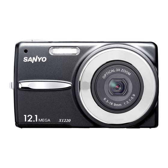
Digital Camera
Contents
1. OUTLINE OF CIRCUIT DESCRIPTION ............................... 3
2. DISASSEMBLY ................................................................... 10
3. ELECTRICAL ADJUSTMENT ............................................. 14
4. USB STORAGE INFORMATION REGISTRATION ............ 19
5. TROUBLESHOOTING GUIDE ............................................ 20
6. PARTS LIST ........................................................................ 22
RoHS
•This product does not contain any hazardous substances prohibited by the RoHS
Directive.
WARNING
•You are requested to use RoHS compliant parts for maintenance or repair.
•You are requested to use lead-free solder.
(This product has been manufactured using lead-free solder. Be sure to follow the
warning given on page 2 when carrying out repair work.)
CAUTION : Danger of explosion if battery is incorrectly replaced.
Replace only with the same or equivalent type recommended by the
manufacturer.
Discard used batteries according to the manufacturer's instructions.
NOTE : 1. Parts order must contain model number, part number, and description.
2. Substitute parts may be supplied as the service parts.
3. N. S. P. : Not available as service parts.
Design and specification are subject to change without notice.
SG41D/EX, GX, EX2, GX2, U3, PX, PX2 (R)
FILE NO.
VPC-X1220EX
(Product Code : 168 259 02)
(Europe) (U.K.) (South America)
(China) (Australia) (Hong Kong)
(Russia) (Middle East) (Africa)
(General) (Korea) (Taiwan)
VPC-X1220GX
(Product Code : 168 259 03)
(South America) (China)
(Australia) (Hong Kong)
(General) (Korea) (Taiwan)
VPC-X1220EXGD
(Product Code : 168 259 05)
(Europe) (U.K.) (South America)
(China) (Australia) (Hong Kong)
(Russia) (Middle East) (Africa)
(General) (Korea) (Taiwan)
VPC-X1220GXGD
(Product Code : 168 259 06)
(South America) (China)
(Australia) (Hong Kong)
(General) (Korea) (Taiwan)
VPC-X1250P
(Product Code : 168 259 07)
(U.S.A.) (Canada) (Taiwan) (General)
VPC-X1220PX
(Product Code : 168 259 10)
(Taiwan) (South America)
(General)
VPC-X1220PXGD
(Product Code : 168 259 11)
(Taiwan) (South America)
(General)
REFERENCE No. SM5310804
Advertisement
Chapters
Table of Contents

Related Manuals for Sanyo VPC-X1220EX


Summary of Contents for Sanyo VPC-X1220EX
-
Page 1: Table Of Contents
FILE NO. SERVICE MANUAL Digital Camera VPC-X1220EX (Product Code : 168 259 02) (Europe) (U.K.) (South America) (China) (Australia) (Hong Kong) (Russia) (Middle East) (Africa) (General) (Korea) (Taiwan) VPC-X1220GX (Product Code : 168 259 03) (South America) (China) (Australia) (Hong Kong) - Page 2 PRODUCT SAFETY NOTICE The components designated by a symbol ( ! ) in this schematic diagram designates components whose value are of special significance to product safety. Should any component designated by a symbol need to be replaced, use only the part designated in the Parts List.
-
Page 3: Outline Of Circuit Description
1. OUTLINE OF CIRCUIT DESCRIPTION 1-1. CCD CIRCUIT DESCRIPTION Pin 1 1. IC Configuration The CCD peripheral circuit block basically consists of the fol- lowing ICs. IC911 (RJ23Y3BA1LG) CCD imager IC901 (MAX8918ITM+T) V driver IC902 (AD9971BCPZRL) CDS, AGC, A/D converter, H driver, vertical TG Pin 21 2. - Page 4 3. IC901 (V Driver) 4. IC902 (H Driver, CDS, AGC and A/D converter) A V driver (IC901) is necessary in order to generate the clocks IC902 contains the functions of H driver, CDS, AGC and A/D (vertical transfer clock and electronic shutter clock) which converter.
- Page 5 1-2. CP1 CIRCUIT DESCRIPTION 1. Circuit Description 1-1. Signal processor 2. Outline of Operation 1. Gamma correction circuit When the shutter opens, the ASIC starts shooting operation. This circuit performs (gamma) correction in order to maintain When the TG/SG drives the CCD, picture data passes through a linear relationship between the light input to the camera the A/D and CDS, and is then input to the ASIC as the LVDS1.
- Page 6 4. Lens drive block 4-1. Zoom drive Drive settings are made by means of the serial data signals (L_STR, L_SCLK and L_SDATA) and data signal (ZIN) which are output by the ASIC (IC101). The motor drive signals (ZOUT+, and ZOUT-) are output in accordance with the set- tings from the motor driver IC (IC951) to drive the zoom DC motor.
- Page 7 5. Key Operaiton For details of the key operation, refer to the instruction manual. SCAN SCAN MENU PLAY SCENE LEFT RIGHT DOWN WIDE TELE PW_TEST TEST Table 2-1. Key Operation 6. Power Supply Control The ASIC controls the power supply for the overall system.The following is a description of how the power supply is turned on and off.
- Page 8 1-3. PWA POWER CIRCUIT DESCRIPTION 1. Outline 3. (CH1) Motor System 3.8 V Output This is the main power circuit, and is comprised of the follow- +3.8 V is output. BOOST 3.8 V output is so that PWM control ing blocks. can be carried out at the internal circuit of the switching con- Switching power controller (IC501) troller (IC501).
- Page 9 1-4. ST1 STROBE CIRCUIT DESCRIPTION 1. Charging Circuit 2. Light Emission Circuit When UNREG power is supplied to the charge circuit and the When FLCTL signal is input from the ASIC, the stroboscope CHG signal from microprocessor becomes High (3.3 V), the emits light.
-
Page 10: Disassembly
2. DISASSEMBLY 2-1. REMOVAL OF CABI BACK AND LCD 1. Screw 1.4 x 3 8. Screw 1.4 x 2 2. Screw 1.4 x 5 9. Three screws 1.4 x 4 3. Screw 1.4 x 5 10. Screw 1.6 x 5 4. - Page 11 2-2. REMOVAL OF CA1 BOARD, CP1 BOARD AND LENS 1. Spring BATT look 12. Spacer backup 2. Shaft CV BATT 13. Battery recharge 3. Spring open cover 14. CA1 board 4. Cover battery 15. Spacer lens 5. Cover DC 16. Adhesive backup 6.
- Page 12 2-3. REMOVAL OF ST1 BOARD AND ST2 BOARD 1. Earth USB 11. ST2 board 2. Four screws 1.4 x 3 12. Remove the solder. 3. Dec lens 13. Two screws 1.4 x 3.5 4. Cabi front 14. Remove the solder. 5.
- Page 13 2-4. BOARD LOCATION ST1 board CP1 board ST2 board – 13 –...
-
Page 14: Electrical Adjustment
URL. use and after power off for a while. http://www.overseas.sanyo.com/dcamera service/ Place the DscCalDi.exe file, camapi32.dll file and 3. Computer screen during adjustment QrCodeInfo.dll file together into a folder of your choice. - Page 15 3-6. The adjustment item which in necessary in part exchange CCD Black CCD White Lens Point And Point Factory Adjust- White Point Language storage Reset Defect Adjust- Cord Defect Detect Setting ment information Setting Detect Setting ment Adjustment registration (Infinity) Adjustment In Lighted COMPL PWB CP1...
- Page 16 PZ_SW_B_C: PZ2 Adjusting method: PZ2: adjustment value of zoom PR switch position 2 1. Set a distance of 0.5-1.0 cm between the pattern box and (1051<=PZ2+PBR<=1116) the camera when zoom wide edge. (Do not enter any light.) PZ_SW_C_B: PZ3 2. Double-click on the DscCalDi.exe. PZ3: adjustment value of zoom PR switch position 3 3.
- Page 17 3-9. Factory Code Setting 4. CCD Black Point And White Point Defect Detect Adjustment In Lighted 1. Check the "Factory Code" display within the Setting group. 2. For U.S.A., Canada and NTSC general area If "FC_SANYO_U" does not appear, click on the " "...
- Page 18 3-13. Firmware uploading procedure 1. Uploading the firmware should be carried out if the version number (COMPL PWB XX-X) on the replacement circuit board is lower than the version of the distributed firmware. For XX-X, enter the name of the circuit board containing the firmware.
-
Page 19: Usb Storage Information Registration
3. Click on the Get button in the USB storage window and check the USB storage data. VID: SANYO PID: X1250 (for VPC-X1250P) X1220 (for VPC-X1220EX, VPC-X1220GX, VPC-X1220EXGD, VPC-X1220GXGD, VPC-X1220PX and VPC-X1220PXGD) Serial: Rev. : 1.00 4. Check the “Serial” in the above USB storage data. If the... -
Page 20: Troubleshooting Guide
5. TROUBLESHOOTING GUIDE POWER LOSS INOPERTIVE TAKING INOPERATIVE PUSH SHUTTER PW SW ON BUTTON (S5302) (ON/OFF) IC501-B1 CHECK F5001 CHECK IC101 (BOOST 4.2 V) IC101-AB21 (S1) PUSH SHUTTER HIGH HALFWAY HIGH HIGH→LOW IC501-F6 CHECK S3502, CHECK IC501 (AL3.2 V) RB104 →... - Page 21 MEMO – 21 –...
-
Page 22: Parts List
LOCATION PARTS NO. DESCRIPTION LOCATION PARTS NO. DESCRIPTION 9101 636 132 8746 CARTON INNER-SG41D/EX Note: Refer to the table of accessories. VPC-X1220EX, VPC-X1220EXGD, VPC-X1220GX, 636 131 6033 STRAP -SG21F-M VPC-X1220GXGD, VPC-X1220PX, 636 133 2255 DISC,CD-ROM SSP G41D EX VPC-X1220PXGD Sanyo Software Pack(N.S.P.) - Page 23 Table of accessories...
- Page 24 CABINET AND CHASSIS PARTS 1 LOCATI O N PARTS NO. DESCRI P TI O N 636 132 5264 COVER_BATTERY-SG41D/U VPC-X1250, VPC-X1220EX, VPC-X1220GX, VPC-X1220PX 636 132 5271 COVER_BATTERY-SG41D/U2 VPC-X1250GD, VPC-X1220EXGD, VPC-X1220GXGD, VPC-X1220PXGD 636 133 4952 COVER_BATTERY-SG41D/U3 VPC-X1250P ONLY 636 121 9860...
- Page 25 CABINET AND CHASSIS PARTS 1 SG41D/J Parts List 1...
-
Page 26: Cabinet And Chassis Parts 2
636 121 9396 DEC_LENS-SG21F/U 636 139 4024 ASSY,CABI F-SV-SG41D/EX2 VPC-X1220EXGD, VPC-X1220GXGD, VPC-X1220PXGD 636 139 4000 ASSY,CABI F-SV-SG41D/EX VPC-X1220EX, VPC-X1220GX, VPC-X1220PX 636 136 1071 ASSY,CABI FRONT SV-SG41D VPC-X1250 ONLY 636 136 1019 ASSY,CABI FRONT SV-SG41D2 VPC-X1250GD ONLY 636 136 1125 ASSY,CABI FRONT SV-SG41D3... - Page 27 CABINET AND CHASSIS PARTS 2 SG41D/J Parts List 2...
-
Page 28: Electrical Parts
ELECTRICAL PARTS Note: 1. Materials of Capacitors and Resistors are abbreviated as follows ; Resistors Capacitors MT-FILM Metallized Film Resistor MT-POLYEST Metallized Polyester Capacitor MT-GLAZE Metallized Glaze Resistor MT-COMPO Metallized Composite Capacitor OXIDE-MT Oxide Metallized Film Resistor TA-SOLID Tantalum Solid Capacitor AL-SOLID Aluminum Solid Capacitor NP-ELECT... - Page 29 LOCATI O N PARTS NO. DESCRI P TI O N LOCATI O N PARTS NO. DESCRI P TI O N C1809 303 381 8109 CERAMIC 1U K 6.3V RB501 645 078 4613 R-NETWORK 2.2KX2 0.063W C1810 303 381 8109 CERAMIC 1U K 6.3V RB951 645 078 4835...
- Page 30 LOCATI O N PARTS NO. DESCRI P TI O N R9045 301 225 0500 MT-GLAZE 33K JA 1/16W R9047 301 225 1804 MT-GLAZE 47 JA 1/16W R9049 301 224 8804 MT-GLAZE 100 JA 1/16W R9053 301 225 0906 MT-GLAZE 82K JA 1/16W R9057 301 224 8903 MT-GLAZE 100K JA 1/16W...
-
Page 31: Circuit Diagrams & Printed Wiring Boards
CIRCUIT DIAGRAMS & PRINTED WIRING BOARDS TABLE OF CONTENTS OVERALL WIRING & BLOCK DIAGRAMS Page OVERALL WIRING .............................C3 OVERALL CIRCUIT ............................C4 CCD IMAGE SENSOR CIRCUIT........................C5 LENS CIRCUIT ..............................C5 MAIN CIRCUIT ..............................C6 POWER CIRCUIT ............................. C7 STROBE CIRCUIT .............................C7 CIRCUIT DIAGRAMS CIRCUIT WAVEFORMS .............................C7 CP1 BOARD (DMA) MAIN, LCD CONNECTOR &... - Page 32 NOTES: 1. All resistance values in "OHMS" unless otherwise noted. (K=1,000 ; M=1,000,000) 2. All capacitance values in "µF" unless otherwise noted. p=pico farad ; n=nano farad ; µ ,u or U=micro farad 3. All inductance values in "µH" unless otherwise noted. µ...
-
Page 33: Overall Wiring & Block Diagrams
OVERALL WIRING & BLOCK DIAGRAMS OVERALL WIRING LENS USB & AV BATTERY SPEAKER JW183 SP-/WT CN903 CN911 BACKUP_BAT BACKUP_BAT JW184 SP+/RD +14.5V(A) +14.5V(A) +14.5V(A) +14.5V(A) CCDOUT CCDOUT JW181 MIC/GY JW182 SUBGT2 SUBGT2 GND/BK SUBGT SUBGT -7.0V(A) -7.0V(A) -7.0V(A) -7.0V(A) CN102 CN541 V15B V15B... -
Page 34: Overall Circuit
OVERALL CIRCUIT CA1 BOARD PROGRAM FLASH CP1 BOARD CAA BLOCK SDRAM SD CARD PAON3 512Mbit/512Mbit SIO TO ASIC DATA1 CDS, AGC, LVDS DATA2 A/D C SG/TG H.DRIVER ADDRESS2 12M CCD ADDRESS1 V. DRIVER JPEG SDRAM CARD CONTROLLER USBD[+,-] CONTROLLER CONTROL BACKUP_BAT CLK. -
Page 35: Ccd Image Sensor Circuit
CCD IMAGE SENSOR CIRCUIT LENS CIRCUIT VDD3 +3.4V(A) CN951 LENS_BLOCK VDD3 IC903 PAON3 PAON3 -7.0V(A) +14.5V(A) +3.0V BOOST3.8V AL3.2V AFESD1P, AFESD1N 21, 31 14, 19 AFESD2P, AFESD2N LENS O_LPF LDOIN, LDOEN HVDD, DOUT0[P,N] AFECKP, AFECKN ZOOM_PR RGVDD DOUT1[P,N] Q9101 CCDINP CCDEN TCLK[P,N] CCDSD... -
Page 36: Main Circuit
MAIN CIRCUIT ST1 BOARD STROBE CAPACITOR IC541 300V 80µF STROBE SHUTTER_SW CHARGE S3502 D3501 SELF_LED POWER_SW S3501 Xe TUBE CP1 BOARD Li-ion 3.7V PWA BLOCK UNREGST UNREGSY 32.768KHz X5001 D1001 BACK UNIT FPC IC506 VDD1.8 VDD3 IC501 Q1009 Q1008 BOOST3.8V SWITCHING A_VDD1.8 WIDE... -
Page 37: Power Circuit
CIRCUIT DIAGRAMS POWER CIRCUIT CIRCUIT WAVEFORMS TEST POINT TEST POINT VOUT1[A,B] WAVEFORM WAVEFORM LOCATION LOCATION VIN8 L5301 BOOST3.8V SW1[A,B,C,D] STEP UP CIRCUIT IC101 CN171 PIN A3 PIN 7 L5041,D5041 +14.5V(A) STEP UP CIRCUIT DCLK L5051,D5051 1V/div 1V/div -7.0V(A) INVERTING CIRCUIT 10ns/div 20ns/div VOUT8... -
Page 38: Cp1 Board (Dma) Main, Lcd Connector & Lens
CP1 BOARD (DMA) MAIN, LCD CONNECTOR & LENS R1001 A_VDD3 AL3.2V 0;1/16Z VDD3 A_VDD3 DMA(MAIN) R1002 C1034 0.1;B A_VDD1.8 DMA(LENS) 0;1/16Z A_VDD1.8 VDD1.8 R1003 A_VDD1.1 0;1/16Z A_VDD1.1 VDD1.1 D1-25900/SG41D-U R1121 1.2K;1/16D AL3.2V VOLTAGE: VIEW MODE, LCD ON MRST R1122 ZMRST 1M;1/16J XOUT D4CKI... - Page 39 CP1 BOARD (DMA) MAIN, LCD CONNECTOR & LENS [UPPER-LEFT] R1001 A_VDD3 AL3.2V 0;1/16Z A_VDD3 VDD3 DMA(MAIN) C1034 0.1;B R1002 A_VDD1.8 0;1/16Z A_VDD1.8 VDD1.8 R1003 A_VDD1.1 0;1/16Z A_VDD1.1 VDD1.1 D1-25900/SG41D-U R1121 1.2K;1/16D AL3.2V VOLTAGE: VIEW MODE, LCD ON MRST R1122 ZMRST 1M;1/16J XOUT D4CKI...
- Page 40 CP1 BOARD (DMA) MAIN, LCD CONNECTOR & LENS [UPPER-RIGHT] AL3.2V C1034 0.1;B DMA(LENS) VDD3 CN951 FOUT_A- LD_motor_A- FOUT_B+ LD_motor_B+ FOUT_B- LD_motor_B- FOUT_A+ LD_motor_A+ BOOST3.8V FPI_C LD_PI_C GNDP3 FPI_K RB952 LD_PI_EK VDD11P3 C9503 LD_PI_A GNDP2 0.1;B SCLK Zoom_PI_A VDD11P2 E3 INPUT4 ZPI_C FOUT_B- ZPR_K...
- Page 41 CCDEN DQ29 CCDSD DQ28 CCDSD DQ28 I2C_SDA DQ27 GPIOB[0] DQ27 TGVD I2C_SCL DQ26 TGVD GPIOB[1] DQ26 TGHD RXD0 DQ25 TGHD GPIOB[2] DQ25 TXD0 DQ24 GPIOB[3] DQ24 SUBGT SDDAT0 DQ23 SUBGT GPIOC[0] CP1 BOARD (DMA) MAIN, LCD CONNECTOR & LENS [LOWER-LEFT] DQ23 SUBGT2 SDDAT1...
- Page 42 AGND DQ29 VOUT DQ28 C1730 DQ28 4.7;B 10 DQ27 1608 COMDC DQ27 QXC61GN2902HP DQ26 VCAC DQ26 XC61GN2902HR IC302 DQ25 DQ25 VOLTAGE DET. DQ24 BAT_OFF VLED DQ24 LCDAN DQ23 DQ23 CP1 BOARD (DMA) MAIN, LCD CONNECTOR & LENS [LOWER-RIGHT] LCDCA DQ22 VCOM DQ22 DQ21...
-
Page 43: Cp1 Board (Pwa) Power
CP1 BOARD (PWA) POWER LITTELFUSE 1608 F5002 2A32V CL502 BAT+ UNREGST CL504 BATT BATTEMP UNREGSY TO DMA 2A32V F5001 1608 CL503 LITTELFUSE BAT- TO BATTERY R5043 R5096 2.2;1/16J 0;1/16Z +14.5V(A) P1-25900/SG41D-U VOLTAGE: VIEW MODE, LCD ON (USE BATTERY) R5097 0;1/16Z -7.0V(A) 1AV4L26B5580G L5041... -
Page 44: Cp1 Board (Caa) Ccd Afe & Driver
CP1 BOARD (CAA) CCD AFE & DRIVER BACKUP_BAT BACKUP_BAT CCDVL CCDVH VDRST RESETB CCDVL VDRST SCLK VDRST SCLK CCDVM2 CN903 SCLK SAV2 SCLK SAV2 CCDVM1 IC901 SAV1 SAV2 BACKUP_BAT SAV2 SAV1 MAX8918ITM+T OV10 BACKUP_BAT SAV0 V15C SAV1 QMAX8918ITM+P SAV1 SAV0 OV11 SAV0 SDV5... -
Page 45: Ca1 Board Ccd Image Sensor
CA1 BOARD CCD IMAGE SENSOR CN911 BACKUP_BAT UT414-TZ1 Z9101 +14.5V(A) +14.5V(A) CCDOUT -0.7 -0.7 SUBGT2 SUBGT2 -5.0 -0.7 -5.0 -1.4 -5.4 -5.6 SUBGT SUBGT V13B V15A V13B V15A R9102 V13A V15B -1.0 470;1/16J V13A V15B 14.6 -0.7 -0.7 R9104 -0.7 -7.0V(A) 47;1/16J -6.1... -
Page 46: St1 Board Strobe & Switch
ST1 BOARD STROBE & SWITCH STROBE UNIT 1AV4L17B0620G T5401 JW541 AWG32/AWG30 TTRN-0530H-018-T BROWN D5402 2.0X1.25 RE0208DA PINK C5410 0.022;350B 3216 1AV4L17B0450N T5402 TS-F35A-3 D3501 R3506 CN541 SML-E12U8WG 270;1/16J SELF_LED AL3.2V CHGDONE JW542 AWG32/AWG30 FLCTL STROBE BLACK CHARGE 2.0X1.25 RB541 PW_ON 1KX4 1/16W IC541 BD4221NUX... -
Page 47: Printed Wiring Boards (P.w.b.)
PRINTED WIRING BOARDS (P.W.B.) CP1 P.W.B. (SIDE A) CP1 P.W.B. (SIDE B) R5083 C5083 R5082 C5082 CL303 CL191 CL520 CL509 CL525 C5302 R5081 C9018 C9008 C9007 R5096 C3001 CL524 C9032 R9044 CL507 CL510 CL508 R5041 F5002 F5001 C9030 C5303 L9001 CL526 R5094 C5043... -
Page 48: Ca1 P.w.b. (Side A & B)
CA1 P.W.B. (SIDE A) CA1 P.W.B. (SIDE B) Z9101 R9104 ST1 P.W.B. (SIDE A) ST1 P.W.B. (SIDE A) CL548 CL554 SIDE-A CL542 CL545 CL544 R5422 R5416 CL547 CL541 CL549 C5413 C5414 C5410 R5417 SIDE-B S3502 R5415 S3501 R5414 R5413 J9000AA CL553 T5401 CL546... - Page 49 SANYO Electric Co., Ltd. Osaka, Japan Nov./’09...