Yamaha RX-V550 Service Manual
Yamaha av receiver/av amplifier service manual
Hide thumbs
Also See for RX-V550:
- Service manual (125 pages) ,
- Owner's manual (79 pages) ,
- Supplementary manual (40 pages)
Advertisement
RX-V450/HTR-5740/DSP-AX450
This manual has been provided for the use of authorized YAMAHA Retailers and their service personnel.
It has been assumed that basic service procedures inherent to the industry, and more specifically YAMAHA Products, are already
known and understood by the users, and have therefore not been restated.
WARNING:
IMPORTANT:
The data provided is believed to be accurate and applicable to the unit(s) indicated on the cover. The research, engineering, and
service departments of YAMAHA are continually striving to improve YAMAHA products. Modifications are, therefore, inevitable
and specifications are subject to change without notice or obligation to retrofit. Should any discrepancy appear to exist, please
contact the distributor's Service Division.
WARNING:
IMPORTANT:
I CONTENTS
TO SERVICE PERSONNEL .......................................... 2
IMPEDANCE SELECTOR ............................................. 3
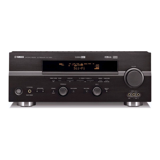
FRONT PANELS ........................................................ 4~6
REAR PANELS ........................................................ 7~15
REMOTE CONTROL PANELS .................................... 16
INTERNAL VIEW ......................................................... 18
SELF DIAGNOSIS FUNCTION (DIAG)
1 0 0 8 8 4
AV RECEIVER/AV AMPLIFIER
RX-V550/HTR-5750
IMPORTANT NOTICE
Failure to follow appropriate service and safety procedures when servicing this product may result in personal
injury, destruction of expensive components, and failure of the product to perform as specified. For these reasons,
we advise all YAMAHA product owners that any service required should be performed by an authorized
YAMAHA Retailer or the appointed service representative.
The presentation or sale of this manual to any individual or firm does not constitute authorization, certification or
recognition of any applicable technical capabilities, or establish a principle-agent relationship of any form.
Static discharges can destroy expensive components. Discharge any static electricity your body may have
accumulated by grounding yourself to the ground buss in the unit (heavy gauge black wires connect to this buss).
Turn the unit OFF during disassembly and part replacement. Recheck all work before you apply power to the unit.
17~18
......... 19~21
22~42
SERVICE MANUAL
IC DATA ................................................................. 44~49
BLOCK DIAGRAM ................................................. 50~51
DISPLAY DATA ........................................................... 52
PRINTED CIRCUIT BOARD .................................. 53~73
PIN CONNECTION DIAGRAM .................................... 74
SCHEMATIC DIAGRAM ........................................ 75~85
PARTS LIST ......................................................... 87~123
REMOTE CONTROL .......................................... 124~125
43
P.O.Box 1, Hamamatsu, Japan
Advertisement
Table of Contents

Related Manuals for Yamaha RX-V550


Summary of Contents for Yamaha RX-V550
-
Page 1: Table Of Contents
This manual has been provided for the use of authorized YAMAHA Retailers and their service personnel. It has been assumed that basic service procedures inherent to the industry, and more specifically YAMAHA Products, are already known and understood by the users, and have therefore not been restated. -
Page 2: Remote Control Panels
RX-V550/HTR-5750 RX-V450/HTR-5740/DSP-AX450 I REMOTE CONTROL PANELS RX-V550 (U, C, A, L, R, T, K models) RX-V550 (B, G, E models) RX-V450 (B, G, E models) HTR-5750 (U, C, A, T, K models) HTR-5740 (G, E models) RX-V450 (U, C, A, L, R, T, K models) -
Page 3: Specifications
Component Video Signal Level 5 Hz to 60 MHz, -3 dB Finish [RX-V450/HTR-5740] [RX-V550/HTR-5750/DSP-AX450] RX-V550 ......Gold color (L, R, T, K) models Composite Video Signal Level 5 Hz to 10 MHz, -3 dB FRONT L/R (8/6/4/2 ohms) 115/150/185/230 W... -
Page 4: Internal View
7 FUNCTION (3) P.C.B. (HTR-5750, DSP-AX450 only) DELEY : 0 ms 0 ms to 160 ms / 1 step 8 FUNCTION (4) P.C.B. ( Except RX-V550 ) DUAL MONO : MAIN [MAIN] / SUB / ALL 9 FUNCTION (8) P.C.B. -
Page 5: Disassembly Procedures
RX-V550/HTR-5750 RX-V450/HTR-5740/DSP-AX450 RX-V550 I DISASSEMBLY PROCEDURES (Remove parts in the order as numbered.) Disconnect the power cable from the AC outlet. 1. Removal of Top Cover 4. Removal of Sub Chassis Unit a. Remove 2 screws (5) and then slide the Sub Chassis Unit a. - Page 6 RX-V550/HTR-5750 RX-V450/HTR-5740/DSP-AX450 HTR-5750 RX-V450/HTR-5740/DSP-AX450 7. Removal of MAIN (1), MAIN (5), MAIN (7) and I DISASSEMBLY PROCEDURES POWER (1) P.C.B.s a. Remove CB351, CB354 and CB503. (Fig. 5) (Remove parts in the order as numbered.) b. Remove 2 screws (9), 2 screws (0) and 3 screws (A).
- Page 7 RX-V550/HTR-5750 RX-V450/HTR-5740/DSP-AX450 HTR-5750/RX-V450/HTR-5740 DSP-AX450 5. Removal of MAIN (1), MAIN (5), MAIN (7) and POWER (1) P.C.B.s a. Remove CB351, CB354 and CB503. (Fig. 5) b. Remove 2 screws (7), 2 screws (8) and 3 screws (9). (Fig. 5) c. Remove MAIN (1), MAIN (5), MAIN (7) and POWER (1) P.C.B.s..
- Page 8 RX-V550/HTR-5750 RX-V450/HTR-5740/DSP-AX450 I SELF DIAGNOSIS FUNCTION (DIAG) This unit has self diagnosis functions that are intended for inspection, measurement and location of faulty point. There are 17 DIAG menu items, each of which has sub- menu items. No DIAG menu...
- Page 9 RX-V550/HTR-5750 RX-V450/HTR-5740/DSP-AX450 • Starting DIAG Press the “STANDBY/ON” key while simultaneously pressing those two keys of the main unit as indicated in the figure below. Keys of main unit Turn on the power while pressing these keys. • Starting DIAG in the protection cancel...
- Page 10 RX-V550/HTR-5750 RX-V450/HTR-5740/DSP-AX450 • Display provided when DIAG started The FL display of the main unit displays the protection function history data and the version (1 alphabet) and the DIAG menu [sub-menu (YSS MARGIN) of DIAG menu No.1 DSP THROUGH] a few seconds later.
- Page 11 RX-V550/HTR-5750 RX-V450/HTR-5740/DSP-AX450 When there is a history of protection Version (1 alphabet) function due to abnormal DC output Cause: DC output of the power amplifier is abnormal. Supplementary information: The abnormal voltage is displayed in % based on 5V as 100%.
- Page 12 RX-V550/HTR-5750 RX-V450/HTR-5740/DSP-AX450 • Operation procedure of DIAG menu and SUB-MENU There are 17 MENU items, each of which has some SUB- MENU items. DIAG menu selection Main unit: Select the menu using the PROGRAM knob. SUB-MENU selection Main unit: Select the sub-menu using (Forward) and (Reverse) keys of PRESET/TUNING.
- Page 13 RX-V550/HTR-5750 RX-V450/HTR-5740/DSP-AX450 • Details of DIAG menu With full-bit output specified in some modes, it is possible to execute 0dBFS output without head margin in each channel. 1. DSP THROUGH YSS MARGIN • The front CH signal including the head margin is output at the main CH.
- Page 14 RX-V550/HTR-5750 RX-V450/HTR-5740/DSP-AX450 2. BYPASS ANALOG BYPASS • The signal for L/R is output as it is without passing through the DSP section. Reference data INPUT: DVD ANALOG SWFR: 50Hz, Others: 1kHz SPEAKER OUTPUT (1kHz) SUBWOOFER Input level Volume FRONT L/R...
- Page 15 RX-V550/HTR-5750 RX-V450/HTR-5740/DSP-AX450 3. RAM THROUGH Using the sub-menu, it is possible to select the full-bit output at 0dB output level. When ANALOG and PCM are selected, signals are distributed to each channel by YSS930. RAM MARGIN Reference data INPUT: DVD ANALOG...
- Page 16 RX-V550/HTR-5750 RX-V450/HTR-5740/DSP-AX450 4. PRO LOGIC It is possible to select PRO LOGIC I, II (Movie) or Meo:6 by using the sub-menu. When PRO LOGIC I or II (Movie) is selected, Auto Input Balance is always turned off. PRO LOGIC I...
- Page 17 RX-V550/HTR-5750 RX-V450/HTR-5740/DSP-AX450 Neo:6 Reference data INPUT: DVD ANALOG SWFR: 50Hz, Others: 1kHz SPEAKER OUTPUT (1kHz) SUBWOOFER Input level Volume FRONT L/R CENTER SURROUND L/R SURROUND BACK OUTPUT (50Hz) - ∞ - ∞ - ∞ ∞ Each ch, -20 dBm +6.0 dB +13.0 dBm...
- Page 18 RX-V550/HTR-5750 RX-V450/HTR-5740/DSP-AX450 5. SPEAKERS SET The input signal is automatically identified and switched in the priority order of dts → DOLBY DIGITAL → AAC → PCM AUDIO → Analog (A/D) according to the signal detection. The signals output from the DSP block are the same as 2.
- Page 19 RX-V550/HTR-5750 RX-V450/HTR-5740/DSP-AX450 6. EXTERNAL INPUT The signal input through the 6CH INPUT terminals is output. The speaker impedance can be selected. 6ch INPUT_6 Reference data INPUT: 6CH INPUT SWFR: 50Hz, Others: 1kHz SPEAKER OUTPUT (1kHz) SUBWOOFER Input level Volume FRONT L/R...
- Page 20 RX-V550/HTR-5750 RX-V450/HTR-5740/DSP-AX450 8. DISPLAY CHECK This program is used to check the FL display section. The display condition varies as shown below according to the sub-menu operation. The signals are processed using EFFECT OFF (The L/R signal is output using ANALOG MAIN BYPASS.)
- Page 21 RX-V550/HTR-5750 RX-V450/HTR-5740/DSP-AX450 9. MANUAL TEST The noise generator circuit built into the DSP outputs the test noise through the channels specified by the sub- menu. The noise frequency for LFE is 35 to 250 Hz. Other than that, the center frequency is 800Hz.
- Page 22 RX-V550/HTR-5750 RX-V450/HTR-5740/DSP-AX450 • PRESET STATIONS / STATION FM FACTORY PRESET DATA (MHz) STATION AM FACTORY PRESET DATA (kHz) PAGE NO. U, C R, T, K, A, B, G, L PAGE NO. U, C, R, T, K A, B, G, L 87.5...
- Page 23 RX-V550/HTR-5750 RX-V450/HTR-5740/DSP-AX450 REC-OUT Not applied to these models. IMP SW/POWER LIMIT (Impedance/power limiter detection) IMP: Not applied to these models. PL: Power limiter detection value The voltage value of pin No. 92 of IC502 is displayed, using 5V/256 as standard.
- Page 24 RX-V550/HTR-5750 RX-V450/HTR-5740/DSP-AX450 13. IF STATUS (Input function status) Using the sub-menu, the status data is displayed one after another in the hexadecimal notation. During signal processing, the status before execution of this menu is maintained. * The numeric value in the figure is an example for reference.
- Page 25 RX-V550/HTR-5750 RX-V450/HTR-5740/DSP-AX450 <5th byte> Signal processing status information *2: With digital signals other than 32kHz, 44.1kHz and 48kHz, through processing method is used for reproducible signals. bit7 MUTE request bit3 – bit6 Red dts flashing bit2 Through & bypass (*2) bit5 6.1/EX processing...
- Page 26 RX-V550/HTR-5750 RX-V450/HTR-5740/DSP-AX450 14. DSP RAM CHECK This menu is used to self-diagnose whether or not the bus connection for the YSS930 and the external RAM is made properly. During signal processing, the status before execution of this menu is maintained.
- Page 27 RX-V550/HTR-5750 RX-V450/HTR-5740/DSP-AX450 16. SOFT SW This menu is used to switch the function settings on P.C.B. through the software so as to activate the product. The protection function follows the P.C.B. settings. When connected to AC or in the maker preset state, the unit is initialized to the P.C.
- Page 28 RX-V550/HTR-5750 RX-V450/HTR-5740/DSP-AX450 17. MICROPROCESSOR INFORMATION There are 4 sub-menu items. The version, checksum and the port specified by the microprocessor are displayed. The signal is processed using EFFECT OFF. The checksum is obtained by adding the data at every 16 bits for each program area and expressing the result as a 4-figure hexadecimal data.
-
Page 29: Amp Adjustment
RX-V550/HTR-5750 RX-V450/HTR-5740/DSP-AX450 I AMP ADJUSTMENT Confirmation of Idling Current of MAIN (1) P. C. B. • Right after power is turned on, confirm that each measured voltage across the terminals of R45 (Front Lch), R46 (Front Rch), R50 (Center), R47 (Surround Lch), R48 (Surround Rch), R49 (Surround Back) is between 0.1mV and 10.0mV. -
Page 30: Ic Data
RX-V550/HTR-5750 RX-V450/HTR-5740/DSP-AX450 I IC DATA IC5 : YSS948 (DSP P.C.B.) DSP (Main Decoder) AHVSS VDD2 AHVSSG VDD2 DVSS DVDD VDD2 MEMD7 VDD2 MEMD6 MEMD5 MEMD4 VDD1 VDD1 STATUS4 MEMD3 STATUS5 MEMD2 STATUS6 MEMD1 STATUS7 MEMD0 VDD2 VDD2 TEST TEST MEMA0... - Page 31 RX-V550/HTR-5750 RX-V450/HTR-5740/DSP-AX450 IC5 : YSS948 (DSP P.C.B.) IC5 : YSS948 (DSP P.C.B.) DSP (Main Decoder) DSP (Main Decoder) Terminal Output Terminal Output Function Function Category Pin No. Category Pin No. name Note 1) current name Note 1) current Power supply VDD1 –...
- Page 32 RX-V550/HTR-5750 RX-V450/HTR-5740/DSP-AX450 IC5 : YSS948 (DSP P.C.B.) IC7 : YSS930-SZ (DSP P.C.B.) DSP (Main Decoder) DSP (Post Processor) Terminal Output Function Category Pin No. name Note 1) current External MEMD7 External memory data input/output terminals 7 to 0 VDD2 memory...
- Page 33 RX-V550/HTR-5750 RX-V450/HTR-5740/DSP-AX450 IC7 : YSS930-SZ (DSP P.C.B.) IC7 : YSS930-SZ (DSP P.C.B.) DSP (Post Processor) DSP (Post Processor) Name Function Name Function Digital ground terminal Data input/output terminal 14 for external memory Terminal for connecting crystal oscillator Data input/output terminal 15 for external memory...
- Page 34 Oscillation output 56 P36/A14 CMP1 Compornent Selector 1 COMP 14 Vss Ground for microprocessor 57 P35/A13 TRIG Trigger control Remote (RX-V550 only) 15 Xin Oscillation input 16MHz 58 P34/A12 N.C. 16 Vcc Power supply for microprocessor +5V Vcc(BU) 59 P33/A11 RDSE...
- Page 35 INPUT SEL. Rotary B check 86 P02/D2 TONEA Tone Con. Rotary A (RX-V550 only) Remitter presence check 0, 1 UC At reset cancellation and at power ON, switched to input in an instant 87 P01/D1 TONEB Tone Con. Rotary B...
-
Page 36: Block Diagram
IC801 VOLUME IC16 1/2 XL501 ZONE2 SELECTOR • See page 75 → RX-V550 U, C, A models only SCHEMATIC DIAGRAM 16MHz OPERATION FUNCTION (1) • See page 76, 78 → SCHEMATIC DIAGRAM • See page 80, 81 → SCHEMATIC DIAGRAM... -
Page 37: Schematic Diagram
RX-V550/HTR-5750 RX-V450/HTR-5740/DSP-AX450 I BLOCK DIAGRAM (2/2) • See page 82 → SCHEMATIC DIAGRAM SUB TRANS MAIN RX-V550, HTR-5750, DSP-AX450 only • See page 84 → SCHEMATIC DIAGRAM 8ohm/4ohm /4ohm IC1-4 C-INPUT IC603 Q604 SELECTOR RY401 IC608 T401 IC601 D-TV/CBL S-MONITOR... - Page 38 RX-V550/HTR-5750 RX-V450/HTR-5740/DSP-AX450 G ANODE CONNECTION I DISPLAY DATA 9G~5G G V801 : 16-BT-122GNK (WC173100) PATTERN AREA G PIN CONNECTION Pin No. Connection Pin No. Connection Note : 1) F1, F2 ..Filament 2) NP ..No pin 3) NX ..No extened 4) DL ..
- Page 39 RX-V550/HTR-5750 RX-V450/HTR-5740/DSP-AX450 I PIN CONNECTION DIAGRAM • ICs • Diodes 1N4002S MTZJ10B 1SS355 SB01-05Q µPC29M33T-E1 LM61CIZ NJU7201L55 NJM7805FA NJM79M05FA PQ025EZ5MZP NJM2068MD 1SS133 MTZJ15A MA8051-M Anode NJM7812FA NJM79M12FA PQ012FZ01ZP NJM2904M 1SS176 MTZJ2.4B MA8056-M Anode TK15420M 1SS244 MTZJ3.0A MA8075-H µPC4570G2 1SS270A MTZJ6.8B MA8091-M MTZJ9.1B...
- Page 40 RX-V550/HTR-5750/RX-V450/HTR-5740/DSP-AX450 SCHEMATIC DIAGRAM (DSP) RX-V550: Page 77 RX-V550: Page 76 IC8: MSM514260E-60JS HTR-5750, RX-V450, HTR-5740, DSP-AX450: Page 79 HTR-5750, RX-V450, HTR-5740, DSP-AX450: Page 78 RX-V550/HTR-5750 4Mbit DRAM Reference No. U, C, R, T, K, A, B, G, L, E memo...
- Page 41 RX-V550/HTR-5750/RX-V450/HTR-5740/DSP-AX450 SCHEMATIC DIAGRAM (FUNCTION 1/2) RX-V550 Page 77 Page 75 Page 80 to FUNCTION (2) to DSP to OPERATION (4) HP AMP. MUTE 10.0 x: NOT USED O:USED / APPLICABLE Page 80 to OPERATION (1) 11.8 -9.2 -9.8 -9.2 -11.7 FRONT L 11.8...
- Page 42 RX-V550/HTR-5750/RX-V450/HTR-5740/DSP-AX450 SCHEMATIC DIAGRAM (FUNCTION 2/2) RX-V550 Point 1 Pin 13 of IC502 Point 2 Cathode of D501 and Pin 12 of IC502 A D501 B IC502 POWER ON POWER OFF -4.9 (Connect the power cable) (Disconnect the power cable) x: NOT USED...
- Page 43 RX-V550/HTR-5750/RX-V450/HTR-5740/DSP-AX450 SCHEMATIC DIAGRAM (FUNCTION 1/2) HTR-5750 RX-V450/HTR-5740/DSP-AX450 Page 79 Page 75 Page 81 to FUNCTION (2) to DSP to OPERATION (4) HP AMP. MUTE 10.0 Page 81 to OPERATION (1) 11.8 -9.2 -9.8 -9.2 -11.7 FRONT L 11.8 Page 83 -11.6...
- Page 44 RX-V550/HTR-5750/RX-V450/HTR-5740/DSP-AX450 SCHEMATIC DIAGRAM (FUNCTION 2/2) HTR-5750 RX-V450/HTR-5740/DSP-AX450 HTR-5750 IC501: NJU7201L55 Point 1 Pin 13 of IC502 Point 2 Cathode of D501 and Pin 12 of IC502 R549 100K 100K 100K Voltage Regulator RD35810 RD35810 RD35810 R553 100K RD35810 R552 100K...
- Page 45 RX-V550/HTR-5750/RX-V450/HTR-5740/DSP-AX450 SCHEMATIC DIAGRAM (OPERATION) RX-V550 FL DISPLAY to Power Transformer -20.8 -18.2 -20.3 -26.0 -24.1 -22.0 -22.1 -22.5 FL DRIVER -26.0 -22.1 -22.0 -22.1 -24.1 -24.1 -18.2 -22.5 -18.2 -18.2 -24.0 -18.1 -16.0 -22.0 -20.1 -22.1 Page 76 to FUNCTION (1) -26.0...
- Page 46 RX-V550/HTR-5750/RX-V450/HTR-5740/DSP-AX450 SCHEMATIC DIAGRAM (OPERATION) HTR-5750 RX-V450/HTR-5740/DSP-AX450 FL DISPLAY IC801: M66003-0101FP FL Display Driver Display code CGROM (35 bit x 166) SEG00 (8-bit x 60) Segment SEG25 Code output write SEG26 circuit CGROM Serial dot data SEG34 data (35 bit x 16)
- Page 47 RX-V550/HTR-5750/RX-V450/HTR-5740/DSP-AX450 SCHEMATIC DIAGRAM (MAIN) RX-V550: Page 77 55.3 55.2 Page 83 55.3 HTR-5750, RX-V450, HTR-5740, to POWER (1) 55.3 DSP-AX450: Page 79 to FUNCTION (2) -0.4 55.0 -1.0 -0.5 -0.5 -1.0 -0.5 -52.8 -1.0 -55.2 -55.2 -55.3 -53.3 -53.9 55.3 55.3...
- Page 48 RX-V550/HTR-5750/RX-V450/HTR-5740/DSP-AX450 SCHEMATIC DIAGRAM (POWER) 19.1 AC30.4 -0.1 -0.1 11.8 19.1 11.2 11.2 -20.0 to Power Transformer AC18.3 POWER AMP. 11.2 54.0 -11.9 53.5 -11.7 -20.0 -4.9 -11.9 FRONT L 54.6 53.5 -0.6 -0.6 Page 82 to MAIN (1) IC301: LM61CIZ...
- Page 49 RX-V550/HTR-5750/RX-V450/HTR-5740/DSP-AX450 SCHEMATIC DIAGRAM (SUBTRANS) to POWER (2) R, L models Page 83 Other models to Power Transformer -0.2 AC88.9 RESET x: NOT USED O: USED / APPLICABLE AC8.1 POWER DETECT IC402: TC4013BP Dual D-type Flip Flop RESET1 SET1 DATA1 CLOCK1...
- Page 50 RX-V550/HTR-5750/RX-V450/HTR-5740/DSP-AX450 SCHEMATIC DIAGRAM (VIDEO) DSP-AX450 Page 79 to FUNCTION (2) IC851, 852: TC74HC4053AF Analog Multiplexer/Demultiplexer INHIBIT INPUT STATES "ON" CHANNNEL (S) LEVEL BINARY TO 1-OF-8 INHIBIT CONVERTER DECODER WITH INHIBIT 0X, 0Y, 0Z 1X, 0Y, 0Z 0X, 1Y, 0Z 1X, 1Y, 0Z...
-
Page 51: Parts List
RX-V550/HTR-5750 RX-V450/HTR-5740/DSP-AX450 PARTS LIST I ELECTRICAL PARTS I WARNING Components having special characteristics are marked s and must be replaced with parts having specifications equal to those originally installed. ABBREVIATIONS IN THIS LIST ARE AS FOLLOWS: C.A.EL.CHP : CHIP ALUMI.ELECTROLYTIC CAP L.EMIT... - Page 52 RX-V550/HTR-5750 RX-V450/HTR-5740/DSP-AX450 P.C.B. DSP ✻ New Parts...
- Page 53 RX-V550/HTR-5750 RX-V450/HTR-5740/DSP-AX450 P.C.B. DSP ✻ New Parts...
- Page 54 RX-V550/HTR-5750 RX-V450/HTR-5740/DSP-AX450 RX-V550 P.C.B. DSP & P.C.B. FUNCTION ✻ New Parts...
- Page 55 RX-V550/HTR-5750 RX-V450/HTR-5740/DSP-AX450 RX-V550 P.C.B. FUNCTION ✻ New Parts...
- Page 56 RX-V550/HTR-5750 RX-V450/HTR-5740/DSP-AX450 RX-V550 P.C.B. FUNCTION ✻ New Parts...
- Page 57 RX-V550/HTR-5750 RX-V450/HTR-5740/DSP-AX450 RX-V550 P.C.B. FUNCTION ✻ New Parts...
- Page 58 RX-V550/HTR-5750 RX-V450/HTR-5740/DSP-AX450 RX-V550 P.C.B. FUNCTION ✻ New Parts...
- Page 59 RX-V550/HTR-5750 RX-V450/HTR-5740/DSP-AX450 RX-V550 P.C.B. FUNCTION ✻ New Parts...
- Page 60 RX-V550/HTR-5750 RX-V450/HTR-5740/DSP-AX450 HTR-5750 RX-V450/HTR-5740/DSP-AX450 P.C.B. FUNCTION ✻ New Parts...
- Page 61 RX-V550/HTR-5750 RX-V450/HTR-5740/DSP-AX450 HTR-5750 RX-V450/HTR-5740/DSP-AX450 P.C.B. FUNCTION ✻ New Parts...
- Page 62 RX-V550/HTR-5750 RX-V450/HTR-5740/DSP-AX450 HTR-5750 RX-V450/HTR-5740/DSP-AX450 P.C.B. FUNCTION ✻ New Parts...
- Page 63 RX-V550/HTR-5750 RX-V450/HTR-5740/DSP-AX450 HTR-5750 RX-V450/HTR-5740/DSP-AX450 P.C.B. FUNCTION ✻ New Parts...
- Page 64 RX-V550/HTR-5750 RX-V450/HTR-5740/DSP-AX450 HTR-5750 RX-V450/HTR-5740/DSP-AX450 P.C.B. FUNCTION ✻ New Parts...
- Page 65 RX-V550/HTR-5750 RX-V450/HTR-5740/DSP-AX450 HTR-5750 RX-V450/HTR-5740/DSP-AX450 RX-V550 P.C.B. FUNCTION & P.C.B. OPERATION ✻ New Parts...
- Page 66 RX-V550/HTR-5750 RX-V450/HTR-5740/DSP-AX450 RX-V550 HTR-5750 RX-V450/HTR-5740/DSP-AX450 P.C.B. OPERATION ✻ New Parts...
- Page 67 RX-V550/HTR-5750 RX-V450/HTR-5740/DSP-AX450 HTR-5750 RX-V450/HTR-5740/DSP-AX450 P.C.B. OPERATION ✻ New Parts...
- Page 68 RX-V550/HTR-5750 RX-V450/HTR-5740/DSP-AX450 P.C.B. MAIN ✻ New Parts...
- Page 69 RX-V550/HTR-5750 RX-V450/HTR-5740/DSP-AX450 P.C.B. MAIN ✻ New Parts...
- Page 70 RX-V550/HTR-5750 RX-V450/HTR-5740/DSP-AX450 P.C.B. MAIN ✻ New Parts...
- Page 71 RX-V550/HTR-5750 RX-V450/HTR-5740/DSP-AX450 P.C.B. MAIN ✻ New Parts...
- Page 72 RX-V550/HTR-5750 RX-V450/HTR-5740/DSP-AX450 P.C.B. MAIN ✻ New Parts...
- Page 73 RX-V550/HTR-5750 RX-V450/HTR-5740/DSP-AX450 P.C.B. MAIN ✻ New Parts...
- Page 74 RX-V550/HTR-5750 RX-V450/HTR-5740/DSP-AX450 P.C.B. POWER ✻ New Parts...
- Page 75 RX-V550/HTR-5750 RX-V450/HTR-5740/DSP-AX450 P.C.B. POWER ✻ New Parts...
- Page 76 RX-V550/HTR-5750 RX-V450/HTR-5740/DSP-AX450 P.C.B. POWER & P.C.B. SUBTRANS ✻ New Parts...
- Page 77 RX-V550/HTR-5750 RX-V450/HTR-5740/DSP-AX450 RX-V550 HTR-5750 RX-V450/HTR-5740/DSP-AX450 DSP-AX450 P.C.B. SUBTRANS & P.C.B. VIDEO ✻ New Parts...
- Page 78 RX-V550/HTR-5750 RX-V450/HTR-5740/DSP-AX450 CHIP PARTS ✻ New Parts...
- Page 79 RX-V550/HTR-5750 RX-V450/HTR-5740/DSP-AX450 Parts List for Carbon Resistors CHIP PARTS Value 1/4W Type Part No. 1/6W Type Part No. Value 1/4W Type Part No. 1/6W Type Part No. 1.0 Ω 3100 3100 10 kΩ 7100 7100 HJ35 HF85 HF45 HF45 1.8 Ω...
- Page 80 RX-V550/HTR-5750 RX-V450/HTR-5740/DSP-AX450 I REMOTE CONTROL RAV250: RX-V550 (U, C, A, L, R, T, K models), HTR-5750, RX-V450/HTR-5740 (U, C, A, L, R, T, K models), DSP-AX450 RAV251: RX-V550 (B, G, E models) G SCHEMATIC DIAGRAM VBAT Schematic ZONE2 CD-R TAPE...
-
Page 81: Remote Control
RX-V550/HTR-5750 RX-V450/HTR-5740/DSP-AX450 I REMOTE CONTROL RAV302: RX-V450/HTR-5740 (B, G, E models) G SCHEMATIC DIAGRAM Function CD-R TUNER DVD (P) DVD (Y) DVD (M) DVD-R (P) 0Ω TV POWER – – – – – – – – – AV POWER –... - Page 82 RX-V550/HTR-5750 RX-V450/HTR-5740/DSP-AX450 RX-V550/HTR-5750 AX-V450/HTR-5740/DSP-AX450...